ABSTRACT
PROGL, CURTIS LORENZ. High Resolution Electron Beam Testing of Gallium Nitride Based Light Emitting Diodes. (Under the direction of Phillip E. Russell.)
This research was undertaken to address questions related to luminescence from Gallium Nitride (GaN) based light emitting diodes (LEDs) and the challenges related to their investigation. The work describes development and characterization of sample preparation methods, and application of electron beam induced current (EBIC) and cathodoluminescence (CL) experimental techniques for a scanning transmission electron microscope (STEM). The methods were used to directly correlate electrical and optical behavior to device structure in commercial multi quantum well (MQW) GaN based blue and green LEDs.
In situ current-voltage characterization of focused ion beam (FIB) processed STEM samples showed increased current at low voltages. Further investigations confirmed that the increase is associated with a FIB induced damage of the exposed pn-junction, and the leakage current profile corresponds to the Poole-Frenkel mechanism.
Cross-sectional STEM-EBIC enabled direct correlation between charged carrier behavior and V-defects in MQW GaN based LEDs. Defect contrast measurements for V-defects in blue and green LEDs ranged from 50% – 80% confirming these defects suppress EBIC. Correlation with plan view SEM-EBIC indicated that V-defect density in the bright EBIC contrast region at 0.8x10⁹ per cm2 was lower than V-defect density in the dark region at 2.6x10⁹ per cm2.
Location of the pn-junction in both blue and green MQW LEDs was achieved with nanometer resolution. For a blue LED the pn-junction was at 21 ± 2 nm while for a green LED it was located at 28 ± 21 nm both measured from the first QW on the n-GaN side. Analysis of STEM-EBIC profiles suggests that minority carrier diffusion length for holes is less than that for electrons with both increasing inside V-defects.
performed on different regions of the sample, and results correlated to device structure.
High Resolution Electron Beam Testing of Gallium Nitride Based Light Emitting Diodes
by
Curtis Lorenz Progl
A dissertation submitted to the Graduate Faculty of North Carolina State University
In partial fulfillment of the Requirements for the degree of
Doctor of Philosophy
Materials Science and Engineering
Raleigh, North Carolina 2008
Approved by:
___________________________ ___________________________ Prof. C. M. Osburn Prof. M. A. Johnson
___________________________ ___________________________ Prof. G. J. Duscher Prof. P. E. Russell
(Chair of the Advisory Committee)
BIOGRAPHY
Curtis L. Progl was born in New York City, New York, in 1958, and lived there for eighteen years. He graduated from Francis Lewis High School in Flushing, New York in 1976 and at the end of the summer moved to Raleigh, North Carolina to attend North Carolina State University. In 1980 he earned a Bachelors of Science in Chemical Engineering. He then earned a Masters of Science in Mechanical Engineering from North Carolina State University in 1983, for work performed on the reduction of noise from an air-jet loom.
In July of 1983 Curt was employed by Data General in Clayton, North Carolina and worked as a manufacturing engineering for the fabrication of printed circuit boards. After seven years and rising to the level of senior advanced manufacturing engineer Curt accepted a senior mechanical engineering position with Exide Electronics in Raleigh, North Carolina. The position involved mechanical packaging and thermal management of uninterruptible power supply systems. This eventually led to an opportunity in the fall of 1996 to work for Compaq Computer Corporation in Houston, Texas on thermal solutions for notebook computers. While at Compaq Curt was given an opportunity to further his education and in 2000 earned a Masters of Business Administration from the University of Texas at Austin.
ACKNOWLEDGMENTS I wish to thank the following for their time and support: • Cree, Inc. for financial support
• Professor Russell; for accepting me into his group and teaching me the scientific method.
• My Ph.D committee members: Professor Johnson; for teaching me about gallium nitride, Professor Duscher; for teaching me about TEM and Professor Osburn; for teaching me about electronic characterization of devices.
• The staff at AIF: Dieter Griffis, Dale Batchelor, Fred Stevie, Roberto Garcia and Chuck Mooney – for your help in resolving all the problems that came up big and small.
• Kristin Bunker, for helping me to extend the work that started with you.
• The AIF graduate students: Anthony Garetto, Mike Salmon, Chris Penley and Wingo Wong – for the fellowship and support as my graduate student brothers in arms.
• Edna Deas, for being the Material Science student’s administration god send • Chad Parish, especially, for providing support in both academic and research
areas that I could not have done without.
• Jim Vitarelli, especially, for teaching me sample prep, FIB, STEM and whose support and assistance I could not have done without.
TABLE OF CONTENTS
LIST OF TABLES... vii
LIST OF FIGURES... viii
1. Introduction... 1
2. Gallium Nitride Based Material System and Devices... 3
2.1 Gallium nitride ... 3
2.2 Gallium nitride growth... 5
2.3 Gallium nitride based LEDs ... 8
2.4 Challenges ... 10
2.4.1 Substrate lattice mismatch... 10
2.4.2 Compositional variation... 13
2.4.3 Quantum-confined stark effect... 15
2.4.4 Defect tolerant emission ... 17
2.4.5 Research motivation ... 18
3. Analytical Techniques... 20
3.1 Electron beam induced signals of interest... 20
3.2 Electron beam induced current... 22
3.3 Cathodoluminescence... 24
3.4 Electron-hole pairs ... 26
3.5 High-resolution electron beam testing ... 28
3.6 STEM EBIC ... 33
3.5.1 Introduction ... 33
3.5.2 STEM-EBIC systems ... 33
3.5.3 Applications to GaN ... 34
3.6 STEM CL... 36
3.6.1 Introduction ... 36
3.6.2 STEM-CL systems... 36
3.6.3. Applications to GaN ... 38
3.7 Focused ion beam... 39
3.7.1 Introduction ... 39
3.7.2 Milling and deposition ... 40
3.7.3 Artifacts... 41
4. Sample Preparation Methods and Results... 43
4.1 Introduction... 43
4.2 Sample characterization... 43
4.2.1 Current-voltage characterization... 43
4.2.2 In situ current-voltage characterization ... 48
4.2.3 Electroluminescence characterization ... 49
4.3 Lift-out prep method ... 50
4.3.1 Motivation ... 50
4.3.2 Concept ... 51
4.3.3 Ohmic contacts ... 52
4.3.4 Bridging interconnect... 56
4.3.4.2 Tungsten wire interconnect... 57
4.3.4.3 Copper micro-trace interconnect... 61
4.3.4.4 Thin foil interconnect... 65
4.3.5 Contact characterization ... 68
4.3.5.1 Introduction... 68
4.3.5.2 I-V characterization of lift-out sample contacts... 69
4.3.6 Contact options n-SiC ... 73
4.3.6.1 Introduction... 73
4.3.6.2 Metallization experiment... 73
4.3.6.3 Metallization results... 75
4.3.7 Summary lift-out method... 78
4.4 Cross-rib prep method... 79
4.4.1 Introduction ... 79
4.4.2 Sample holder... 80
4.4.3 Expected I-V results... 83
4.4.4 Prep results... 87
4.4.5 Etch damaged leakage current ... 94
4.4.6 Poole-Frenkel effect... 96
4.4.7 Progressive mill ... 99
4.4.8 FIB damage removal... 102
4.4.8.1 Damage thickness... 102
4.4.8.2 Low energy FIB polish... 103
4.4.8.3 Wet etch... 104
4.4.8.4 Additional damage removal options... 106
4.4.9 Cross-rib prep summary ... 107
4.5 Mechanical pre-thin ... 108
4.5.1 Introduction ... 108
4.5.2 Pre-thin process... 108
4.5.3 Attaching pre-thinned sample ... 110
4.5.4 Characterization results ... 112
4.5.5 Offset mounting jig... 114
4.6 Sample prep methods and results summary ... 115
5. STEM-EBIC Experiments and Results... 118
5.1 Motivation ... 118
5.2 Surface effect investigation ... 124
5.3 Experiment design... 126
5.4 Samples ... 129
5.5 UltraThin Blue LED... 130
5.5.1 Plan-view SEM-EBIC mapping ... 130
5.5.2 FIB prep of cross-section ... 133
5.5.3 Electro-optical characterization... 135
5.5.4 STEM-EBIC setup ... 140
5.5.5 STEM-EBIC mapping... 142
5.5.6 STEM-EBIC line scans... 152
5.5.6.2 Discussion... 158
5.5.7 Blue UltraThin LED summary ... 162
5.6 UltraThin Green LED... 163
5.6.1 Plan-view SEM-EBIC mapping ... 163
5.6.2 FIB prep of cross-section ... 166
5.6.3 Electro-optical characterization... 167
5.6.4 STEM-ZC... 172
5.6.5 STEM-EBIC mapping... 175
5.6.6.1 Results... 180
5.6.6.2 Discussion... 185
5.6.7 Green LED summary ... 186
5.7 STEM-EBIC summary ... 187
6. STEM-CL Experiments and Results... 189
6.1 Motivation ... 189
6.2 STEM-CL set-up... 190
6.3 Samples ... 193
6.4 UltraThin Blue LED results and discussion... 193
6.6 STEM-CL summary... 203
7. Conclusions... 204
7.1 Contribution ... 204
7.1.1 Summary ... 204
7.1.2 Contribution: Methods and techniques ... 205
7.1.3 Contribution: GaN-alloy LED characterization ... 206
7.2 Future work ... 207
8. References... 209
Appendices... 222
A.1 FIB sputter rate calculations... 223
A.2 LabView current-voltage data collection program ... 225
A.3 Metal to p-semiconductor contact ... 232
LIST OF TABLES
Table 1: Physical properties of III-nitrides8... 5 Table 2: Common problems due to heteroepitaxy15... 7
LIST OF FIGURES
Figure 1: Band gap energy vs. lattice constant for III-nitrides (Adapted from
Schubert6). ... 3
Figure 2: GaN wurtzite crystal structure7... 4
Figure 3: Schematic of double heterostructure. ... 9
Figure 4: Schematic of QW structure showing discrete energy states. ... 9
Figure 5: Threading dislocations in GaN... 11
Figure 6: Typical V-defect. ... 13
Figure 7: Schematic of phase separation in InGaN QW (Adapted from Ponce34).... 14
Figure 8: Schematic of spontaneous and piezoelectric polarization in wurtzite GaN. ... 15
Figure 9: Schematic of band structure (a) with and (b) without band bending due to quantum confined stark effect... 16
Figure 10: General structure of MQW InxGa1-xN based LED (Figure not to scale)... 19
Figure 11: Electron beam generated signals of interest (Adapted from Williams and Carter56). ... 20
Figure 12: Casino data of a 30 keV electron beam incident on bulk GaN... 22
Figure 13: Schematic of cross-sectional EBIC experiment. ... 23
Figure 14: Schematic of plan-view EBIC experiment. ... 24
Figure 15: Schematic of CL collection system. ... 25
Figure 16: Schematic of electron beam induced EHP generation in (a) band energy and (b) bond diagrams... 27
Figure 17: Effect of beam energy and sample thickness on interaction volume (figure not to scale). ... 29
Figure 18: Comparison of SEM and TEM configurations. ... 30
Figure 19: Schematic of a STEM. ... 31
Figure 20: Schematic STEM based characterization. ... 32
Figure 21: Isometric drawing of STEM-EBIC holder (From Perrreault and Ast69). ... 34
Figure 22: EBIC and Z-contrast line scans showing relative location of pn-junction. (From Bunker et al.,70). ... 35
Figure 23: (a) Schematic of lens based STEM-CL system (b) Lens assembly mounted to vacuum feed through flange (From Bunker75). ... 38
Figure 24: Equivalent LED circuit with parasitic resistances. ... 45
Figure 25: Effect of series and parallel resistance on pn-junction I-V curves... 46
Figure 26: Semi log plot of I-V data for blue MQW InGaN LED. ... 47
Figure 27: Detailed view of Hitachi 2100 FIB. ... 49
Figure 28: STEM-EBIC holder with sample. ... 49
Figure 29: STEM-EBIC lift-out sample prep... 51
Figure 30: Metal to n-type semiconductor ohmic contact... 54
Figure 31: Metal to n-type semiconductor Schottky contact... 55
Figure 32: Lift-out sample attached to cross hatched grid. ... 57
Figure 33: Preparation of tungsten needle for use as interconnect... 57
Figure 35: Placement and connection of tungsten wire interconnect to slotted grid. 59 Figure 36: a) Lift-out probe holding interconnect to sample. b) Completed
interconnect with additional stress relief. ... 60
Figure 37: a) Cleaned lift-off sample showing completed contacts. b) Sample ready for formation of electron transparent section... 61
Figure 38: Cross-section schematic of Damascene micro-trace wafer. ... 62
Figure 39: a) Planar view of partially polished wafer. b) Processed wafer ready for trace extraction. ... 62
Figure 40: a) Area with undercut micro-traces. b) Targeted micro-trace for lift-off.. 63
Figure 41: a) Initiation of trace removal. b) Extracted trace. ... 64
Figure 42: a) Grid side attach of micro-trace. b) Micro-trace held to lift-out probe by surface contact... 64
Figure 43: a) Extending micro-trace to sample. b) Micro-trace interconnect... 65
Figure 44: Cross section schematic of foil support jig. ... 66
Figure 45: a) Foil and support jig. b) FIB processing to form foil interconnect. ... 66
Figure 46: Placement of foil interconnect... 67
Figure 47: a) Top-view. b) Angled-view of completed interconnect... 68
Figure 48: Modified alligator clip for electrical testing with LED emitting under bias.69 Figure 49: I-V curve interconnect to grid contact... 70
Figure 50: I-V curve LED die vs. lift-out. ... 71
Figure 51: (a) Physical sample and (b) equivalent circuit schematic... 72
Figure 52: LED wafer mounted on TO-header... 73
Figure 53: Wafer mounted in crystal bond with n-side metallization polished off. .... 74
Figure 54: Sputter coated metallization... 75
Figure 55: a) Wafer-1 initial I-V. b) Wafer-1 Mo/Au metallization I-V... 76
Figure 56: a) Wafer-2 initial I-V. b) Wafer-2 Ti/Au metallization I-V... 76
Figure 57: a) Wafer-3 initial I-V. b) Wafer-3 Ta/Au metallization I-V. ... 77
Figure 58: Sputter coated metallization a) Ta/Au. b) Ti/Au. c)Mo/Au. ... 78
Figure 59: Schematic of Cross-rib sample prep. ... 80
Figure 60: a) Cross-section schematic of sandwich style holder. b) Assembled holder with sample. (From Bunker75). ... 81
Figure 61: Top-view of modified holder with sample in place... 81
Figure 62: Side-view of sample holder... 83
Figure 63: Expected effect of reduced planar area on I-V relation... 84
Figure 64: Expected effect of reduced parallel resistance on I-V relation. ... 86
Figure 65: Sample in STEM-EBIC holder emitting under bias. ... 87
Figure 66: Sample in FIB prior to milling. ... 88
Figure 67: Initial sample in-situ FIB I-V. a) Linear plot. b) Semi-log plot. ... 89
Figure 68: FIB image of sample after cut. ... 90
Figure 69: I-V results after initial cut. a) Linear plot. b) Semi-log plot... 91
Figure 70: FIB image of sample after second cut... 92
Figure 71: I-V results after second cut. a) Forward bias. b) Reverse bias. ... 93
Figure 73: Energy diagram of trapping center with Poole-Frenkel emission (Adapted
from Mitrofanov and Manfra104)... 97
Figure 74: Low bias linear dependence of log(I) versus V1/2. ... 98
Figure 75: Progressive mill SiC cut. a) Schematic-cross section. b) Top-view of cut. ... 100
Figure 76: I-V characteristic after milling SiC. ... 100
Figure 77: Progressive mill GaN cut. a) Schematic cross-section. b) Top-view cut. ... 101
Figure 78: I-V characteristic after milling into GaN mesa. ... 101
Figure 79: Simulations of ion ranges of Ga+ beams with GaN substrate for 10 and 40 keV... 102
Figure 80: I-V characteristic of low energy FIB damage removal... 103
Figure 81: I-V characteristic of KOH wet etch FIB damage removal. ... 105
Figure 82: Schematic of pre-thin sample prep. ... 108
Figure 83: Mounting and test of pre-thinned sample. a) Mechanically polished die secured to glass slide. b) Sample holder attached to thinned sample. c) Cathode side of holder showing Ag epoxy attach. d) Sample in STEM-EBIC holder emitting under bias. ... 111
Figure 84: Current density versus voltage characteristics for pre-thin sample prep. ... 113
Figure 85: Mechanical pre-thinned sample with FIB formed cross-section. ... 114
Figure 86: a) Schematic cross-section of mounting jig. b) Jig assembly... 115
Figure 87: Cross-sectional view SEM-EBIC polished LED showing inhomogeneous EBIC signal. ... 118
Figure 88: Plan view SEM-EBIC showing inhomogeneous EBIC signal (From Parish114... 119
Figure 89: Cross-sectional EBIC images. a) Sapphire substrate. b) GaN substrate. (From Kuroda et. al.115)... 121
Figure 90: Low-voltage (7 keV) cross-sectional (a) SE and (b) CL images (From Moldovan et. al.116). ... 122
Figure 91: Low-voltage (4 keV) cross-sectional (a) SE and (b) EBIC images (From Moldovan et. al.116). ... 123
Figure 92: Cross-section SEM-EBIC mapped to SE image indicates that contrast variations in EBIC signal are not due to visible surface artifacts... 124
Figure 93: Oxygen plasma illuminated IR image of sample in SEM during Evactron clean. Sample is highlighted by dashed box. ... 125
Figure 94: EBIC signal comparison along junction before and after plasma clean. Insert at bottom shows pn-junction along which intensity measurements taken. ... 126
Figure 95: Mapping regions of interest identified by plan-view EBIC. ... 128
Figure 96: Initial FIB based milling isolates region of interest which is then followed by final thinning to form electron transparent cross-section at selected areas of interest. ... 128
Figure 99: SE plan-view image of mechanical polished blue LED mounted on
sample holder. ... 131
Figure 100: SE plan-view image of blue LED showing area to be mapped. ... 131
Figure 101: Plan-view EBIC to identify region of interest. ... 132
Figure 102: SE plan-view image blue LED with region of interest denoted... 132
Figure 103: Placement of alignment fiducial and Pt protective strap... 134
Figure 104: Formation of cross-rib isolating region of interest. ... 134
Figure 105: Electron transparent cross-section ~ 0.2 μm thick. ... 135
Figure 106: I-V data taken at various stages of sample preparation for STEM-EBIC a) Linear scale b) Semi-log scale... 136
Figure 107: EL spectra normalized to the mechanical polished UltraThin blue LED under 2.4 V forward bias in STEM shows little change to FWHM after FIB prep. .. 138
Figure 108: Short wavelength detail of UltraThin blue LED EL spectra under 2.4 V forward bias in STEM reveals GaN emission... 139
Figure 109: Long wavelength detail of UltraThin blue LED EL spectra under 2.4 V forward bias in STEM... 140
Figure 110: STEM-EBIC setup for Hitachi HD-2000 dedicated STEM... 141
Figure 111: SE image of blue UltraThin sample in STEM... 142
Figure 112: a) ZC image acquired with HD-2000 STEM b) ZC map & c) EBIC map acquired simultaneously using Noran with 128x128 pixels and 0.03 sec dwell time per pixel. d) Composite image of EBIC map overlaid on ZC map... 144
Figure 113: a) ZC image acquired with HD-2000 STEM b) ZC map & c) EBIC map acquired simultaneously using Noran with 128x128 pixels and 0.03 sec dwell time per pixel. d) Composite image of EBIC map overlaid on ZC map. White line in a) and c) shows location local induced peak current measured for defect capture range. ... 145
Figure 114: Changes in peak induced current along junction. ... 146
Figure 115: a) ZC image acquired with HD-2000 STEM b) ZC map & c) EBIC map acquired simultaneously using Noran with 256x256 pixels and 0.01 sec dwell time per pixel. d) Composite image of EBIC map overlaid on ZC map... 148
Figure 116: a) ZC image acquired with HD-2000 STEM b) ZC map & c) EBIC map acquired simultaneously using Noran with 128x128 pixels and 0.03 sec dwell time per pixel. d) Composite image of EBIC map overlaid on ZC map... 149
Figure 117: a) ZC image acquired with HD-2000 STEM b) ZC map & c) EBIC map acquired simultaneously using Noran with 128x128 pixels and 0.03 sec dwell time per pixel. d) Composite image of EBIC map overlaid on ZC map... 150
Figure 119: EBIC line scans taken traversing into a sectioned V-defect. Signal suppression observed as line scan cuts across more of the defect. A defect contrast of 0.84 was measured from the change in peak to trough spread between line scans (a) and (d). A defect related shift in pn-junction location is also observed. From line scan (a) with junction located 22± 2 nm from QW-1 to line scan (d), junction shifted
77 nm toward p-GaN... 154
Figure 120: EBIC line scans taken traversing out of a sectioned V-defect. Signal suppression decreases as line scan cuts across less of the defect. A defect contrast of 0.73 was measured from the change in peak to trough spread between line scan (c) and (a). A defect related shift in pn-junction location is also observed. From line scan (a) to (c) the junction shifted 67 nm toward n-GaN layer and was located 30± 2 nm left of QW-1... 155
Figure 121: EBIC line scans taken traversing region between V-defects. Signal strength measured from the change in peak to trough spread increased as scan location moved away from sectioned V-defect. A slight shift in pn-junction is observed as line scan location is moved further away from sectioned V-defect. From line scan (a) to (c) the junction shifted 8 nm toward n-GaN layer and was located from (c) 22± 2 nm left of QW-1... 156
Figure 122: EBIC line scans taken traversing into an embedded V-defect. Signal suppression observed as line scan cuts across more of the defect. A defect contrast of 0.50 was measured from the change in peak to trough spread between line scan (a) and (d). A defect related shift in pn-junction location is also observed. From line scan (a) with junction located 20± 2 nm left of QW-1 to line scan (c), the junction shifted 12 nm toward the p-GaN layer. ... 157
Figure 123: SE plan-view image of mechanical polished green LED mounted on sample holder. ... 164
Figure 124: Plan-view EBIC to identify region of interest. ... 164
Figure 125: SE plan-view image green LED with region of interest denoted. ... 165
Figure 126: Formation of cross-rib isolating region of interest. ... 166
Figure 127: I-V data taken at various stages of sample preparation for STEM-EBIC a) Linear scale b) Semi-log scale... 168
Figure 128: EL spectra normalized to mechanically polished UltraThin green LED under 2.4 V forward bias in STEM shows little change to FWHM after FIB prep. .. 170
Figure 129: Short wavelength detail of UltraThin green LED EL spectra under 2.4 V forward bias in STEM reveals GaN emission... 171
Figure 130: Long wavelength detail of UltraThin green LED EL spectra under 2.4 V forward bias in STEM... 172
Figure 131: Composite image of continuous bright contrast region in cross-section. ... 173
Figure 132: Composite image of continuous dark contrast region in cross-section. ... 174
Figure 134: a) ZC image acquired with HD-2000 STEM b) ZC map & c) EBIC map acquired simultaneously using Noran with 128x128 pixels and 0.02 sec dwell time
per pixel. d) Composite image of EBIC map overlaid on ZC map... 178
Figure 135: a) ZC image acquired with HD-2000 STEM b) ZC map & c) EBIC map acquired simultaneously using Noran with 128x128 pixels and 0.02 sec dwell time per pixel. d) Composite image of EBIC map overlaid on ZC map... 179
Figure 136: EBIC line scans taken from bright contrast region. Location is far right of V-defect #10 in Figure 131. From line scan (a) with junction located 49± 2 nm left of QW-1 and shows little variation in location between (a) and (b). ... 182
Figure 137: EBIC line scans taken from V-defect #24 in dark EBIC contrast region shown in Figure 132. A defect contrast of 0.70 to 0.80 was measured from the change in peak to trough spread between line scans (a)-(b) and (c)-(b). Little defect related shift in pn-junction location is observed. From line scan (c) the junction is junction located 20± 2 nm left of QW-1. Increase in EBIC signal in p-GaN layer indicates presence of additional rectifying peak... 183
Figure 138: EBIC line scans taken from embedded V-defect. A defect contrast of 0.70 was measured from the change in peak to trough spread between line scans (a) and (b). At the defect core the pn-junction was located 13± 2 nm left of QW-1. From line scan (a) the junction is junction located 7± 2 nm left of QW-1. ... 184
Figure 139: STEM-CL spectra for 10000 ms integration time with average of three in 300 nm region cross-section. (From Bunker75). ... 190
Figure 140: an Acton SpectraPro 2150i monochromator/spectrometer. ... 191
Figure 141: Acton SpectraHub monochromator/spectrometer controller. ... 192
Figure 142: Schematic of STEM-CL spectroscopy system set-up. ... 192
Figure 143: STEM-CL set-up for Hitachi HD-2000 dedicated STEM. ... 193
Figure 144: a) Previous STEM-CL holder. b) Modified STEM-EBIC/CL holder. .... 194
Figure 145: ZC image showing location of scan box used for STEM-CL. ... 196
Figure 146: STEM-CL spectra results versus (a) wavelength and (b) energy for 500 ms integration time averaged over three scans (red line is moving average of 3). 197 Figure 147: ZC image showing location of various scan boxes on different regions of blue LED sample... 201
1. Introduction
This research was undertaken to address questions related to luminescence from Gallium Nitride (GaN) based light emitting diodes (LEDs) and the challenges related to their investigation. Interest in the GaN material system has grown rapidly since the mid-1990’s driven primarily by applications in optoelectronic devices1. Compared to standard incandescent lighting LEDs offer potential longer lifetimes and less energy consumption2. Although, fluorescent lights have been available for years and are about as efficient as LEDs, they contain as much as 20 mg of mercury and spent lamps are classified as hazardous waste. The U.S. Environmental
Protection Agency estimates that over 800 million florescent lamps are produced each year to replace spent lamps that are then disposed3. The FDA sets mercury limits in water at 0.002 mg/L and if spent florescent lamps are not disposed of properly, there is enough mercury in those lamps to contaminate 2x10¹² gallons of water per year4. GaN based LEDs contain no mercury and are not classified as a hazardous waste.
Over time LEDs have evolved from simple homojunction devices to complex structures with improved efficiency and luminescence properties. GaN based LEDs are often alloyed with aluminum or indium to tune performance and color. However, optoelectronic properties of GaN alloy LEDs as related to device composition and structure are still not completely understood. Nano-characterization techniques are required to directly correlate structural, chemical, electrical and optical properties. In addition rapid, robust sample preparation methods are needed that maintain an electrically functionally device while ensuring the probed region is indicative of the bulk material.
The driving force of this work is to advance the understanding of
The methods were then used to investigate defect influence on electrical and optical behavior of fully processed GaN based blue and green LEDs.
The dissertation is structured as follows. Chapter 2 reviews the GaN based LED material system and identifies device challenges that require investigation. Chapter 3 is discussion of applicable electron beam analytical techniques. Chapter 4 covers development and characterization of sample preparation methods in
2. Gallium Nitride Based Material System and Devices 2.1 Gallium nitride
Gallium nitride is a binary III/V direct band gap semiconductor that along with aluminum nitride (AlN), indium nitride (InN) and their alloys are commonly known as III-nitrides. Due primarily to their wide energy band gap these materials have
excellent physical properties, which make them ideal building blocks for optical and power electronic devices5. The III-nitride materials form a continuous alloy system yielding semiconductors with direct band gaps that range from 0.9 eV to 6.2 eV. From an optical standpoint this allows the fabrication of red to deep ultraviolet light emitting diodes from (In, Ga, Al)N alloys. Figure 1 shows band gap energy for III-nitrides as a function lattice constant.
Figure 1: Band gap energy vs. lattice constant for III-nitrides (Adapted from Schubert6).
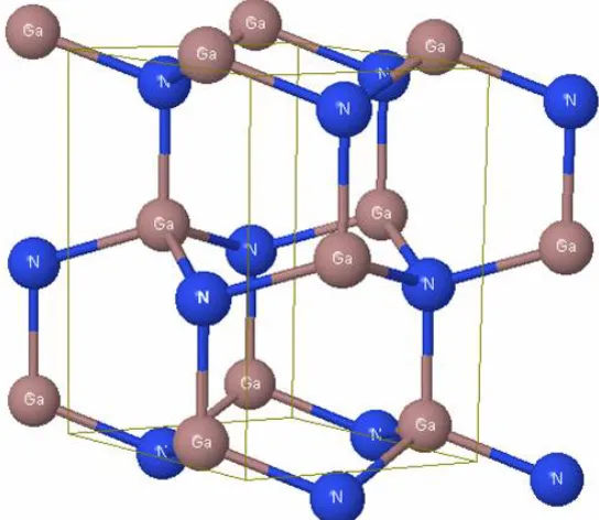
hexagonal symmetry. For reference other common semiconductor materials such as silicon (Si) and gallium arsenide (GaAs) have a diamond or zinc-blende structure. A representation of the GaN wurtzite crystal structure is presented in Figure 2.
Figure 2: GaN wurtzite crystal structure7.
III-nitrides do not have a center of symmetry and as such are polar crystals. Thus they possess piezoelectric properties the impact of which will be discussed in a later section. The large difference in electronegativity between group III elements and nitrogen yields strong bond strengths. This results in the wide band gap energies shown in Figure 1. Because the intrinsic carrier concentration is an exponential function of the band gap energy and temperature, wide band gap materials have lower leakage and dark currents.
⎟ ⎠ ⎞ ⎜ ⎝ ⎛ − ⎟ ⎟ ⎠ ⎞ ⎜ ⎜ ⎝ ⎛ = kT E T m m m x
ni e h
2 exp 10 9 . 4 2 3 4 3 2 0
15 (2-1)
of these properties and the ability to tune emission, GaN alloy devices are being commercialized for light-emitting diode and laser diode applications.
Table 1: Physical properties of III-nitrides8.
Property GaN AlN InN
Room temperature band gap (eV) 3.4 6.2 0.9
Bond strength (eV) 2.20 2.88 1.93
Thermal Conductivity (W/cm-K) 1.3 3.2 0.8 Lattice constant a (Å) 3.189 3.112 3.545 Lattice constant c (Å) 5.186 4.982 5.703
2.2 Gallium nitride growth
The synthesis of GaN was first described in 1932 by Johnson et al.9. However, the resulting material was polycrystalline and as such not useful for semiconductor devices. It was not until 1980-1990’s that two major breakthroughs led to resurgence in GaN research: development of a buffer layer technique to obtain smooth non-polycrystalline films and demonstration of p-type doping. This was followed in the mid 1990s by the development of the two-flow MOCVD process that yielded improved growth uniformity. Currently research in GaN has become a field of its own as the growth in commercial devices continues. A list of several key developments that laid the technological framework for the current commercial success of GaN are listed presented below.
• Epitaxial deposition of GaN using hydride VPE10 • Employment of nucleation buffer layers11 • Use of magnesium to achieve p-type GaN12 • Development of the two-flow MOCVD process13
epitaxial growth of GaN. Among them, metal-organic chemical vapor deposition (MOCVD), molecular beam epitaxy (MBE) and hydride vapor phase epitaxy (HVPE) are the most common14.
One of the major challenges faced in the growth of GaN is availability of suitable substrates. With the exception of silicon on sapphire no other
semiconductor has been commercialized exclusively using heteroepitaxial
materials15. This is because bulk GaN has proven difficult to grow, in part due to the low solubility of nitrogen in gallium and the high vapor pressure of nitrogen on GaN. Recently bulk GaN has been grown by HVPE, but cost and availability make it prohibitive for use in LED applications.
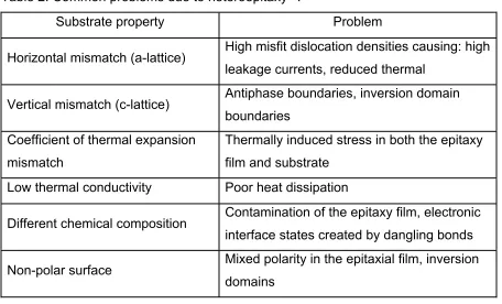
Table 2: Common problems due to heteroepitaxy15.
Substrate property Problem
Horizontal mismatch (a-lattice) High misfit dislocation densities causing: high leakage currents, reduced thermal
Vertical mismatch (c-lattice) Antiphase boundaries, inversion domain boundaries
Coefficient of thermal expansion mismatch
Thermally induced stress in both the epitaxy film and substrate
Low thermal conductivity Poor heat dissipation
Different chemical composition Contamination of the epitaxy film, electronic interface states created by dangling bonds Non-polar surface Mixed polarity in the epitaxial film, inversion
domains
A wide variety of substrates have been studied for GaN epitaxy a summary of which can be found in Liu and Edgar15. For GaN alloy LEDs the typical substrates are α-Al2O3 sapphire or 6H-SiC silicon carbide. Both substrates produce [0001]
orientated GaN. Of the two, sapphire is the most used substrate for III-nitride growth primarily because of cost. It has high thermal and chemical stability, and availability of large high quality wafers. Its drawbacks are large lattice and thermal conductivity mismatches to GaN and poor electrical conductivity. Silicon carbide has the closest match with GaN in regards to crystal symmetry, lattice and thermal conductivity. Electrically conductive substrates are available thereby allowing backside contacts simplifying the LED device structure compared to sapphire substrates. The primary drawback of silicon carbide is cost.
processes8. On the other hand, p-type doping of GaN has been problematic. This
obstacle was overcome by the addition of Mg as a dopant followed by post-growth irradiation by electron beam, which converted the Mg-compensated GaN into p-type GaN. Later, it was discovered that high-temperature annealing under nitrogen ambient works equally well to form p-GaN. However, Mg is a deep dopant and full ionization is not achieved. Nevertheless no other impurity has been as successful in yielding p-type GaN8.
In summary, the direct band gap energy range of GaN and its alloys make III-nitrides ideally suited for use in optoelectronic devices and are beginning to see acceptance in high power and high frequency applications. Cost and availability of a native substrate has required the use of heteroepitaxial materials for LED devices. The two most common substrates for GaN epitaxy are sapphire and silicon carbide. To achieve desired electrical properties GaN is typically doped with Si (n-type) and Mg (p-type).
2.3 Gallium nitride based LEDs
The achievement of p-type doping was critical in enabling the development of GaN based pn-junction LEDs. The first such device was reported in 1992 by
Akasaki et al.16 and emitted light in the ultraviolet range at a power of 42 μW. The LED was based on a pn-homojunction meaning that p- and n-sides were GaN just doped differently. In this configuration the recombination of injected carriers is governed by the diffusion length and occurs over a large region with a strongly changing minority carrier concentration. As radiative recombination is a function of free carrier concentration, it is critical that the region in which recombination occurs has a high carrier concentration6.
to the homojunction device17. In addition, by varying the indium mole relation,
InxGa1-xN and doping the active layer with Zn, blue to blue-green emission was
possible. However, poor crystal quality at indium mole fractions necessary for green band-edge emission limited application of double heterostructures devices.
p-GaN InGaN n-GaN
Conduction band
Valence band
p-GaN InGaN n-GaN
Conduction band
Valence band
Figure 3: Schematic of double heterostructure.
Drawbacks associated with double heterostructures were overcome by reducing the thickness of the active layer. First, if the active layer is sufficiently thin lattice-mismatch between the active and barrier layers is taken up by pseudomorphic strain and not by the formation of dislocations. Second, as the active layer width approaches the De-Broglie wavelength (≅ 3 nm for InGaN) quantum effects become apparent. When then the thickness is comparable to the De-Broglie wavelength the conduction and valence band energy states no longer behave as a continuum but become discreet and quantized (Figure 4). Under these conditions the active layer is now termed a quantum well (QW).
p-GaN InGaN n-GaN QW
Conduction band
Valence band
p-GaN InGaN n-GaN QW
Conduction band
Valence band
In 1994 Nakamura reported the first single quantum well (SQW) GaN based LED18. By varying the indium mole fraction in the In
xGa1-xN active layer from 0.2 to
0.7 the peak wavelength was varied from blue to yellow. Output powers ranged from 4 mW for blue, 1 mW for green and 0.5 mW for yellow LEDs. The drop in output power with increased wavelength reflects the decrease in crystal quality between the QW and barrier layers as both lattice mismatch and differences in thermal expansion coefficient increase with indium concentration. Lastly, the spectral width of QW based LEDs is significantly narrower than the first generation Zn doped heterostructure LEDs resulting in improved color purity. As such, the SQW and multiple quantum well (MQW) structures serve as the basis for today’s high-brightness GaN based LEDs.
2.4 Challenges
While the use of QW structures has improved several key LED performance metrics, several challenges still remain. GaN epilayers exhibit high dislocation
densities whose impact on optoelectronic properties is still controversial. There is no consensus on how defects influence luminescence. As such an improved
understanding of the defect behavior in GaN and impact on luminescence is
necessary in order to continue to advance the performance of LEDs. A summary of the major defects in GaN devices follows.
2.4.1 Substrate lattice mismatch
Cost and availability constraints of native substrates necessitated the
commercialization of GaN LEDs with heteroepitaxial materials. Typically grown on sapphire and silicon carbide, GaN epilayers contain large dislocation densities due primarily to lattice mismatch. With respect to GaN, Al2O3 has a 13% mismatch and
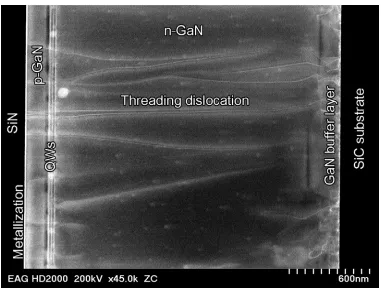
reduce the defect density. Never the less, in a typical GaN LED dislocation densities ranging from 108 – 1010 cm-2 are expected19. Figure 5 shows typical threading
dislocations observed in a GaN LEDs.
Figure 5: Threading dislocations in GaN.
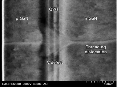
In addition, threading dislocations have been associated with a defect termed the ‘defect’ observed in the growth of InGaN MQW stacks. The structure of V-defects has been studied extensively and characterized as a hexagonal inverted pyramid that forms on the (0001) plane and the pyramid sidewalls are {10-11}20-25. Recently Liu et al.26 proposed a new method to determine the exact
The formation mechanism for V-defects is still being investigated, but is often reported to be induced by mixed threading dislocations, b=1/3<11-23>, during MQW growth. Liliental-Weber et al.27 proposed that formation of the defect is caused by
gettering. Impurities or dopant elements tend to congregate at dislocation sites and at high enough concentrations may locally inhibit crystal growth in the area of the dislocation, initiating V-defect formation. Cho et al.23 found that not all V-defects are connected with a threading dislocation. Instead stacking mismatch boundaries induced by stacking faults were proposed as an alternative origin for V-defects. Wu et al.22 proposed that V-defect formation is controlled kinetically by reduced GaN incorporation at lower growth temperatures. To suppress re-evaporation of indium, the growth temperature is lowered which reduces GaN surface diffusion, and thus the defect morphology is kinetically governed. As temperatures are increased for growth of p-GaN, surface diffusion rates are sufficiently high that the V-defects are back-filled/planarized by GaN.
While the structure and formation of V-defects has been investigated, little is know about their optoelectronic activity. It has been proposed that the V-defects contribute to carrier localization away from non-radiative sites. Hangleiter et al.28 and Netzel et al.29 reported that narrow QWs on the sidewalls of V-defects have higher band gap energy that effectively localizes carriers by providing an energy barrier around every defect. However, it has also been reported that V-defects have lower band gap energy and result in loss of light output22, 30. In short more studies
Figure 6: Typical V-defect.
Despite the large dislocation density, GaN based LEDs exhibit high optical efficiencies whereas for GaAs based LEDs dislocation densities > 106 cm-2 quench light emission2, 31, 32. As dislocations are thought to be non-radiative recombination sites, strong luminescence from GaN-based LEDs was surprising. This led to questions regarding the nature of dislocations and there interaction with other defects in the GaN material system.
2.4.2 Compositional variation
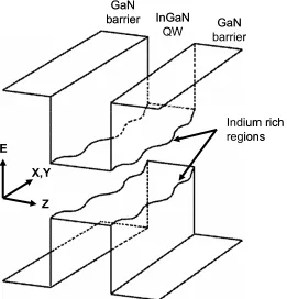
A spinodal is predicted in the InN-GaN phase diagram. Theoretical calculations by Ho and Stringfellow33 suggest that InGaN alloys are unstable over most of the
devices and the potential exists that the InGaN alloy will not be homogeneous. Thus the predicted spinodal has the potential to yield InN-rich and GaN-rich regions within InGaN QWs. The result of this phase separation would produce band gap variation as InN regions reduce the intended band gap as shown below in Figure 7.
InGaN QW GaN
barrier GaN
barrier
E
X,Y
Z
Indium rich regions InGaN
QW GaN
barrier GaN
barrier
E
X,Y
Z
Indium rich regions
Figure 7: Schematic of phase separation in InGaN QW (Adapted from Ponce34).
2.4.3 Quantum-confined stark effect
GaN alloy devices exhibit polarization effects due to the polarity difference between cation sites (Ga, In) and anion sites (N). Furthermore, wurtzite GaN is non-centrosymmetric which enables a polarization charge to manifest itself at hetero-interfaces. This is termed spontaneous polarization (Psp) as it is not induced by
strain, but by the difference in polarization constants across an interface. For our devices of interest we need to consider the polarization constants for GaN (-0.029 C/m2) and InN (-0.032 C/m2)8. Since the polarization constants are close, the effect of spontaneous polarization for InGaN/GaN structures is relatively small compared to the piezoelectric effect (Figure 8) which will now be discussed.
GaN barrier GaN barrier Å[0001] InGaN QW PPZ
PSP PSP PSP
GaN barrier GaN barrier Å[0001] InGaN QW PPZ
PSP PSP PSP
Figure 8: Schematic of spontaneous and piezoelectric polarization in wurtzite GaN.
Piezoelectric polarization (Ppz) results from lattice mismatch strain between
varies inversely with indium concentration; 3 nm for x = 0.1 to 1 nm for x = 0.2. Thus piezoelectric polarization is expected to increase as indium concentration is
increased to achieve longer wavelength emission.
At issue is an electric field (Epz) induced by piezoelectric polarization that can
affect the desired band structure and thus the optical and electrical properties of the device. Termed the quantum confined stark effect (QCSE) the presence of an electric field results in the band bending shown schematically in Figure 9.
GaN barrier GaN barrier InGaN QW CB VB EPZ Å[0001] GaN barrier GaN barrier InGaN QW CB VB Å[0001] b) a) GaN barrier GaN barrier InGaN QW CB VB EPZ Å[0001] GaN barrier GaN barrier InGaN QW CB VB Å[0001] b) a)
Figure 9: Schematic of band structure (a) with and (b) without band bending due to quantum confined stark effect.
The effect of band bending is two fold. First, the QCSE lowers the effective electron-hole pair recombination energy (dotted lines in Figure 9). This yields a red-shift in quantum well emission energy. The amount of red-shift is determined by the magnitude of the induced piezoelectric field which in turn is related to the lattice mismatch strain. Second, electrons and holes ‘pool’ in the energy minima resulting in a separation of their respective wavefunctions. The result is an increase in recombination time which potentially is a greater problem than the aforementioned red-shift. Increased recombination time allows carriers to find non-radiative
potential to negatively impact both emission efficiency and desired emission wave length.
2.4.4 Defect tolerant emission
GaN based LEDs exhibit strong emission despite a high density of threading dislocations, compositional fluctuations, and quantum confined stark effect2, 31, 39. Thus the question why is luminescence from GaN based LEDs relatively insensitive to defects. The answer to this is still open to debate and research continues.
At the heart of the question is the high dislocation density 108 – 1010 cm-2 associated with GaN devices. Because GaN LEDs have strong emission, initially it was thought that dislocations in GaN were not electrically active. That is to say dislocations do not act as carrier traps by forming mid-level states within the band gap. Attempts to correlate defects to luminescence have been made by numerous research groups 40-43. Results are still contradictory with some groups asserting dislocations are electrically active44 while others report the opposite45, 46. This is due to the difficulty of directly correlating defects to optical and electrical properties which will be discussed further in the next chapter. While the optoelectronic behavior of threading dislocations is still unclear, there is strong correlation between
non-radiative recombination sites and threading dislocation density39. If dislocations are non-radiative recombination sites, then some characteristic of the GaN alloy system is impeding charge carriers from reaching those sites.
The most common explanation for how charge carriers avoid nonradiative defects is compositional inhomogeneity within the QWs. In 1996 Chichibu et al.40
attributed the electroluminescence peak for an InGaN LED to recombination of EHPs localized at energy minima due to InN-rich regions less than 60 nm in size. Localization of the carriers in the indium enriched region helps keep them away from non-radiative recombination sites. Several groups attempted to investigate
the formation of In-rich regions49. Pooling due to the QCSE has been proposed as
the localization mechanism impeding carriers from reaching non-radiative sites50-52.
However, InGaN QWs grown on non-polar GaN which does not exhibit the QCSE, yielded recombination dynamics similar to those observed with polar GaN.
Recently, Chichibu et al. proposed that localization occurs on a much smaller scale and is due to atomic condensates of In-N spontaneously formed in statistically homogeneous InGaN alloys39. Observations of extremely short positron diffusion lengths (~ 4 nm) in indium alloys lead the authors to conclude the presence of a high density of sites capable of efficiently capturing positrons and thus, holes.
Identification of the sites came from two independent studies. Both Kent and Zunger53 and Wang54 using large-scale atomistic empirical pseudopotential
calculations predicted strong hole localization due to randomly formed condensates of In-N, which form deep acceptors. At this size scale direct observation of the atomic condensates will be difficult and has yet to be reported in literature.
2.4.5 Research motivation
While many different theories have been proposed, the origin of high
luminescence efficiency of GaN alloy LEDs still remains elusive. This research was undertaken to address questions related to the relatively defect tolerant optical and electrical properties of GaN based LEDs. The focus is on direct correlation of defects to optoelectronic behavior. This work also supports the advancement of optoelectronic analytical techniques using electron beam testing which is the topic of the next chapter. Lastly, it is fitting to conclude this chapter by describing the
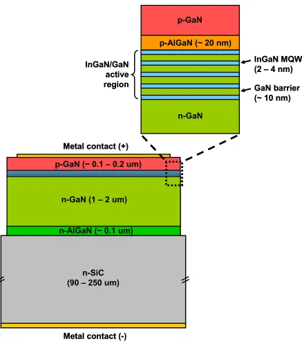
n-GaN (1 – 2 um)
n-AlGaN (~ 0.1 um)
n-SiC (90 – 250 um) Metal contact (+)
Metal contact (-) p-GaN (~ 0.1 – 0.2 um)
p-GaN
p-AlGaN (~ 20 nm)
n-GaN InGaN/GaN
active region
InGaN MQW (2 – 4 nm) GaN barrier (~ 10 nm)
n-GaN (1 – 2 um)
n-AlGaN (~ 0.1 um)
n-SiC (90 – 250 um) Metal contact (+)
Metal contact (-) p-GaN (~ 0.1 – 0.2 um)
p-GaN
p-AlGaN (~ 20 nm)
n-GaN InGaN/GaN
active region
InGaN MQW (2 – 4 nm) GaN barrier (~ 10 nm)
3. Analytical Techniques
3.1 Electron beam induced signals of interest
The interaction of an electron beam with a sample produces a rich set of signals of interest which are summarized in Figure 11. The electron beam-specimen interactions are a result of elastic and inelastic scattering processes that occur simultaneously within the sample55.
Cathodoluminescence (CL) Backscattered Electrons X-rays Secondary Electrons Incident Electron Beam Current Amplifier Electron beam induced current (EBIC) Transmitted
•Bright Field/High Angle Annular Dark Field
•Electron energy loss spectroscopy Sample Cathodoluminescence (CL) Backscattered Electrons X-rays Secondary Electrons Incident Electron Beam Current Amplifier Electron beam induced current (EBIC) Transmitted
•Bright Field/High Angle Annular Dark Field
•Electron energy loss spectroscopy
Sample
Figure 11: Electron beam generated signals of interest (Adapted from Williams and Carter56).
small angular changes to the electron trajectory with energy loss. The transfer of energy from incident electrons to the tightly bound inner-shell electrons and loosely bound outer-shell electrons of the atoms in the specimen gives rise to phonons (lattice vibrations), plasmons (electron oscillations), auger electrons, x-rays, photons, secondary electrons (SE), and electron-hole pair (EHP) generation55. During any given inelastic scattering event the incident electron can transfer an amount of energy ranging from less than 1 eV to the full energy carried by the electron. As inelastic scattering is an energy loss event it limits the distance traveled by the incident electrons within the sample.
The region in which the electrons interact with the sample, deposit energy and generate signals is called the interaction volume. The size of the interaction volume is a function of the mean atomic number, weight and density of the sample, the electron energy, spot size and incident angle55. Depending on these parameters the interaction volume can extend from a few nanometers to a few microns below the surface.
Understanding the size and shape of the interaction volume is crucial to understanding and interpretation of electron microscopy data. Estimates of the interaction volume are made by determining the distance traveled by incident
electrons within the sample (electron range). The most common approach is to use Monte Carlo modeling based of an established energy-loss law for electron beam interactions with a solid57. Monte Carlo simulations generate plots of the probable electron paths within a sample. By running several thousand simulations an estimate of interaction volume is obtained. Figure 12 shows a simulation from the Monte Carlo software Casino58, which illustrates the interaction volume resulting
Figure 12: Casino data of a 30 keV electron beam incident on bulk GaN.
From this result we can get an estimate of the depth ~ 2.6 μm and width ~ 4 μm of the interaction volume. As this is the region within which electrons interact with the sample the figure above underlines to importance of knowing where signals of interest are generated as that will impact resolution limits.
3.2 Electron beam induced current
In the absence of a separating force, EHPs will either recombine amongst themselves or due to localized concentration gradients diffuse to recombination sites. Under these conditions an EBIC signal is not produced. Alternatively, the presence of an electric field causes drift of nearby EHPs. The field applied either externally or internally will separate electrons and holes creating a current IEBIC
which can then be detected by an external circuit. Collection and imaging of a sample with the induced current is known as EBIC microscopy.
As an electric field is required, semiconductors devices that exhibit rectifying junctions are perfect candidates for EBIC analysis. Rectifying junctions have a ‘built-in’ electric field resulting from the depletion of free carriers in the space charge region. Beam injected EHPs within a diffusion length (L) of the space charge region will get separated with electrons swept to the n-side and holes to the p-side
generating IEBIC. A schematic of a typical cross-sectional EBIC experiment is shown
below in Figure 13 with the electron beam scanned parallel to the junction.
n-side
p-side
Current
Amplifier
E
0Scanning Electron Beam
Space charge layer
I
EBIC
n-side
p-side
Current
Amplifier
E
0Scanning Electron Beam
Space charge layer
I
EBIC
Figure 13: Schematic of cross-sectional EBIC experiment.
The magnitude of IEBIC depends on the number of EHPs generated and
generated within diffusion length of the space charge region feel the effect of the built-in electric field. As the field strength reaches a maximum at the pn-junction, the probability of EHP separation reaches a maximum as well. Therefore the EBIC signal is expected to peak at the pn-junction and then drop off. The signal can also be affected by the presence of defects which trap charge carriers and prevent them from contributing to IEBIC. Defects increase recombination rate, and reduce the
recombination lifetime, of minority carriers. As such, areas near a recombination-enhancing defect have a high contrast and appear dark in an EBIC micrograph.
For the evaluation of defects it is also useful to scan the electron beam
perpendicular to the pn-junction in what is called plan-view EBIC. This allows planar mapping of defects as recombination sites will appear dark due to lower IEBIC from
those regions. An example of a typical plan-view EBIC experiment is shown below in Figure 14.
Current Amplifier
I
EBIC
E
0Scanning Electron Beam
Space charge layer
n-side
p-side
Current AmplifierI
EBIC
E
0Scanning Electron Beam
Space charge layer
n-side
p-side
Figure 14: Schematic of plan-view EBIC experiment.
3.3 Cathodoluminescence
optoelectronic behavior of the sample. Other forms of luminescence exist and are classified according to their excitation method. Electroluminescence (EL) is the emission of photons due to an applied electrical field and is the operational mode for LEDs. Photoluminescence (PL) is due to photoexcitation excitation. As the most common way to perform CL experiments is with an electron microscope the remainder of this discussion will concentrate on cathodoluminescence.
CL microscopy can be broken into three broad categories; spectroscopy, panchromatic imaging and spectroscopic imaging. Spectroscopy is performed by investigating the spectral distribution of light. This yields information on the energies of different transitions in the sample. A number of transitions are possible that include but are not limited to; band-to-band, sub-band gap, excitonic and defect assisted. Panchromatic imaging spatially maps all the emitted wavelengths within the response of the detector. This enables the identification of high and low radiative recombination areas. As defects typically arrest radiative recombination, panchromatic imaging is used to target areas of interest for further investigation. Spectroscopic imaging combines spectral response with imaging to map emission from a particular wavelength band. This allows a particular emission to be mapped and spatially related to the sample structure.
In order to perform CL microscopy requires the electron microscope be specially equipped with some form of high efficiency light collection and detection apparatus. An example of a typical CL collection set-up is shown in Figure 15.
Mirror
Sample
Optics
CL dectector Fiber optic
(figure not to scale) Electron beam CL Photons Mirror Sample Optics CL dectector Fiber optic
(figure not to scale) Electron beam
CL Photons
Ideally the sample is positioned at the focal point of a large collection mirror. Emitted photons are collected and focused onto a fiber optic feed through to an ex-vacuo detector. The detector typically consists of a monochromator with a
photomultiplier or CCD array.
In addition CL set-ups often include cold-stages to suppress non-radiative processes which are typically thermally activated. This is important because the internal quantum efficiency η defined by Yacobi and Holt62 affects emission intensity.
⎥⎦ ⎤ ⎢⎣ ⎡− + = =
kT E R
R
A N
R
exp 1
1
η (3-1)
Where RR and RN are the radiative and non-radiative recombination rates
respectively, EA is activation energy, k is Boltzmann constant and T is temperature.
Equation (3-1) indicates that emission is stronger at low temperatures than higher temperatures.
3.4 Electron-hole pairs
The magnitude of IEBIC and CL intensity is a function of the number of EHPs
Band gap Electron Hole Conduction band Valence band Electron beam Electron beam a) b) Band gap Electron Hole Conduction band Valence band Electron beam Electron beam a) b)
Figure 16: Schematic of electron beam induced EHP generation in (a) band energy and (b) bond diagrams.
There are various methods to estimate the rate of EHP generation G. In general any method for determining G must account for recombination and
scattering losses. From Newbury63 the most common method for determining G at
SEM energies starts by calculating the number of EHPs created per second, G0.
b eh i qE n E
G0 = (1− ) (3-2)
Where E is incident electron beam energy, n is bulk backscattering coefficient, q is electron charge, Eeh is average energy required to produce an EHP and ib is incident
electron beam current. While E and ib are determined from the microscope set-up, n
and Eeh are obtained by other methods. Estimates for the bulk backscattering
coefficient can be obtained from Monte Carlo simulations. Determining Eeh is more
challenging as it is a reflection of the complete electron interaction process. To simplify it is common practice to assume Eeh = 3Ebandgap. As n accounts for scattered
electrons lost to EHP formation we now need to account for EHPs lost to recombination. This is done by multiplying G0 by the estimated minority carrier
be noted that this estimate for G is based on SEM energies. At higher accelerating voltages relativistic effects appear and estimates for G based on Newbury’s method are suspect. The question of EHP generation at high electron energies will be discussed in a later section on high-resolution electron beam testing.
Semiconductors are doped to achieve specific electrical properties and the generation of EHPs can affect the engineered carrier concentrations. This can potentially alter the electrical behavior of the sample and leads to a discussion on low/high-injection conditions. First, consider an n-doped semiconductor. At equilibrium the concentration of electrons, majority carriers, is much greater than holes, minority carriers. Under low-injection conditions EHP generation of minority carriers (holes in this case) is less than the initial number of majority carriers. Now recall that EHP formation generates an equal number of electron and holes. In order to maintain charge neutrality, the relatively small number of excess majority carriers will drift to follow the diffusive motion of these minority carriers. Consequently the motion of both majority and minority carriers can be characterized by one parameter, the minority diffusion coefficient. This greatly simplifies modeling of carrier behavior. Under high-injection conditions EHP generation of minority carriers exceeds the initial number of majority carriers. This complicates the diffusion model by requiring the use of coefficients for both majority and minority carries. In addition, the large number of minority carriers may saturate defect sites resulting in changes to the sample behavior.
3.5 High-resolution electron beam testing
features of the QWs within the active layer. On the other hand Figure 17 (c) shows that the combination of high energy electron beam and thin sample decrease the size of the interaction volume and nanometer spatial resolution is possible.
<100 nm
a) b) c)
4.0 um
30 keV
200 nm
Bulk GaN sample 5 keV
Bulk GaN sample
200 keV
Thin GaN sample
≤300 nm
≈nm
<100 nm
a) b) c)
4.0 um
30 keV
200 nm
Bulk GaN sample 5 keV
Bulk GaN sample
200 keV
Thin GaN sample
≤300 nm
≈nm
Figure 17: Effect of beam energy and sample thickness on interaction volume (figure not to scale).
Condenser Lens Scanning Coil Bulk Sample Thin Sample Image Formation Lens
Screen or Film
Electron Gun 200kV
1kV~30kV Monitor SE Detector TEM TEM SEM SEM Objective Lens Movable Aperture Condenser Lens Scanning Coil Bulk Sample Thin Sample Image Formation Lens
Screen or Film
Electron Gun 200kV
1kV~30kV Monitor SE Detector TEM TEM SEM SEM Objective Lens Movable Aperture
Figure 18: Comparison of SEM and TEM configurations.
In a STEM the electron beam is focused on and rastered across the sample. In addition to SE, BSE, x-rays, photons, and EHPs, electrons transmitted through the sample can be detected with a high-angle annular dark field (HAADF) detector or a bright field (BF) detector. The HAADF detector is an annular detector placed concentrically about the post-specimen optical axis. The HAADF detector detects transmitted electrons that have been scattered through high angles. The
acceptance angle of the HAADF detector is typically between 50mrad-200mrad, but can often be controlled with a projector lens. HAADF images are often called ‘Z-contrast’ images because the cross section for Rutherford elastic scattering is proportional to Z2. Consequently, high-Z regions of a specimen would scatter more
electrons and have a higher intensity than low-Z regions64, 65. The BF detector is an
axial detector that is usually placed after the HAADF detector and detects
Condenser Lens
Scannning Coils
Thin Sample
Z Contrast Detector (HAADF) Monitor
SE Detector
Bright Field Detector Objective Lens Movable Aperture
Electron Gun (200 kV) STEM
STEM
Condenser Lens
Scannning Coils
Thin Sample
Z Contrast Detector (HAADF) Monitor
SE Detector
Bright Field Detector Objective Lens Movable Aperture
Electron Gun (200 kV) STEM
STEM
Figure 19: Schematic of a STEM.
Intended for applications requiring highly localized nanoanalysis with energy dispersive x-ray spectroscopy (EDS) and electron energy loss spectroscopy (EELS), the first dedicated STEM was produced in 1963 by Vacuum Generators
STEM is capable of operation under several different modes (beam currents). An example of one such setting is ‘normal’ mode with a beam current of ~1 nA and a final spot size of ~ 0.5 nm.
Transmission electron microscopy and scanning transmission microscopy overcome the resolutions limits of conventional standard electron microscopies. These techniques are utilized to examine the internal structure of thin samples, which are electron transparent (Figure 20). For this application a ‘thin’ sample is one that is on the order of a few hundred nanometers thick. To simultaneously measure electro-optical properties with techniques such as EBIC or CL requires specialized TEM/STEM set-ups and sample prep. A discussion on instrument set-up for STEM-EBIC and –CL follows. A discussion on sample prep is reserved for chapter 4.
Scanning Electron Beam
Sample cross-section
n-GaN
p-GaN MQWs
25 nm
Scanning Electron Beam
Sample cross-section
n-GaN
p-GaN MQWs
25 nm
Figure 20: Schematic STEM based characterization.
3.6 STEM EBIC 3.5.1 Introduction
While EBIC identifies electrical activity of defects it is not effective in identifying the crystallographic nature of defects. On the other hand TEM/STEM techniques are capable of nanometer spatial resolution and the identification of defect structure. To fully characterize a defect, EBIC must be combined with either TEM or STEM techniques. The resulting STEM-EBIC technique is a powerful tool for the direct characterization of electrical transport properties to defects in
semiconductor materials66.
3.5.2 STEM-EBIC systems
The first TEM-EBIC system was demonstrated in 1977 by Sparrow and Valde on a Cambridge TEM equipped with a scanning attachment. Results correlated crystal defects with electrical properties in silicon transistors67. In 1978 Petroff et al. modified a TEM to perform simultaneous structural- EBIC analysis of dislocation cores and nonradiative recombination properties in GaAlAsP59. The first STEM-EBIC system was developed in 1980 by Fathy et al68. Interestingly, neither group
Figure 21: Isometric drawing of STEM-EBIC holder (From Perrreault and Ast69).
The unshielded signal wires passed to a BNC cable which transferred the signal from the sample to a Keithley 427, low-noise current amplifier. Functionality of the holder was demonstrated with the observation of electrically active defects in silicon Schottky diodes. In 2003 Bunker et al. developed a STEM-EBIC holder for the Hitachi HD-2000 series of microscopes70. Unlike the design by Perreault and Ast, the design by Bunker et al. electrically isolated the sample from the body of the holder. This was done to reduce potential noise from scattered electrons hitting the body of the holder. From the electrically isolated sample two Kapton insulated wires were connected to a subminiature A (SMA) connector that transferred the EBIC signal to a Keithley 614 electrometer.
3.5.3 Applications to GaN
electrical connections necessary for STEM-EBIC. To our knowledge the only
specific application was by Bunker et al. in 2003. In their paper they reported on an application of the STEM-EBIC technique for determining pn-junction location in InGaN SQW LEDs. Using simultaneous collection of Z-contrast and EBIC images they were able to position the pn-junction with nanometer resolution. Comparing the peak in the Z-contrast image to the peak in the EBIC image the pn-junction was located 19 ± 3 nm from the center of the InGaN QW (Figure 22).
Figure 22: EBIC and Z-contrast line scans showing relative location of pn-junction. (From Bunker et al.,70).
The results reported by Bunker et al. invite further investigations by STEM-EBIC of GaN based devices and in particular LEDs. Their investigation was limited to SQW devices, but most commercial LEDs now incorporate MQWs. In this