AES-GCM in Dynamically Reconfigurable Systems
Yohei Hori1, Akashi Satoh1, Hirofumi Sakane1, and Kenji Toda1 National Institute of Advanced Industrial Science and Technology (AIST)
1-1-1 Umezono, Tsukuba-shi, Ibaraki 305-8568, Japan
Abstract. A secure and dependable dynamic partial reconfiguration (DPR) sys-tem based on the AES-GCM cipher is developed, where the reconfigurable IP cores are protected by encrypting and authenticating their bitstreams with AES-GCM. In DPR systems, bitstream authentication is essential for avoiding fatal damage caused by inadvertent bitstreams. Although encryption-only systems can prevent bitstream cloning and reverse engineering, they cannot prevent erroneous or malicious bitstreams from being accepted as valid. If a bitstream error is de-tected after the system has already been partly configured, the system must be re-configured with an errorless bitstream or at worst rebooted since the DPR changes the hardware architecture itself and the system cannot recover itself to the initial state by asserting a reset signal. In this regard, our system can recover from con-figuration errors without rebooting. To the authors’ best knowledge, this is the first DPR system featuring both bitstream protection and error recovery mecha-nisms. Additionally, we clarify the relationship between the computation time and the bitstream block size, and derive the optimal internal memory size necessary to achieve the highest throughput. Furthermore, we implemented an AES-GCM-based DPR system targeting the Virtex-5 device on an off-the-shelf board, and demonstrated that all functions of bitstream decryption, verification, configura-tion, and error recovery work correctly. This paper clarifies the throughput, the hardware utilization, and the optimal memory configuration of said DPR system.
1
Introduction
Some recent Field-Programmable Gate Arrays (FPGAs) provide the ability ofdynamic partial reconfiguration (DPR), where a portion of the circuit is replaced with another module while the rest of the circuit remains fully operational. By using DPR, the func-tionality of the system is reactively altered by replacing hardware modules according to, for example, user requests, performance requirements, or environmental changes. To date, various applications of DPR have been reported: content distribution security [1], low-power crypto-modules [2], video processing [3], automotive systems [4], fault-tolerant systems [5] and software-defined radio [6] among others. It is expected that in the near future, it will be more popular for mobile terminals and consumer electron-ics to download hardware modules from the Internet in accordance with the intended use.
In DPR systems where intellectual property (IP) cores are downloaded from net-works, encrypting the hardware configuration data (=bitstream) is a requisite for pro-tecting the IP cores against illegal cloning and reverse engineering. Several FPGA fami-lies have embedded decryptors and can be configured using encrypted bitstreams. How-ever, such embedded decryptors are available only for the entire configuration and not
for DPR. In addition to bitstream encryption, bitstream authentication is significant for protecting DPR systems [7]. Encryption-only systems are not sufficiently secure as they cannot prevent erroneous or malicious bitstreams from being used for configuration. Since DPR changes the hardware architecture of the circuits, unauthorized bitstreams can cause fatal, unrecoverable damage to the system. In this regard, a mechanism of error recovery is essential for the practical use of DPR systems. If a bitstream error is detected after the bitstream has already been partly configured, the system must be reconfigured with an errorless bitstream. Note that the system cannot be recovered by asserting a reset signal since the hardware architecture itself has changed.
Based on the above considerations, we developed a DPR system which is capable of protecting bitstreams using AES-GCM (Advanced Encryption Standard [8]-Galois/Counter Mode [9,10]) and recovering from configuration errors. To the authors’ best knowledge, a DPR system featuring all mechanisms of bitstream encryption, bitstream verification and error recovery has not yet been developed, although several systems without recov-ery mechanism have been reported so far [11–13].
AES-GCM is one of the latest authenticated encryption (AE) ciphers which can guarantee both the confidentiality and the authenticity of message, and therefore AE could be effectively applied to DPR systems. Indeed, data encryption and authentication can be achieved with two separate algorithms, but if the area and speed performance of the two algorithms are not balanced, the overall performance is determined by the worse-performing algorithm. Therefore, AE is expected to enable more area-efficient and high-speed DPR implementations. Since other AE algorithms are not parallelizable or pipelinable, and thus not necessarily suitable for hardware implementation [14], the use of AES-GCM is currently the best solution for protecting bitstreams.
The configuration of a downloaded IP core starts after its bitstream is successfully verified. Bitstreams of large IP cores are split into several blocks, and verification is per-formed for each block. If the bitstream verification of a particular block fails after some other blocks have already been configured, the configuration process is abandoned, and reconfiguration starts with an initialization bitstream. In this configuration method, the size of the split bitstream significantly influences both the speed and the area perfor-mance. Since the decrypted bitstream must not flow out of the device and is thus stored to the internal memory, the size of the split bitstream determines the required memory resources. Although it is often thought that the speed performance can be improved by increasing the size of the available memory, our study revealed that the overall through-put can be maximized by using optimally sized internal memory.
This paper describes the architecture, memory configuration, implementation re-sults, and performance evaluation of an AES-GCM-based DPR system featuring an error recovery mechanism. The system is implemented targeting Virtex-5 on an off -the-shelf board, and we demonstrate that its mechanisms of bitstream encryption, verifica-tion and error recovery work successfully. The rest of this paper is organized as follows. Section 2 introduces past studies on DPR security. Section 3 explains the process of partial reconfiguration of a Xilinx FPGA. Section 4 briefly explains the cryptographic algorithms related to our implementation. Section 5 describes the architecture of our DPR system and explains the functions implemented in it. Section 6 determines the op-timal memory configuration of the DPR system and describes the experimental results, implementation results, and evaluation of the systems. Finally, Section 7 summarizes this paper and presents future work.
2
Related Work
Xilinx Virtex series devices support configuration through encrypted bitstreams by uti-lizing built-in bitstream decryptors. Virtex-II and Virtex-II Pro support the Triple Data Encryption Standard (Triple-DES) [15] with a 56-bit key, while Virtex-4 and Virtex-5 support AES with a 256-bit key. The key is stored to the dedicated volatile memory inside the FPGA. Therefore, the storage must always be supplied with power through an external battery. Unfortunately, the functionality of configuration through encrypted bitstreams is not available when using DPR, and if the device is configured using the built-in bitstream decryptor, the DPR function is disabled. Therefore, in DPR systems, partial bitstreams must be decrypted by utilizing user logic.
Bossuet et al. proposed a secure configuration method for DPR systems [11]. Their system allows the use of arbitrary cryptographic algorithms since the bitstream decryp-tor itself is implemented as a reconfigurable module. However, although their method uses bitstream encryption, it does not consider the authenticity of the bitstreams.
Zeineddini and Gaj developed a DPR system which uses separate encryption and au-thentication algorithms for bitstream protection [12], where AES was used for bitstream encryption and SHA-1 for authentication. AES and SHA-1 were implemented as C pro-grams and run on two types of embedded microprocessors: PowerPC and MicroBlaze. The total processing times needed for the authentication, decryption, and configuration of a 14-KB bitstream on PowerPC and MicroBlaze were approximately 400 ms and 2.3 sec, respectively. Such performances, however, would be insufficient for practical DPR systems.
Parelkar used AE to protect FPGA bitstreams [13], and implemented various AE algorithms: Offset CodeBook (OCB) [16], Counter with CBC-MAC (CCM) [17] and EAX [18] modes of operation with AES. In order to compare the performance of the AE method with separate encryption and authentication methods, SHA-1 and SHA-512 were also implemented using AES-ECB (Electronic CodeBook).
3
Partial Reconfiguration of FPGAs
This section briefly describes the architecture of Xilinx FPGAs and the features of par-tial reconfiguration with Xilinx devices. Detailed information about Xilinx FPGAs can be found in [19,20]. For more detailed information about Xilinx partial reconfiguration, see [21].
3.1 Xilinx FPGA
Xilinx FPGAs consist ofConfigurable Logic Blocks (CLBs), which compute various logic, and an interconnection area which connects the CLBs. CLBs are composed of several reconfigurable units calledslices, and slices in turn contain severallook-up ta-bles (LUTs), which are the smallest reconfigurable logic units. In Virtex-5, each CLB contains two slices, and each slice contains four 6-input LUTs. In Virtex-4 and earlier Virtex series devices, each CLB contains four slices, and each slice contains two 4-input LUTs. While the LUTs can be used as memory, Xilinx FPGAs also contain dedicated memory blocks referred to as BlockRAMs or BRAMs.
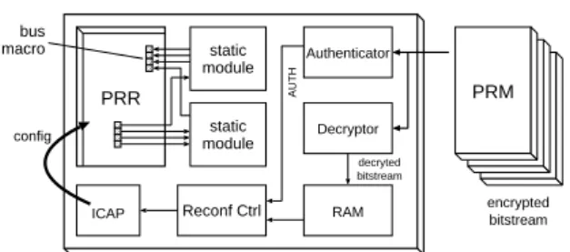
bus macro PRR static module static module ICAP Reconf Ctrl Decryptor RAM Authenticator PRM config encrypted bitstream decryted bitstream AUTH
Fig. 1.Structure of a partially reconfigurable circuit in a Xilinx FPGA.
Virtex-II Pro Virtex-5
Partially Reconfigurable Module (PRM) Frame Clock Region Boundary 20 CLBs
Fig. 2.Frame of Xilinx FPGAs.
3.2 Partial Reconfiguration Overview
In Xilinx FPGAs, modules which can be dynamically replaced are calledPartially Re-configurable Modules (PRMs), and the areas where PRMs are placed are called Par-tially Reconfigurable Regions (PRRs). PRMs are rectangular and can be of arbitrary size. Figure 1 shows an example structure of the partially reconfigurable design.
The smallest unit of a bitstream which can be accessed is called aframe. In Virtex-5 devices, a frame designates a 1312-bit piece of configuration information corresponding to the height of 20 CLBs. A bitstream of PRMs is a collection of frames. In Virtex-II Pro and earlier Virtex devices, the height of the frame is the same as the height of the device. Figure 2 illustrates the frames of Virtex-II Pro and Virtex-5.
3.3 Bus Macro
All signals between the PRMs and the fixed modules must pass throughbus macros
in order to lock the wiring. In Virtex-5 devices, the bus macros are 4-bit-wide pre-routed macros composed of four 6-input Lookup Tables (LUTs). The bus macros must be placed inside the PRMs. Furthermore, the bus macros of older device families are 8-bit-wide pre-routed macros composed of sixteen 4-input LUTs, which are placed on the PRM boundary.
3.4 Internal Configuration Access Port
Virtex-II and newer Virtex series devices supportself DPRthrough theInternal Con-figuration Access Port(ICAP). ICAPs practically work in the same manner as the Se-lectMAP configuration interface. Since user logic can access the configuration memory
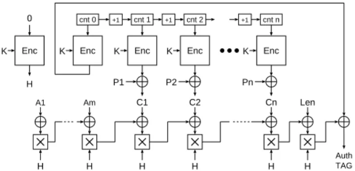
Enc P1 C1 K Enc C2 K Enc Cn K P2 Pn cnt 1 cnt 2 cnt n H H H Len H Enc K 0 H +1 +1 Enc K cnt 0 +1 Auth TAG H Am H A1
Fig. 3.Example operation of the Galois/Counter Mode (GCM).
through ICAPs, the partial reconfiguration of FPGAs can be controlled by internal user logic. In Virtex-5 devices, the data width of the ICAP can be set to 8, 16 or 32 bits.
4
Cryptographic Algorithm
4.1 Advanced Encryption Standard
AES is a symmetric key block cipher algorithm standardized by the U.S. National In-stitute of Standard and Technologies (NIST) [8]. AES replaces the previous Data En-cryption Standard (DES) [22], whose 56-bit key is currently considered too short and not sufficiently secure. The block length of AES is 128 bits, and the key length can be set to 128, 196, or 256 bits.
4.2 Galois/Counter Mode of Operation
The GCM [9] is one of the latest modes of operation standardized by NIST [10]. Fig-ure 3 shows an example of GCM operation mode.
In order to generate a message authentication code (MAC), which is also called a
security tag, GCM uses universal hashing based on product-sum operation in the finite fieldGF(2w). The product-sum operation inGF(2w) enables faster and more compact hardware implementation compared to integer computation. The encryption and the de-cryption scheme of GCM is based on the CTR mode of operation [23], which can be highly parallelized and pipelined. Therefore, GCM is suitable for hardware implemen-tation, entailing a wide variety of performance advantages such as compactness to high speed [24, 25]. Other AE algorithms are not necessarily suitable for hardware imple-mentation as they are impossible to parallelize or pipeline [14].
AES-GCM is one of the GCM applications which uses AES as the encryption core. Since AES is also based on the product-sum operation inGF(2w), either compact or high-speed hardware implementation is possible. Therefore, the use of AES-GCM can meet various performance requirements and is the best solution for protecting FPGA bitstreams in DPR systems.
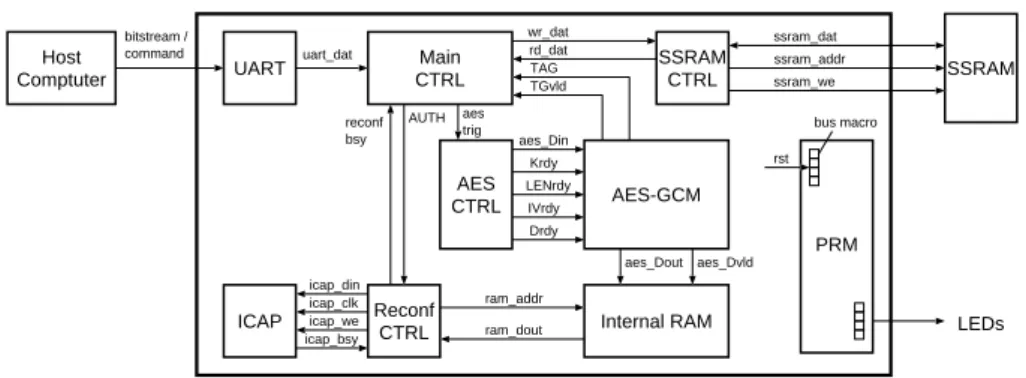
UART Main CTRL Reconf CTRL SSRAM CTRL Internal RAM ICAP SSRAM LEDs aes_Din Drdy Krdy IVrdy LENrdy uart_dat wr_dat rd_dat TGvld ssram_dat ssram_addr ssram_we bitstream / command Host Comptuter AES CTRL AES-GCM aes trig AUTH PRM aes_Dout aes_Dvld TAG ram_addr ram_dout icap_din icap_we icap_clk icap_bsy reconf bsy bus macro rst
Fig. 4.Overview of the system using AES-GCM.
5
AES-GCM-based DPR Systems
This section describes the architecture of our DPR system, which uses AES-GCM for bitstream encryption/decryption and verification and is capable of recovering from con-figuration errors. Figure 4 shows a block diagram of said system. The length of the AES key and the initial vector (IV) are set to 128 bits and 96 bits, respectively, and the AES key is embedded into the system.
5.1 Configuration Flow Overview
Encrypted bitstreams from PRMs are transferred from the host computer via RS232 and are stored to the external 36x256K-bit SSRAM. The configuration of the PRM starts when a configuration command is sent from the host computer. The downloaded bitstreams are decrypted by the AES-GCM module, and their authenticity is verified si-multaneously. Since the plain bitstreams must not leak out to the device, the decrypted bitstreams must be stored to the internal memory (Block RAM). Furthermore, since the size of the internal memory is relatively small, large bitstreams are split into several blocks, and decryption and verification is performed to each bitstream block. To distin-guish the divided bitstream block from the AES 128-bit data block, we define the former asBitstream Block(BSB). In the system, the memory size is set to 128x2kbits, and is at most 128x8192 (1 Mb) due to device resource limitations. After the integrity of the bitstream has been verified, the decrypted bitstream is read from the internal memory and transferred to the ICAP to configure the PRM.
Note that AES-GCM requires initial processing such as key scheduling and IV setup for each BSB. Therefore, the computation effort for the same bitstream increases with the number of BSBs. The smaller the internal memory is, the more compact the sys-tem will be; however, computation effort will increase. Conversely, if the memory size is large, computation effort will decrease, although the system will require more hard-ware resources. Furthermore, since additional data such as a security tag, IV, and data length, are attached to each BSB, the size of the downloaded data increases with the number of BSBs. The trade-offbetween internal memory size, downloaded data size and computation effort is clarified in Section 5.3 and Section 5.4.
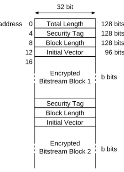
Total Length Security Tag Block Length Initial Vector Security Tag Block Length Initial Vector Encrypted Bitstream Block 1 Encrypted Bitstream Block 2 32 bit address 0 4 8 12 b bits b bits 128 bits 128 bits 128 bits 96 bits 16
Fig. 5.General structure of bitstreams stored to SSRAM.
The consideration is that simply dividing a bitstream into several BSBs will be vulnerable againstremovalorinsertionof a BSB. Though AES-GCM can detect tam-pering with the BSB, it does not care the number or order of the successive BSBs. For example, even if one of the successive BSBs is removed, AES-GCM cannot detect the disappearance of the BSB and thus the system would be incompletely configured. In addition, if a malicious BSB with its correct security tag is inserted to the series of the BSBs, AES-GCM will recognize the inserted BSB as legitimate and thus the malicious BSB will be configured in the device, causing system malfunction, data leakage and so on. Therefore, some protection scheme to prevent BSB removal and insertion is nec-essary for DPR systems. The protection scheme against these problems is discussed in section 5.7.
5.2 Data Structure
In order to decrypt a PRM bitstream with AES-GCM, information about the security tag, data length, and IV need to be appended to the head of the bitstream. Large bit-streams are divided into several BSBs, and each BSB contains such header information. In addition, the first BSB contains information about the total bitstream length. Figure 5 shows the structure of the downloaded bitstream together with the header information, which is loaded from SSRAM and set to the registers in the AES-GCM module when the PRM configuration begins.
5.3 Bitstream Decryption and Verification
In the AES-GCM module, the major component (the S-box) is implemented using com-posite field. The initial setup of AES-GCM takes 59 cycles, and the first BSB takes 19 additional cycles for setting up the total length of the entire bitstream. A 128-bit data
block is decrypted in 13 clock cycles, including SSRAM access time, and the decrypted data are stored to the internal memory. The last block of BSB requires 10 clock cycles in addition to the usual 13 for the purpose of calculating the security tag. The secu-rity tag is calculated usingGHAS Hfunction defined below, whereAis the additional authentication data,Cis the ciphertext andHis the hash subkey.
Xi= 0 i=0 (Xi−1⊕Ai)·H i=1, . . . ,m−1 (Xm−1⊕(A∗m||0128−v))·H i=m (Xi−1⊕Ci−m)·H i=m+1, . . . ,m+n−1 (Xm+n−1⊕(Cn∗||0128−u))·H i=m+n (Xm+n⊕(len(A)||len(C)))·H i=m+n+1 (1)
The final valueXm+n+1becomes the security tag. InGHAS Hfunction, the 128 x 128-bit
multiplication over Galois Field (GF) is achieved using 128 x 16-bit GF multiplier eight times for saving the hardware resources. Fig.6 shows the GF multiplier implemented in the AES-GCM module. The partial products of the 128 x 16-bit multiplier are summed up into the 128-bit registerZ. The calculation ofZfinishes in 8 clock cycles.
An example timing chart of the AES-GCM module including the initial setup is shown in Figure 7. Suppose that the size of the entire bitstream isS bits, and that it is split intonBSBs. Let the size of thekth BSB bebkbits, andb1,b2, . . . ,bn−1 be BSBs
of the same sizeb. Then, the entire sizeS is expressed as follows:
S = n X k=1 bk= n−1 X k=1 b+bn=(n−1)·b+bn. (2)
As Figure 7 illustrates, the required number of clock cyclesTaesfor the decryption and verification of the entire bitstream is
Taes =19+(n−1)· 59+13· b 128+10+2 ! + 59+13· bn 128+10+2 ! =19+13 (n−1)b+13bn 128 +71n =13S 128 +71n+19 (∵S =(n−1)b+bn). (3)
As the above equation indicates, the computation effort for AES-GCM increases with the number of BSBsn.
5.4 PRM Configuration
Unlike other DPR systems, our system does not use an embedded processor to control the partial reconfiguration. The input data and control signals from the ICAP are directly connected to and controlled by the user logic. Thus, our system is free from the delay of processor buses. In the system, the width of the ICAP data port is set to 32 bits. When the frequency of the input data to the ICAP is f [MHz], the throughput of the reconfiguration processPicapis
s127 s126 s 7 s 6 s 5 s 4 s 3 s2 s 1 s 0 h 15 h 14 h 13 h 0 a127 a126 a 7 a 6 a 5 a 4 a 3 a 2 a 1 a 0 Z 127 Z 126 Z 7 Z 6 Z 5 Z 4 Z 3 Z 2 Z 1 Z 0 16 16 Z X H a 128 h 128 A 128 0 Xi 128 128 s
128-bit x 16-bit multiplier
Fig. 6.The architecture of the Galois Field multiplier.
40 4 4 30 13 23 1 1 3 s/32
AES initial setup Decryption & Verification
PRM config 78 13*s/128 +10 1st bitstram block 21 4 4 30 13 2
AES initial setup
59 Krdy TGrdy LENrdy IVrdy Drdy TGvld AUTH Reconf Reconf_BSY 23 1 3 s/32 + 5 PRM config 2nd bitstram block (last block)
2 13*s/128 +10
(block size = s [bit])
Decryption & Verification
In Virtex-5, the maximum frequency of the ICAP is limited to 100 MHz, thus the ideal throughput of the reconfiguration process is 3,200 Mbps.
Figure 7 also shows the timing of the configuration of the PRM bitstream. When the size of the BSB isbbits, the configuration of the BSB finishes inb/32 cycles. The last BSB takes 5 additional cycles to flush the buffer in the device. Therefore, the required number of computation cycles for the PRM configurationTrecon fis
Trecon f =(n−1)· b 32+ bn 32+5 ! = S 32+5 (∵S =(n−1)b+bn). (5) 5.5 Error Recovery
In the system, the first several bytes of the SSRAM are reserved for theinitialization PRM, which is used for recovering the system from DPR errors. The use of the initial-ization PRM enables the system to return to the start-up state without rebooting the en-tire system. Thus, processes executed in other modules can retain their data even when DPR errors occur. The bitstream of the initialization PRM is encrypted and processed in the same way as that of other PRMs. If the bitstream size isS bits, the computation time for decryption, verification, and configuration is derived from equations (3) and (5).
When bitstream verification fails with AES-GCM, the current process is abandoned and configuration of the initialization PRM is started. Note that the unauthorized BSB is still in the internal memory and it will be overwritten by the initial PRM. Therefore, the unauthorized bitstream will be safely erased and will not be configured in the system. If the verification of the initialization PRM fails due to, for example, bitstream tampering or memory bus damage, the system discontinues the configuration process and prompts the user to reboot the system.
5.6 Overall Computation Time
The decryption, verification, and configuration of the BSBs is processed in a course-grained pipeline, as shown in Figure 7. The configuration of all BSBs except the last BSB overlaps with the decryption process. Therefore, the total computation time T, including bitstream encryption, verification, and configuration, is
T = 13 128S +71n+19 ! + bn 32 +5 ! = 13 128S +71n+ bn 32+24. (6)
If the bitstream encryption, verification and configuration cannot be processed in a pipeline, the total number of computation cyclesT0is
T0=Taes+Trecon f = 13 128S +71n+19 ! + S 32+5 = 17 128S +71n+24. (7)
Considering thatS ≥bn, the improvement of the computation time due to the use of a course-grained pipeline architecture is
T0−T = S −bn
32 (≥0). (8)
5.7 Countermeasure against BSB Removal and Insertion
As mentioned in section 5.1, dividing the bitstream into several BSBs is vulnerable against attacks of BSB removal and insertion. One scheme to protect such attacks is to use sequential numbers as the initial vector (IV) for calculating security tag. In this protection scheme, each BSB has Block Number (BN) that denotes the position of the BSB in the bitstream. The initial BN is unique to each PRM. The BN of the first BSB is used as IV and simultaneously stored to the internal register or memory. The stored BN is incremented and used as IV every time a BSB is loaded. If the loaded BSB has different BN from the stored value, the configuration is immediately terminated and the recovery process is started.
The computation time slightly increases when BN is used for the bitstream protec-tion, because reading BN from SSRAM takes several clock cycles. Suppose that the length of BN islBN. The clock cycles required to read BN aredlBN/32e, as the width of the SSRAM is 32 bits. In this case, the total computation time with pipeline processing (TBN) is TBN= 13 128S + 71+ & lBN 32 '! n+19 ! + bn 32+5 ! = 13 128S + 71+ & lBN 32 '! n+bn 32+24. (9)
The increased time due to the use of BN is
TBN−T = & lBN 32 ' n. (10)
The equation (10) indicates that the additional BN will have more effect on computation time as the number of the BSBsnincreases. As is given in Section 6.2, the size ofnis typically 4 to 16. Thus, the time increase caused by using BN is quite small compared to the total computation time.
This study is the first step toward developing a secure practical DPR system and its main purpose is to demonstrate the feasibility of the recovery mechanism of the AES-GCM-based DPR system, so the additional protection logic with BN is currently not implemented. Implementing the additional protection logic is left as future work.
6
Implementation
This section describes the implementation results of the abovementioned AES-GCM-based DPR system (hereinafter PR-AES-GCM). PR-AES-GCM is implemented tar-geting Virtex-5 (XC5VLX50T-FFG1136) on an ML505 board [26]. The systems are designed using Xilinx Early Access Partial Reconfiguration (EA PR) flow [27] and are implemented with ISE 9.1.02i PR10 and PlanAhead 9.2.7 [28].
103 104 105 106 220 218 216 214 212 210 28
Computation cycles (T) [cycle]
Bitstream block size (s) [bit] min pipeline, S = 220 pipeline, S = 219 pipeline, S = 218 pipeline, S = 217 pipeline, S = 216 non-pipeline, S = 220 non-pipeline, S = 219 non-pipeline, S = 218 non-pipeline, S = 217 non-pipeline, S = 216
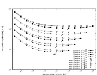
Fig. 8.Relationship between the BSB sizeband the total number of computation cyclesT and T0.
6.1 PRM Implementation
In order to test whether all mechanisms of bitstream encryption, verification, and er-ror recovery work properly, we implemented two simple function blocks, a 28-bit up-counter, and a 28-bit down-counter as PRMs. In addition, two bus macros were placed in the PRR for the input and output signals, respectively. The most significant 4 bits of the counter were the outputted from the PRM and connected to LEDs on the board. The PRR contained 80 slices, 640 LUTs, and 320 registers. The size of the bitstream for this area became about 12 KB (=96 K bits), which could change slightly depend-ing on the complexity of the implemented functions. The sizes of the up-counter and down-counter PRMs were 87,200 and 85,856 bits, respectively.
6.2 Internal Memory
In order to determine the required size of the internal memory, equation (6) should be transformed to express the relationship betweenT andb. For estimation purposes, we suppose that the size of the last BSBbnisbbits. In this case, equation (6) is rewritten as follows: T = 13 128S +71n+19 ! + bn 32 +5 ! = 13 128S + 71S b + b 32+24. (∵S =n·b) (11)
Figure 8 illustrates the variation of the total computation timeTin accordance with the BSB sizeb under the conditionsS = 216, 217, 218, 219 and 220. For comparison,
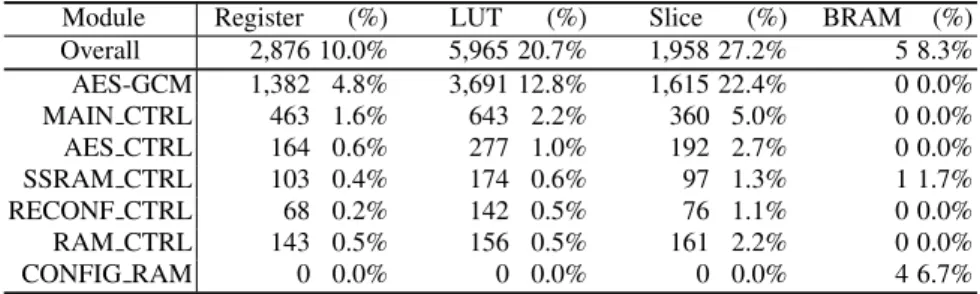
Table 1.Hardware utilization of the static module of PR-AES-GCM on Virtex-5 (XC5VLX50T).
Module Register (%) LUT (%) Slice (%) BRAM (%) Overall 2,876 10.0% 5,965 20.7% 1,958 27.2% 5 8.3% AES-GCM 1,382 4.8% 3,691 12.8% 1,615 22.4% 0 0.0% MAIN CTRL 463 1.6% 643 2.2% 360 5.0% 0 0.0% AES CTRL 164 0.6% 277 1.0% 192 2.7% 0 0.0% SSRAM CTRL 103 0.4% 174 0.6% 97 1.3% 1 1.7% RECONF CTRL 68 0.2% 142 0.5% 76 1.1% 0 0.0% RAM CTRL 143 0.5% 156 0.5% 161 2.2% 0 0.0% CONFIG RAM 0 0.0% 0 0.0% 0 0.0% 4 6.7%
equation (7) is transformed as follows, and its graph is also shown in Figure 8.
T0=Taes+Trecon f = 13 128S +71n+19 ! + S 32+5 = 17 128S + 71S b +24. (∵S =n·b) (12)
As Figure 8 clearly shows, the course-grained pipeline architecture is effective for shortening the overall processing time. The computation cycles in non-pipelined cir-cuits decrease monotonically, while those in pipelined circir-cuits have minimal values, as indicated by the arrows in Figure 8. When the entire sizeS is 216, 217, 218, 219 or 220,
the respective BSB sizesbwhich minimizeT are 214, 214, 215, 215 and 216.The most
time-efficient DPR systems were realized by setting the size of the internal memory to
bas derived here. Equation (11) is useful for balancing the computation time and circuit size under the required speed and area performance.
Incidentally, the system with the BN-based protection shows completely the same results as ones given above, that is, the respective optimal sizesbare 214, 214, 215, 215 and 216for the sameS values.
After deriving the relationship betweenT and b, we determined the most time-efficient memory configuration for the PRMs introduced in Section 6.1. The size S
should be set to a slightly larger value than the prepared PRMs in order to accommodate other PRMs with different sizes. Therefore,S is set to 217, which is the minimal 2w meeting the requirement 2w > 87200. As Figure 8 illustrates, the optimal BSB sizeb
under the conditionS =217is 214. Therefore, the internal memory configuration is set
to 128×128 (=214) bits.
6.3 Hardware Resource Utilization
Table 1 shows the hardware utilization of PR-AES-GCM implemented on a Virtex-5. The “Overall” item shows the total amount of hardware resources used by all mod-ules except PRM. Table 1 also describes the hardware utilization of each module as a standalone implementation.
The hardware architecture of Virtex-5 is vastly different from that of earlier devices such as Virtex-II Pro and Virtex-4. Each slice in Virtex-5 contains four 6-input LUTs,
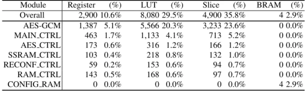
Table 2.Hardware utilization of the static module of PR-AES-GCM on Virtex-II Pro (XC2VP30).
Module Register (%) LUT (%) Slice (%) BRAM (%) Overall 2,900 10.6% 8,080 29.5% 4,900 35.8% 4 2.9% AES-GCM 1,387 5.1% 5,566 20.3% 3,233 23.6% 0 0.0% MAIN CTRL 463 1.7% 1,133 4.1% 713 5.2% 0 0.0% AES CTRL 173 0.6% 316 1.2% 166 1.2% 0 0.0% SSRAM CTRL 103 0.4% 218 0.8% 132 1.0% 0 0.0% RECONF CTRL 59 0.2% 153 0.6% 94 0.7% 0 0.0% RAM CTRL 143 0.5% 168 0.6% 97 0.7% 0 0.0% CONFIG RAM 0 0.0% 0 0.0% 0 0.0% 4 2.9%
Table 3.Comparison of the performances of different secure PR systems (14,112 bytes PRM).
System Device Slice Verification Decryption Configuration Overall Ratio PR-AES-GCM XC5VLX50T 4,900∗ 119.110µs 35.3µs 123.72µs 1 947.8 Mbps 3195 Mbps 913 Mbps PowerPC [12] XC2VP30 1,334∗∗ 139 ms 208 ms 56 ms 403 ms 3257 812 kbps 543 kbps 2016 kbps 280 kbps MicroBlaze [12] XC2VP30 1,706∗∗ 776 ms 1472 ms 32 ms 2280 ms 18429 145 kbps 77 kbps 3528 kbps 50 kbps AES-OCB [13] XC4VLX60 2,964 601 Mbps - -AES-CCM [13] XC4VLX60 2,799 255 Mbps - -AES-EAX [13] XC4VLX60 2,993 287 Mbps -
-∗The slice utilization of Virtex-II Pro is shown for the purpose of fair comparison. ∗∗Includes only the reconfiguration controllers.
whereas that of earlier devices contains two 4-input LUTs. Thus, the number of slices is smaller in the Virtex-5 implementation. In order to give a fair comparison with other studies, we also implemented the above system on a Virtex-II Pro (XC2VP30-FF896). The hardware utilization of PR-AES-GCM on Virtex-II Pro is given in Table 2.
Here we consider the hardware utilization of the additional protection logic using BN. The logic needs registers or memory to store BN and comparators to verify if the BSB has correct BN. In addition, an adder is required to increment the BN stored in the register. To estimate the required resources for the protection logic, we implemented it on Virtex-5 and Virtex-II Pro under the condition that the size of BN is 128 bits. As a result, the logic utilizes 129 registers, 173 LUTs and 45 slices on Virtex-5, and 129 registers, 194 LUTs and 99 slices on Virtex-II Pro. These utilizations are all less than 1% of the entire resources. Therefore, the additional circuit will have little effect on the resource utilization of the whole system.
6.4 DPR Experiments
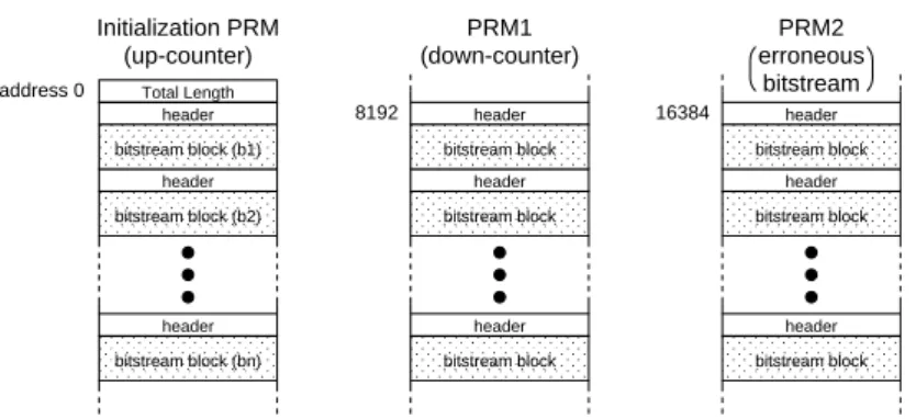
In order to experimentally demonstrate that all functions of bitstream encryption, verifi-cation, and configuration as well as the error recovery mechanism operate correctly, we configured the PRMs on the developed DPR system. Figure 9 shows the structure of the
Total Length header header header address 0 8192 16384 bitstream block (b1) bitstream block (b2) bitstream block (bn) Initialization PRM (up-counter) PRM1 (down-counter) PRM2 erroneous bitstream header header header bitstream block bitstream block bitstream block header header header bitstream block bitstream block bitstream block
Fig. 9.Bitstream structure in SSRAM in the DPR experiment.
bitstreams in the DPR experiment. The PRM with the up-counter (hereinafter PRM0) is placed at address 0 as the initialization bitstream, and the PRM with the down-counter (hereinafter PRM1) is placed at address 8192. Configuration with an erroneous bit-stream was emulated by inverting the first byte of the bitbit-stream of PRM1 and using the bitstream thus obtained for PRM2.
The experimental procedure is outlined below.
1. The system is booted. Note that the most significant 4 bits of the counter in the PRM0 are connected to LEDs on the board.
2. The configuration command is sent from the host computer with the SSRAM ad-dress “8192” to configure PRM1.
3. The bitstream at address 8192 is loaded from SSRAM, decrypted, verified, and configured.
4. The configuration command is sent from the host computer with the SSRAM ad-dress “16384” to configure PRM2.
5. The bitstream at address 16384 is loaded from SSRAM, decrypted, verified, and configured.
When the system was booted, the LEDs indicated that the up-counter was imple-mented in PRM0, and after PRM1 was configured, the LEDs indicated that the down-counter was implemented in PRM1. This result shows that the decryption and verifica-tion with AES-GCM worked correctly and that DPR was performed successfully.
After PRM2 was configured, the LEDs indicated that the up-counter was imple-mented in PRM0. Note that PRM2 is an erroneous bitstream generated based on the output of PRM1, which is equipped with the down-counter. This result shows that the configuration of PRM2 failed and the system was reconfigured with PRM0, which is equipped with the up-counter. Therefore, the error recovery mechanism was demon-strated to operate correctly.
6.5 Performance Evaluation
The clock frequency of PR-AES-GCM is 100 MHz. In order to enable comparison with [12], the computation time required to configure a 14,112-byte (112,896-bit) PRM
is described in Table 3. Decryption, verification, and configuration with PR-AES-GCM can be implemented in a pipeline, and the respective computation time is derived from equation (6).
In PowerPC and MicroBlaze systems, authentication, decryption, and reconfigura-tion are performed sequentially, and therefore the overall processing time is simply the sum of the processing times of each step. Table 3 also gives the throughput of other AE algorithms as reported in [13].
6.6 Analysis of the Results
The results of the experiment in Section 6.4 indicate that all functions of bitstream de-cryption, verification, configuration, and error recovery work properly. Thus, the system described above is the first operational DPR system featuring both bitstream protection and error recovery mechanisms.
As shown in Table 3, PR-AES-GCM achieved the highest overall throughput of over 900 Mbps with only about 1/3 slice utilization. Note that PR-AES-GCM includes error recovery logic, an SSRAM controller, etc. Additionally, the AES-GCM module achieved a throughput of about 950 Mbps, which is faster than those of other AE meth-ods of OCB, CCM, and EAX. It is remarkable that such high throughput is achieved with such small size of the internal memory as determined by equation (11). The per-formance of the system is often thought to improve as the memory size increases. How-ever, in course-grained DPR architectures, equation (11) reveals that optimally sized internal memory can maximize the throughput of the entire system. The device can ac-commodate at most 128×213bits of memory, while our system uses only 128×27bits. Therefore, sufficient memory resources are available for various user logic.
Furthermore, PowerPC and MicroBlaze DPR systems require an overall computa-tion time between several hundred milliseconds and several seconds, which is unac-ceptable for practical DPR systems. Therefore, authentication, decryption, and recon-figuration should be processed using dedicated hardware in order to realize practical DPR systems. Compared to software AE systems, our approach attained extremely high performance, where PR-AES-GCM achieved a 3257 times higher throughput than the PowerPC system and an 18429 times higher throughput than the MicroBlaze system.
7
Conclusions
We developed a secure and dependable dynamic partial reconfiguration (DPR) system featuring AES-GCM authentication and error recovery mechanisms. Furthermore, it was experimentally demonstrated that the functions of bitstream decryption, verifica-tion, configuraverifica-tion, and error recovery operate correctly. To the authors’ best knowl-edge, this is the first operational DPR system featuring both bitstream protection and error recovery mechanisms.
Through the implementation of the above system on a Virtex-5 (XC5VLX50T), AES-GCM achieved a throughput of about 950 Mbps, and the entire system achieved a throughput of more than 910 Mbps, which is sufficient for practical DPR use, and utilized only 1/3 of the slices. This performance is higher than that of other modes of operation such as OCB, CCM, and EAX.
Remarkably, it was found that using optimally sized internal memory entails the highest throughput in the DPR system. Although it is often thought that the performance of the system improves as the memory increases, our study revealed that optimizing the size of the internal memory depending on the size of the entire bitstream provides the shortest processing times. Thus, our system was able to achieve the highest throughput with the least amount of memory resources.
The future work of this study is to implement further security mechanisms to prevent attacks such as the bitstream block removal and insertion. This paper showed that the protection scheme using block numbers as the initial vector would be implemented with hardly sacrificing the computation time and hardware resources. Another future work is to develop various application systems, such as content distribution and multi-algorithm cryptoprocessors, based on the DPR system described above.
References
1. Hori, Y., Yokoyama, H., Sakane, H., Toda, K.: A secure content delivery system based on a partially reconfigurable FPGA. IEICE Trans. Inf.&Syst.E91-D(5) (May 2008) 1398–1407 2. Hori, Y., Sakane, H., Toda, K.: A study of the effectiveness of dynamic partial reconfiguration
for size and power reduction. In: IEICE Tech. Rep. RECONF2007-56. (January 2008) 31–36 (in Japanese).
3. Claus, C., Zeppenfeld, J., Muller, F., Stechele, W.: Using partial-run-time reconfigurable hardware to accelerate video processing in driver assistance system. In: DATE’07. (2007) 498–503
4. Becker, J., Hubner, M., Hettich, G., Constapel, R., Eisenmann, J., Luka, J.: Dynamic and partial FPGA exploitation. Proc. IEEE95(2) (2007) 438–452
5. Emmert, J., Stroud, C., Skaggs, B., Abramovici, M.: Dynamic fault tolerance in FPGAs via partial reconfiguration. In: FCCM 2000. (2000) 165–174
6. Delahaye, J.P., Gogniat, G., Roland, C., Bomel, P.: Software radio and dynamic reconfigu-ration on a DSP/FPGA platform. J. Frequenz58(5-6) (2004) 152–159
7. Drimer, S.: Authentication of FPGA bitstreams: Why and how. In: ARC’07. Volume LNCS 4419. (2007) 73–84
8. National Institute of Standards and Technology: Announcing the advanced encryption stan-dard (AES). FIPS PUB 197 (November 2001)
9. McGrew, D.A., Viega, J.: The Galois/counter mode of operation (GCM) (May 2005) http://
csrc.nist.gov/groups/ST/toolkit/BCM/modes development.html.
10. Dworkin, M.: Recommendation for Block Cipher Modes of Operation: Galois/Counter Mode (GCM) and GMAC. National Institute of Standards and Technology. SP 800-38D edn. (November 2007)
11. Bossuet, L., Gogniat, G.: Dynamically configurable security for SRAM FPGA bitstreams. Int. J. Embedded Systems2(1/2) (2006) 73–85
12. Zeineddini, A.S., Gaj, K.: Secure partial reconfiguration of FPGAs. In: ICFPT’05. (2005) 155–162
13. Parelkar, M.M.: Authenticated encryption in hardware. Master’s thesis, George Mason University (2005)
14. McGrew, D.A., Viega, J.: The security and performance of the Galois/counter mode (GCM) of operation. In: INDOCRYPT 2004. (2004) 343–355
15. National Institute of Standards and Technology: Recommendation for the triple data encryp-tion algorithm (TDEA) block cipher (May 2004)
16. Rogaway, P., Bellare, M., John, B.: OCB: A block-cipher mode of operation for efficient authenticated encryption. ACM Trans. Information and System Security6(3) (August 2003) 365–403
17. Whiting, D., Housley, R., Ferguson, N.: Counter with CBC-MAC (CCM). RFC3610 (September 2003)
18. Bellare, M., Rogaway, P., Wagner, D.: A conventional authenticated-encryption mode. http://www-08.nist.gov/groups/ST/toolkit/BCM/documents/proposedmodes/eax/ eax-spec.pdf (2003)
19. Xilinx, Inc.: Virtex-5 User Guide. (2007) 20. Xilinx, I.: Virtex-4 User Guide. (2007)
21. Lysaght, P., Blodget, B., Mason, J., Young, J., Bridgford, B.: Enhanced architectures, design methodologies and CAD tools for dynamic reconfiguration of Xilinx FPGAs. In: FPL’06. (2006) 12–17
22. U.S. Department of Commerce/National Institute of Standards and Technology: Data En-cryption Standard (DES). FIPS PUB 46-3 edn. (1999)
23. Dworkin, M.: Recommendation for Block Cipher Modes of Operation. National Institute of Standards and Technology. SP 800-38A edn. (December 2001)
24. Satoh, A.: High-speed parallel hardware architecture for Galois counter mode. In: ISCAS’07. (2007) 1863–1866
25. Satoh, A., Sugawara, T., Aoki, T.: High-speed pipelined hardware architecture for Galois counter mode. In: ISC’07. (2007) 118–129
26. Xilinx, Inc.: ML505/ML506 Evaluation Platform. UG347(v2.4) edn. (October 2007) 27. Xilinx, Inc.: Early Access Partial Reconfiguration User Guide For ISE 8.1.01i. (2006) 28. Jackson, B.: Partial Reconfiguration Design with PlanAhead 9.2. Xilinx, Inc. (August 2007)