APPLICATION NOTE
Introduction
The LCD monitors and TVs are growing very fast, so to support this kind of applications, a dedicated ref-erence design has been developed, taking into account all the requirements that are needed.
The proposed reference design can supply an LCD monitor or an LCD-TV as well, up to 22" panels, to-gether with multimedia functions like audio. The SMPS accepts a full range input voltage and delivers 2 output voltages, a 5V dedicated to the scaler and µP, and a 12V dedicated to the backlight and audio. The required standby power consumption is 0.8W at 230Vac, in order to satisfy the worldwide power saving rules. The circuit is also fully protected against faults like output short circuit or over voltage. The market cost pressure has requested a design approach with particular attention to the solution cost. The board technology used is the standard thru-hole, but it can be changed very easily in SMT because most of com-ponents are available also in this technology. The circuit has been tested deeply in all the most salient aspects with positive results and it has been integrated with a 22" LCD-TV application without showing any problem.
Main characteristics
INPUT VOLTAGE: 90 ÷ 265 Vrms - 45-66 Hz
OUTPUT VOLTAGES: 5.1V±2% - @2A Dedicated to panel and digital circuitry for scaling 12V±10% - @4A Dedicated to backlight lamp inverters, audio and SCART STANDBY Input power less than 0.8W @230Vac, delivering 30mA on 5.1V
FAULT PROTECTIONS: Short circuit on each output with auto-restart at short removal, Open loop Safety&EMC: Safety: Acc. to EN60950, creepage and clearance minimum distance 6.4mm
EMC: According to EN50022 Class-B PCB TYPE & SIZE: Cu Single Side 70 µm, CEM-1, 180 x 89 mm
by Claudio Spini
60W WIDE-RANGE POWER SUPPLY
FOR LCD MONITOR OR TV, USING THE L5991
This document describes a reference design for a 60W Switch Mode Power Supply dedicated to LCD TV sets or monitors. The board accepts full range input voltage (90 to 265Vrms) and delivers 5V and 12V. It has good efficiency and very good standby performance, able to meet the most stringent standby rules.
The converter topology of this SMPS is the standard fly back, working in discontinuous and continuous current mode. The operating frequency of the circuit (~50 kHz) has been chosen in order to obtain a com-promise between the transformer size and the input filter complexity. Hence, the input EMI filter is a simple Pi-filter, 1-cell only, for differential and common mode noise, using a 4-sectors coil filter. A NTC limits the inrush current at plug-in. The transformer is a slot type, manufactured by PULSE-ELDOR designed ac-cording to the EN60950. Ferrite size is ETD34, the reflected voltage is ~95V providing enough room for the leakage inductance voltage spike with still margin for reliability.
The reflected voltage, the switching frequency and the primary inductance have been chosen to allow the continuous current operation of the transformer at full load, all over the input voltage range. This helps to decrease the output capacitor size thanks to the better ratio between the rms and peak current. The net-work D10, C14, R5 clamps the peak of the leakage inductance voltage spike ensuring reliable operation of the PowerMOS, while C21, D11 and R19 limit the dv/dt of the drain voltage.
The PowerMOS is a low cost STP5NK80ZFP, offering a good trade-off between the V(BR)DSS, the RDS(on) and the equivalent COSS, housed in standard 220 or 220FP packages. In this design, the TO-220FP (TO-220 insulated) has been used, mounted on a heat sink and fixed by a spring. Core of this de-sign is the current mode primary controller, the L5991 integrating all the required blocks to manage the control and protection of an SMPS. It is available in either DIP-16 (L5991) or in SO-16 (L5991D) packages. The switching frequency is programmable by means of a an RC network (R11, R12, C15): during normal operation R11 and R12 are connected in parallel by an internal switch (pin 16); when a light load is de-tected by the controller this internal switch is opened and the resulting frequency becomes lower, pro-grammed only from C15 and R11.
If the load is further decreased the network D4, D5, R23 provides an additional frequency reduction, pro-portional to the load, allowing very low power consumption from the mains. Pins 15 and 3 are set in order to allow the full duty-cycle operation and so the use of most of the energy stored in the bulk capacitor dur-ing hold-up operations. Because of the current mode control and the possibility for the duty cycle to exceed 50%, a slope compensation circuitry has been added.
A latched, over voltage protection has been implemented by using the pin 14 and a simple resistor net-work: in case of loop failure the circuit senses the Vcc and, when the voltage at that pin exceeds the in-ternal threshold, the controller stops the operation until its Vcc drops below the UVLO voltage. The start-up is done using a non-dissipative charge pump circuit to save power during standby.
The output rectifiers have been chosen in accordance with the maximum reverse voltage and their power dissipation. The 5V rectifier is Schottky barrier type STPS5L40, a 5A-40V axial rectifier that thanks to the low-forward voltage drop is housed in a DO-201 package.
The 12V rectifier is an STPS8H100, an high voltage Schottky rectifier offering a good trade-off between the forward voltage drop and the maximum operating junction temperature. It is available from STM in 5 different package versions. For this design, the ISOWATT220AC (similar to a standard insulated TO-220) has been used, mounted on a heat sink and fixed by a spring.
On both outputs, an LC filter has been added in order to filter out the high frequency ripple without increas-ing the output capacitors size or quality. The output voltage regulation is performed by the secondary feed-back monitoring the 5.1V output. The feedfeed-back network is the typical one that uses a TL431 driving an optocoupler, in this case an SFH617A-2, to ensure the required insulation between primary and second-ary. The opto-transistor drives directly the COMP pin of the L5991. Here following some waveforms during the normal operation at full load:
Figure 2. Drain voltage & current @115 VAC
-60Hz - full load
Figure 3. Drain voltage & current @230 VAC
-50Hz - full load
The pictures here above show the drain voltage and current at the nominal input mains voltage during normal operation at full load. As visible, the circuit works in CCM both at nominal high and low mains.
The figure 4 shows the measurement of the drain peak voltage at full load and maximum input mains voltage. The measured voltage of 672V, ensures a reliable operation of the MOSFET with a good margin against the maximum BVDSS. Even the maximum rectifiers PIV have been measured
dur-ing the worst operatdur-ing condition and they are in-dicated on the right of figure 5. The margin, with respect to the maximum voltage withstood by each diode, ensures safe operating conditions for these devices.
Figure 4. Drain voltage & current @265 VAC
-50Hz - full load
Figure 5. Maximum rectifiers PIV @Vin = 265 VAC - 50 Hz and full load
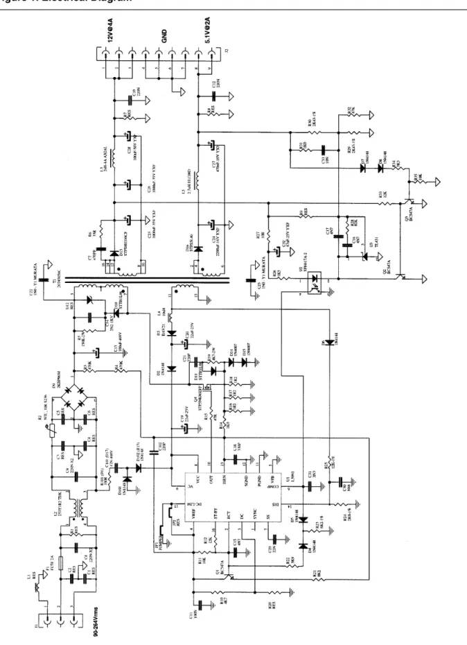
Here following the most salient controller IC sig-nals are shown. In both pictures it is possible to distinguish clean waveforms free of hard spikes or noise that could affect the controller correct oper-ation. CH1: VQ4 - Drain CH2: VPIN8 (Vcc) CH4: VR16 (Drain Current) CH1: VQ4 - Drain CH2: VPIN8 (Vcc) CH4: VR16 (Drain Current) CH1: VQ4 - Drain CH2: VPIN8 (Vcc) CH4: VR16 (Drain Current)
CH3: +5V RECTIFIER: Anode voltage CH4: +12V RECTIFIER: Anode voltage
Figure 6. Drain voltage & current @115 VAC
-60Hz - full load
Figure 7. Drain voltage & current @230 VAC
-50Hz - full load CH2: VPIN10 (Out) CH3: VPIN6 (Comp) CH4: VPIN2 (RCT) CH2: VPIN10 (Out) CH3: VPIN6 (Comp) CH4: VPIN2 (RCT) Cross regulation
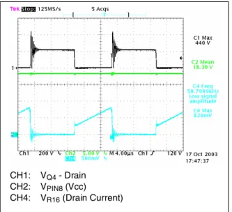
In the following tables it has been reported the output voltage cross regulation measurements with static loads. The overall efficiency of the converter is also calculated at the nominal input voltages.
To check the application circuit it has been tested keeping constant the current on the 5V and varying the 12V load. As visible in both tables, the voltages are within their tolerance at any load condition and the circuit efficiency is good
. 5V ± 2% 12V ± 10% TOLERANCE 115 Vac Vout [V] @Iout [A] Vout [V] @Iout [A] PoutTOT [W] Pin [W] Efficiency Vaux [V] fs [KHz] 5.106 2 12.11 4 OK 58.65 71.7 81.8% 18.3 51 5.107 2 12.23 3 OK 46.90 56.6 82.9% 17.4 51 5.108 2 12.40 2 OK 35.02 42.1 83.2% 16.7 51 5.110 2 12.72 1 OK 22.94 27.7 82.8% 16.5 51 5.110 2 13.11 0.5 OK 16.78 20.7 81.0% 16.6 51 5.108 1 11.85 4 OK 52.51 63.9 82.2% 17.5 51 5.108 1 12.00 3 OK 41.11 49.4 83.2% 16.7 51 5.110 1 12.15 2 OK 29.41 35.0 84.0% 16.2 51 5.112 1 12.39 1 OK 17.50 21.0 83.3% 15.9 51 5.112 1 12.66 0.5 OK 11.44 14.0 81.7% 15.9 51
Standby operation
Like in the previous section, the output voltages and the efficiency have been checked, and the input pow-er has been measured. It is clearly visible that with the required standby load (5V@30mA, 12V@0mA)
the input power consumption is well below 800mW at both the input voltage ranges. Besides, the cir-cuit has been characterised at both the nominal input voltage values for different output load and the effi-ciency is high in all conditions. In the fig. 8, it is shown the output voltage variation as a function of the 5V current.
During the standby operation the circuit works at reduced frequency, according to load and input voltage therefore, thanks to this function, the switching losses are minimized. This allows reaching very low stand-by consumption because in a power switch the switching and the capacitive losses are directly proportion-al to the working frequency.
5V ± 2% 12V ± 10% TOLERANCE 230 Vac Vout [V] @Iout [A] Vout [V] @Iout [A] PoutTOT [W] Pin [W] Efficiency Vaux [V] fs [KHz] 5.106 2 12.09 4 OK 58.57 69.3 84.5% 17.7 51 5.107 2 12.23 3 OK 46.90 55.3 84.8% 17.3 51 5.109 2 12.40 2 OK 35.02 41.2 85.0% 16.9 51 5.110 2 12.74 1 OK 22.96 27.6 83.2% 16.6 51 5.110 2 13.12 0.5 OK 16.78 20.8 80.7% 16.6 51 5.108 1 11.85 4 OK 52.51 63.9 82.2% 17.5 51 5.108 1 12.00 3 OK 41.11 49.4 83.2% 16.7 51 5.110 1 12.15 2 OK 29.41 35.0 84.0% 16.2 51 5.112 1 12.39 1 OK 17.50 21.0 83.3% 15.9 51 5.112 1 12.66 0.5 OK 11.44 14.0 81.7% 15.9 51 5V 115 Vac
Vout [V] @Iout [mA] PoutTOT [W] Pin [W] Efficiency
5.11 20 0.102 0.433 23.6% 5.11 30 0.153 0.515 29.8% 5.11 40 0.204 0.593 34.5% 5.11 50 0.256 0.667 38.3% 5.11 60 0.307 0.745 41.1% 5.11 80 0.409 0.881 46.4% 5.11 100 0.511 1.021 50.1% 5V 230Vac 5.11 20 0.102 0.493 20.7% 5.11 30 0.153 0.582 26.3% 5.11 40 0.204 0.672 30.4% 5.11 50 0.256 0.755 33.8% 5.11 60 0.307 0.842 36.4% 5.11 80 0.409 1.008 40.6% 5.11 100 0.511 1.168 43.8%
Figure 8. INPUT POWER @LOW LOAD
Here following, in figures 9 ad 10 some waveforms during standby are shown:
Figure 9. Standby @115 VAC - 60Hz 5V @50mA
load
Figure 10. Standby @230 VAC - 50Hz 5V @
50mA load
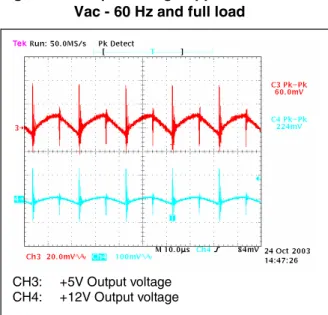
Output voltage ripple @full load
Figure 11. Output voltage ripple @Vin = 115 Vac - 60 Hz and full load
In figure 11 the output voltage ripples at switching frequency are measured. As shown, the ripple and the spikes are very low thanks to the addition-al LC filters added on both output and avoiding the use of bigger or expensive output capacitors. The residual line frequency modulation is very low at any input voltage.
Dynamic Load Tests
Figure 12 shows the output voltage regulation for a dynamic load variation of the 5V output. As shown in the picture the voltage variation and the response time are very good showing a good loop behaviour. In fact, the 5V voltage variation is less than 20mV (0,4%), and the spikes during the load transition, due to the filter inductor on the output, are only 75mV beyond the steady state (1,5%). The measured recovery time is few tens of micro-seconds. The variations induced on the 12V out-put have been also checked without showing any abnormal variation. Besides, the circuit response has been verified at minimum, nominal and maxi-mum input voltage, showing no significant change.
0.000 0.200 0.400 0.600 0.800 1.000 1.200 20 30 40 50 60 80 100 Iout +5V [mA] P in @ S ta nd -b y Pin @115Vac Pin@220Vac CH1: VQ4 - Drain CH2: VPIN8 (Vcc) CH4: VPIN6 (Comp) CH1: VQ4 - Drain CH2: VPIN8 (Vcc) CH4: VPIN6 (Comp) CH3: +5V Output voltage CH4: +12V Output voltage
Figure 12. +5V Dynamic load 1.5 ÷ 2A, 70Hz +12V: FULL LOAD - @115 VAC - 60Hz
In Figure 13 it is reported the response of the out-put voltages for a load variation of the 12V outout-put as detailed on top of the picture. The measure-ment has been done varying the 12V load from 50% to 100% load: the voltage variation is around 340mV and the 5V output is almost unaffected. Therefore, the conclusion is that there is no abnor-mal behaviour of the SMPS generated by a load change, allowing a good confidence for the inte-gration of the SMPS in the equipment.
Figure 13. +12V Dynamic load 2 ÷ 4A, 70Hz +5V: FULL LOAD - @115 VAC - 60Hz
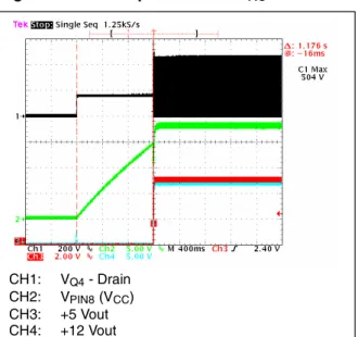
Start-Up Behaviour @full load and Wake-up time
In figure14 the wake-up time is measured at the lower nominal input mains and the controller start-up sequence is shown. The Vcc capacitor is charged by the charge pump circuit and when its voltage reaches the start-up threshold the device
starts to operate and the output voltages begin to rise up to the nominal value, where the control loop provides for the regulation. The wake-up time at 115Vac is 1.2 s, which is a quite typical time for this kind of Power Supplies. Besides, on the pic-ture it is clearly visible that no any overshoot, un-dershoot, dip or lost of control happens during the power supply start-up phase.
Figure 14. Wake-up time @115 VAC - 60Hz
Figure 15. Start-Up Behaviours @full load - @90 VAC - 60Hz
In the above picture the rising slopes at full load of the output voltages at minimum input mains volt-age are captured and the rise time is measured. As shown in the pictures, the rising time is mono-tonic and it is almost constant overall the input mains range. No any overshoot or abnormal be-haviour is present overall the input main range.
CH3: +5 Vout CH4: +12 Vout CH3: +5 Vout CH4: +12 Vout CH1: VQ4 - Drain CH2: VPIN8 (VCC) CH3: +5 Vout CH4: +12 Vout CH3: +5 Vout CH4: +12 Vout
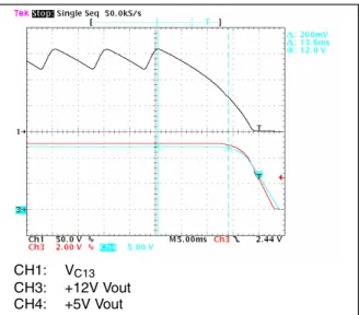
Turn-Off and Hold-up time
In figure 16 the most salient waveforms at turn-off are shown. Even at turn off the transition is clean, without abnormal behaviour like restarting at-tempts or loss of control by the loop. The Hold-up time, in evidence between the vertical lines, is 13.6 ms at 115Vac-50Hz, full load and becomes around 67ms at 230Vac.
Figure 16. Hold-up @115 VAC -50Hz - full load
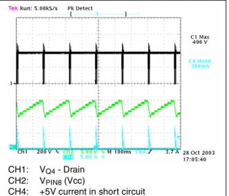
Short-Circuit Tests at Full Load
The short circuit tests have been done under sev-eral conditions, all over the input mains range. To avoid any catastrophic failure of the circuit due to overstress, a deep check of component stress has been done. The main circuit parameters that have been checked are the Mosfet drain voltage and the mean value of the output current. The drain volt-age is an important parameter to be monitored during short circuits because an excessive in-crease due to the transformer leakage inductance and the overcurrent flowing in the primary can cause the MOSFET BVDSS to be exceeded. In the proposed circuit, thanks to the low leakage induc-tance of the transformer and to the start-up com-ponent correct dimensioning, in case any output is shorted, the MOSFET drain voltage is below its BVDSS and the mean value of the output current is low too, thus preventing component overheating because of the excessive power dissipation. In this case the reliability against long term-shorts is not affected even at 264Vrms. The auto-restart at short removal has been also checked and it is cor-rect in all conditions.
Figure 17. Short circuit on 5V @90 VAC - 60Hz -
full load
Figure 18. Short circuit on 5V @265 VAC - 50Hz
- full load
As clearly indicated by the waveforms in figure 17 and 18, the circuit works in hiccup mode, keeping the mean value of the current at levels compatible with the component rating. As visible the circuit working time is constant because it depends only on the auxiliary capacitor value, while the dead time is inversely proportional to the input mains voltage. In the following figures 19 and 20 the waveforms relevant to the 12V output in short cir-cuit at both the nominal input mains voltage are re-ported: as visible, the circuit protects itself and the load. CH1: VC13 CH3: +12V Vout CH4: +5V Vout CH1: VQ4 - Drain CH2: VPIN8 (Vcc)
CH4: +5V short circuit current
CH1: VQ4 - Drain CH2: VPIN8 (Vcc)
Figure 19. Short circuit on 12V @90 VAC - 60Hz
- full load
Figure 20. Short circuit on 12V @265 VAC - 50Hz
- full load
Short Circuit Protection @ Low Load
After the full load tests, some checks on the short circuit protection with reduced loads have been done, as reported here following. The tests have been done even at minimum and maximum input voltage with the same results, as the previous tests.
@Half Load
The waveforms of figure 21 are relevant to a short circuit test simulating a fault during normal
opera-tions of the equipment, with a consumption halved with respect to the maximum output power levels (I+12V = 2A, I+5V = 1A).
– At Vin = 90Vac: shorting each output the over current protection works correctly, providing for the hiccup mode.
– At Vin = 265Vac: the circuit behaves correctly.
Figure 21. Short circuit on 5V @265 VAC - 50Hz
- half load
@Reduced Load
This condition simulates a fault during an operat-ing transition of the equipment, with the backlight off and a reduced consumption of the other output (I+12V = 0A, I+5V = 0.5A).
– At Vin = 90Vac: shorting each output the over current protection works correctly, providing for the hiccup working mode.
– At Vin = 265Vac: the behaviour of the circuit is correct like at 90Vac.
–
@Standby
This condition simulates a fault during the standby operation of the equipment, with the backlight and the scaler off, and the µP working with a reduced consumption (I+12V = 0A, I+5V = 33mA).
– At Vin = 90Vac: shorting each output the over-current protection works correctly, providing for the hiccup working mode.
– At Vin = 265Vac: the behaviour of the circuit is correct like at 115Vac.
CH1: VQ4 - Drain CH2: VPIN8 (Vcc)
CH4: +12V short circuit current
CH1: VQ4 - Drain CH2: VPIN8 (Vcc)
CH4: +12V short circuit current
CH1: VQ4 - Drain CH2: VPIN8 (Vcc)
Figure 22. Short circuit on 5V @265 VAC - 50Hz
- standby load
Figure 23. Short circuit on 12V @265 VAC -
50Hz - standby load
The main circuit parameter measurements have been done also during the test at reduced load or standby. In detail, during standby short it is possi-ble to check the perfect functionality of the protec-tion. This load condition in fact, is critical because all the power available from the converter can be delivered to one output only, because the others are lightly loaded or unloaded, and this can bring to the destruction of the rectifier of the shorted out-put. Besides, during standby operation, the trans-former coupling and the leakage inductance may be capable of supplying the controller charging the VDD capacitor by the spikes generated at Mosfet
turn-off, preventing the hiccup mode. To avoid this, the circuit around Q2 and Q3 has been add-ed, providing the hiccup mode anyway. As visible in the pictures, the SMPS is always protected even in this very critical load condition.
Over Voltage Protection
The open-loop operation is a very dangerous event that could happen in case of a feedback cir-cuitry failure. In this case, the SMPS output voltag-es can increase up to dangerous valuvoltag-es, depending on the load by each output and the transformer coupling between the windings. Thus, if the circuit is not properly protected, the rectifiers and the output capacitors can be overstressed and be destroyed or even worse, to catch light. To avoid this, the safety rules ask that the SMPS have a protection against the mentioned safety risks. In the proposed circuit, in case of a control loop fail-ure, a L5991 internal comparator stops the control-ler operation when the voltage at pin 14 (DIS) reaches 2.5V and remains latched until the Vcc voltage decreases below the UVLO threshold. So, a very safe protection with the L5991 is realized just by means of few passive components. The circuit has been tested opening the loop, the output voltages have been measured giving the following results overall the mains input voltage range:
As shown in the table, in both conditions the mea-sured voltages are not critical for the circuitry.
Conducted Noise Measurements (Pre-Compli-ance Test)
The following pictures are the peak conducted noise measurements at full load and nominal mains voltages. The limits shown on the diagrams are those specified by the EN55022 CLASS-B, which is the most widely used for Information Technology Equipment intended for domestic use, in the bandwidth 150KHz 30MHz. The filter config-uration used is the 2-wires one, without the ground connection at mains plug, suitable for domestic equipment like LCD-TVs. As visible on the dia-grams, there is a good margin between the peak measures with respect to the AVG limits (lower ones), and this assures that the QP and Average measures will be within their respective limits.
CH1: VQ4 - Drain CH2: VPIN8 (Vcc)
CH4: +5V current in short circuit
CH1: VQ4 - Drain CH2: VPIN8 (Vcc)
CH4: +5V current in short circuit
230Vac – 50Hz @FULL LOAD 230Vac – 50Hz @STANDBY 5V @ 2A 12V @ 4A 5V @ 0.03A 12V @0A V5V: 5.7V V12V: 13.5V V5V: 6.24V V12V: 15.8V
Figure 24. EN55022 Class-B Peak Measure @115 VAC - 60Hz - FULL LOAD
Figure 25. EN55022 Class-B Peak Measure 230 VAC - 50Hz - FULL LOAD
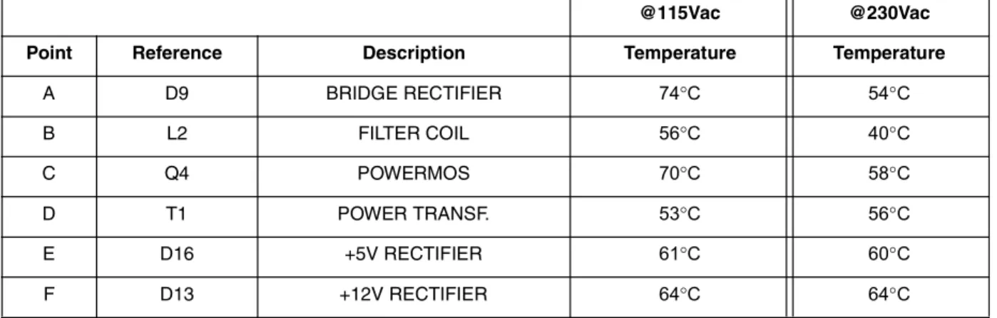
Thermal measures
In order to check the reliability of the design a thermal mapping by means of an IR camera has been done. In the table here below the temperature of some salient components is reported at 115Vac and 230Vac input voltage, at ambient temperature (24°C).
As visible in the above table there are not component working at a temperature level that can be consid-ered critical for their reliability.
@115Vac @230Vac
Point Reference Description Temperature Temperature
A D9 BRIDGE RECTIFIER 74°C 54°C B L2 FILTER COIL 56°C 40°C C Q4 POWERMOS 70°C 58°C D T1 POWER TRANSF. 53°C 56°C E D16 +5V RECTIFIER 61°C 60°C F D13 +12V RECTIFIER 64°C 64°C
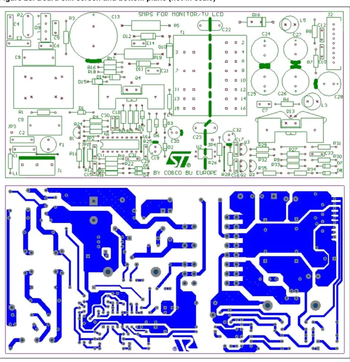
Board lay-out
Figure 26. Board silk-screen and bottom plane (not in scale)
■ Original size: 89x180mm
■ Copper thickness: 70µm
■ Material: CEM-1
Conclusions
An SMPS for LCD monitors or LCD-TV sets has been completely designed, assembled and tested using the L5991. All the different aspects (Component Electrical Stress, Functions, Protections, Conducted EMI, Thermal Stress) have been checked, giving positive results. The design meets also cost and low-complexity requirements, key factors in the Consumer Electronic market.
References
[1] "L5991 Data Sheet"
[2] "AN1537: A simple trick enhances L5991's standby function"
ANNEX1: Transformer spec
Transformer General Description
APPLICATION TYPE: Consumer, Home Appliance
TRANSFORMER TYPE: Open, Varnished only
WINDING TYPE Slot
COIL FORMER: Vertical type, 7+7 pins
MAX. TEMP. RISE: 45°C
MAX. OPERATING AMB. TEMP. : 60°C
MAINS INSULATION: ACC. WITH EN60065 - EN60950
Electrical Characteristics
CORE TYPE/GRADE: ETD34 - 3C90 or equivalent
PRIMARY INDUCTANCE: 825 µH ±10% @1KHz - 0.25V
LEAKAGE INDUCTANCE: 15 µH MAX @ 10KHz - 0.25V [1]
PEAK PRIMARY CURRENT: 2 Apk
[1]: Measured between pins 3-7 with all secondary shorted
PROVIDED BY PULSE-ELDOR P/N: 2074.5056C
Figure 27. Electrical Diagram
3 7 PRIM. 11 13 AUX 12 10 2- 6-+5V PRIMARY SECONDARY PINS: DC OUTPUT VOLTAGE: RMS CURRENT: NUMBER OF TURNS: 7-3 PRIMARY 0.84 ARMS 53 2/4-6/8 5V 2.6 ARMS 3 12-10 12V 5.3 ARMS 7 11-13 15V (AUX) 0.05 ARMS 9
ANNEX2: Part List
Designator Part Type/
Part Value Description Supplier
C1 RES NOT MOUNTED
C10 220N - 50V CERCAP AVX
C101 (D17) 47N-400V POLIESTER FILM CAP MKT R66 - ARCOTRONICS
C102 220P - 50V CERCAP AVX
C11 100N - 50V CERCAP AVX
C12 220N - 50V CERCAP AVX
C13 100uF-400V ALUMINIUM ELCAP LP4 SERIES - ELNA
C14 2N2-1KV HR HV CERCAP DEHR33A222K - MURATA
C15 4N7 - 50V CERCAP AVX
C16 4N7 - 50V CERCAP AVX
C17 4N7 - 50V CERCAP AVX
C18 330P - 50V CERCAP AVX
C19 22uF-25V ALUMINIUM ELCAP RUBYCON
C2 RES NOT MOUNTED
C20 22uF-25V ALUMINIUM ELCAP RUBYCON
C21 220PF-2KV HR HV CERCAP DEHR33A221K - MURATA
C22 1N0 - Y1 Y1 SAFETY CAP. DE1E3KX102M - MURATA
C23 1N0 - Y1 Y1 SAFETY CAP. DE1E3KX102M - MURATA
C24 2200uF-16V YXF ALUMINIUM ELCAP RUBYCON
C25 1000uF-35V YXF ALUMINIUM ELCAP RUBYCON
C26 1000uF-35V YXF ALUMINIUM ELCAP RUBYCON
C27 470uF-10V YXF ALUMINIUM ELCAP RUBYCON
C28 100uF-50V YXF ALUMINIUM ELCAP RUBYCON
C29 22N - 50V CERCAP AVX
C3 RES NOT MOUNTED
C30 N68 - 50V CERCAP AVX
C31 3N3 - 50V CERCAP AVX
C32 47uF-25V YXF ALUMINIUM ELCAP RUBYCON
C33 10N - 50V CERCAP AVX
C4 RES NOT MOUNTED
C5 RES NOT MOUNTED
C6 RES NOT MOUNTED
C7 470PF - 50V CERCAP AVX
C8 220N-X2 X2 FILM CAPACITOR R46-KI 3220 00 L2M - ARCOTRONICS
C9 220N-X2 X2 FILM CAPACITOR R46-KI 3220 00 L2M - ARCOTRONICS
D10 STTH1L06 FAST REC. RECTIFIER STMicroelectronics
D101 1N4148 GEN. PURPOSE DIODE WISHAY
D102 (R13) 1N4148 GEN. PURPOSE DIODE WISHAY
D11 STTH1L06 FAST REC. RECTIFIER STMicroelectronics
D12 RES NOT MOUNTED
D13 STPS8H100CF POWER SCHOTTKY RECT. STMicroelectronics
Designator Part Type/
Part Value Description Supplier
D15 1N4007 RECTIFIER DIODE WISHAY
D16 STPS5L40 POWER SCHOTTKY RECT. STMicroelectronics
D2 1N4148 GEN. PURPOSE DIODE WISHAY
D3 BAV21 GEN. PURPOSE DIODE WISHAY
D4 1N4148 GEN. PURPOSE DIODE WISHAY
D5 1N4148 GEN. PURPOSE DIODE WISHAY
D6 BAV21 GEN. PURPOSE DIODE WISHAY
D7 1N4148 GEN. PURPOSE DIODE WISHAY
D8 1N4148 GEN. PURPOSE DIODE WISHAY
D9 2KBP06M BRIDGE RECTIFIER WISHAY
F1 FUSE T2A FUSE 2 AMP. TIME DELAY WICKMANN
J1 INPUT CONNECTOR, 2/3 POLES, 7.5MM MOLEX
J2 OUTPUT CONNECTOR, 9 POLES, 2.54MM MOLEX
JP1 JUMPER WIRE JUMPER
JP2 RES NOT MOUNTED
L1 RES NOT MOUNTED
L2 253Y1R2 25mH-1.2A - CM FILTER INDUCTOR TDK
L3 2uH-4A 2uH-4A AXIAL FILTER INDUCTOR B82111 SERIES - EPCOS
L4 10uH RF AXIAL CHOKE B78108-S1103-K - EPCOS
L5 2.7uH DRUM COIL 2.7uH-4A ELC08D SERIES - PANASONIC
Q1 BC547A SMALL SIGNAL NPN BJT STMicroelectronics
Q2 BC547A SMALL SIGNAL NPN BJT STMicroelectronics
Q3 BC547A SMALL SIGNAL NPN BJT STMicroelectronics
Q4 STP5NK80ZFP POWER MOSFET STMicroelectronics
R1 RES NOT MOUNTED
R10 4K7 - 1/4W - 5% STANDARD FILM RESISTOR BEYSCHLAG
R101 (D1) 100R - 1/4W - 5% STANDARD FILM RESISTOR BEYSCHLAG
R11 10K - 1/4W - 5% STANDARD FILM RESISTOR BEYSCHLAG
R12 12K - 1/4W - 5% STANDARD FILM RESISTOR BEYSCHLAG
R14 1K0 - 1/4W - 5% STANDARD FILM RESISTOR BEYSCHLAG
R15 47R - 1/4W - 5% STANDARD FILM RESISTOR BEYSCHLAG
R16 1R2 - 1/4W - 5% STANDARD FILM RESISTOR BEYSCHLAG
R17 1R2 - 1/4W - 5% STANDARD FILM RESISTOR BEYSCHLAG
R18 1R2 - 1/4W - 5% STANDARD FILM RESISTOR BEYSCHLAG
R19 4K7 - 2W - 5% POWER RESISTOR 2W BEYSCHLAG
R2 NTC_10R S236 NTC THERMISTOR EPCOS
R20 RES NOT MOUNTED
R21 8K2 - 1/4W - 5% STANDARD FILM RESISTOR BEYSCHLAG
R22 3K9 - 1/4W - 5% STANDARD FILM RESISTOR BEYSCHLAG
R23 6K2 - 1/4W - 1% METAL FILM RESISTOR BEYSCHLAG
R24 2K0 - 1/4W - 1% METAL FILM RESISTOR BEYSCHLAG
R25 12K - 1/4W - 1% METAL FILM RESISTOR BEYSCHLAG
R26 1K5 - 1/4W - 5% STANDARD FILM RESISTOR BEYSCHLAG
Information furnished is believed to be accurate and reliable. However, STMicroelectronics assumes no responsibility for the consequences of use of such information nor for any infringement of patents or other rights of third parties which may result from its use. No license is granted by implication or otherwise under any patent or patent rights of STMicroelectronics. Specifications mentioned in this publication are subject to change without notice. This publication supersedes and replaces all information previously supplied. STMicroelectronics products are not authorized for use as critical components in life support devices or systems without express written approval of STMicroelectronics.
The ST logo is a registered trademark of STMicroelectronics. All other names are the property of their respective owners
© 2004 STMicroelectronics - All rights reserved STMicroelectronics GROUP OF COMPANIES
Australia - Belgium - Brazil - Canada - China - Czech Republic - Finland - France - Germany - Hong Kong - India - Israel - Italy - Japan - Malaysia - Malta - Morocco - Singapore - Spain - Sweden - Switzerland - United Kingdom - United States
www.st.com
Designator Part Type/
Part Value Description Supplier
R27 10R - 1/4W - 5% STANDARD FILM RESISTOR BEYSCHLAG
R28 82K - 1/4W - 5% STANDARD FILM RESISTOR BEYSCHLAG
R29 2K43 - 1/4W - 1% METAL FILM RESISTOR BEYSCHLAG
R3 470K - 1/4W - 5% STANDARD FILM RESISTOR BEYSCHLAG
R30 2K43 - 1/4W - 1% METAL FILM RESISTOR BEYSCHLAG
R31 1K0 - 1/4W - 5% STANDARD FILM RESISTOR BEYSCHLAG
R32 47K - 1/4W - 5% STANDARD FILM RESISTOR BEYSCHLAG
R33 12K - 1/4W - 5% STANDARD FILM RESISTOR BEYSCHLAG
R34 3K3 - 1/4W - 5% STANDARD FILM RESISTOR BEYSCHLAG
R35 10K - 1/4W - 5% STANDARD FILM RESISTOR BEYSCHLAG
R4 470K - 1/4W - 5% STANDARD FILM RESISTOR BEYSCHLAG
R5 150K - 2W - 5% POWER RESISTOR 2W BEYSCHLAG
R6 33R - 1/4W - 5% STANDARD FILM RESISTOR BEYSCHLAG
R7 RES NOT MOUNTED
R8 RES NOT MOUNTED
R9 RES NOT MOUNTED
T1 2074.5056C POWER TRANSFORMER PULSE-ELDOR
U1 L5991 PRIMARY CONTROLLER WITH STANDBY STMicroelectronics
U2 SFH617A-2 OPTOCOUPLER INFINEON
U3 TL431ACZ SHUNT REGULATOR STMicroelectronics
HEAT SINK FOR Q4 Rth HS-AMB = 15°C/W P/N 6098B THERMALLOY WITH CLAMP
HEAT SINK FOR D13 Rth HS-AMB = 10°C/W P/N 6099B THERMALLOY WITH CLAMP