Electron and Nuclear Spin Dynamics and Coupling in
InGaAs
by
Christopher J. Trowbridge
A dissertation submitted in partial fulfillment of the requirements for the degree of
Doctor of Philosophy (Applied Physics) in The University of Michigan
2015
Doctoral Committee:
Associate Professor Vanessa Sih, Chair Assistant Professor Hui Deng
Professor Rachel S. Goldman Professor Cagliyan Kurdak Professor Duncan G. Steel
c
⃝ Christopher J. Trowbridge 2015 All Rights Reserved
TABLE OF CONTENTS
LIST OF FIGURES . . . v
LIST OF TABLES . . . vii
ABSTRACT . . . viii
CHAPTER I. Introduction, motivation, and organization . . . 1
II. Electronic and optical properties of GaAs and InGaAs . . . 3
2.1 GaAs band structure . . . 4
2.2 InGaAs ternary alloy . . . 8
2.3 Spin-orbit coupling . . . 9
2.3.1 Dresselhaus field . . . 10
2.3.2 Bychkov-Rashba field . . . 11
2.3.3 Strain-induced spin-orbit coupling . . . 12
2.4 Optical properties of GaAs . . . 14
2.4.1 Selection rules . . . 14
2.4.2 Optical injection . . . 18
2.5 Optical spin detection . . . 19
2.5.1 Faraday and Kerr rotation . . . 20
2.6 Spin dynamics in GaAs . . . 23
2.6.1 Free electrons . . . 23
2.6.2 Bloch equations . . . 25
2.6.3 D’yakonov-Perel relaxation . . . 27
2.6.4 Elliot-Yafet relaxation . . . 28
2.7 Current-induced spin polarization . . . 29
2.8 Integrated photonic devices based on CISP and TRFR . . . 32
3.1 TRFR measurement apparatus . . . 35
3.1.1 Laser system . . . 37
3.1.2 Optical beam path . . . 38
3.1.3 Lock-in measurements . . . 40
3.2 Time-resolved Faraday rotation data . . . 41
IV. Current-induced dynamic nuclear polarization . . . 45
4.1 Introduction . . . 45
4.2 Nuclear spin system in GaAs . . . 48
4.2.1 Dipole-dipole coupling . . . 50
4.2.2 Spin temperature . . . 51
4.2.3 Zeeman interaction . . . 52
4.2.4 Quadrupolar moment . . . 54
4.3 Hyperfine electron-nuclear spin coupling . . . 55
4.3.1 Static effects . . . 56
4.3.2 Dynamic nuclear polarization . . . 57
4.3.3 Equilibrium nuclear spin polarization . . . 59
4.3.4 Polarization timescale . . . 62
4.4 Experiment . . . 64
4.4.1 Materials and sample design . . . 65
4.4.2 Experimental procedure . . . 67
4.4.3 Voltage reversal asymmetry . . . 71
4.4.4 DNP scaling with electric field . . . 75
4.4.5 Behavior of DNP with sample temperature . . . 77
4.5 Polarization/depolarization asymmetry . . . 78
4.6 Conclusion and future work . . . 82
V. Phase effects due to previous pulses. . . 85
5.1 Introduction . . . 85
5.2 Derivation . . . 86
5.3 Experimental data . . . 94
5.4 Measurements using resonant phase shift . . . 97
5.4.1 Measuring spin lifetime . . . 97
5.4.2 Phase effects in Larmor magnetometry . . . 101
5.5 Pump-pump interactions . . . 105
5.6 Effects of in-plane electron motion . . . 106
APPENDIX. . . 112
A. Thorlabs 3-axis Stage Hardware and Software . . . 113
A.1 Matlab interfacing software . . . 114
A.2 External hardware limiting switch . . . 114
A.3 External jog controller . . . 116
LIST OF FIGURES
Figure
2.1 GaAs unit cell . . . 4
2.2 GaAs band structure . . . 6
2.3 Dresselhaus spin-orbit field . . . 11
2.4 Rashba spin-orbit field . . . 12
2.5 Strain-induced spin-orbit fields . . . 13
2.6 Optical selection rules . . . 17
2.7 Spin-polarized selection rules . . . 20
2.8 Circular dichroism and birefringence . . . 21
2.9 Relaxation mechanisms . . . 28
2.10 Typical CISP data . . . 30
2.11 Faraday rotation and absorption measurements . . . 33
2.12 Coupled modes in a birefringent waveguide . . . 34
3.1 TRFR optical setup overview . . . 36
3.2 TRFR measurement geometry . . . 42
3.3 Typical TRFR data . . . 43
4.1 DNP band diagrams . . . 58
4.2 Sample cross-section . . . 65
4.3 Device design diagrams . . . 66
4.4 Measurement schematic . . . 68
4.5 TRFR Larmor magnetometric data . . . 69
4.6 Single TRFR fit . . . 69
4.7 ∆BN from typical transitions . . . 70
4.8 DNP vs. applied magnetic field . . . 71
4.9 CISP asymmetry measurements . . . 73
4.10 DNP vs. electric field . . . 75
4.11 ∆BN and T1e vs. temperature . . . 77
4.12 Correction to fits from phase . . . 80
4.13 Depolarizing transition vs. magnetic field . . . 81
4.14 TRFR Monte Carlo calculations . . . 82
5.1 Resonant spin amplitude . . . 91
5.2 Resonant spin phase shift . . . 92
5.3 Maximum phase φextr versus T∗ 2/Trep . . . 94
5.4 Experimental and model data from fits . . . 96
5.5 Experimental and model r and φ vs magnetic field . . . 97
5.6 Phasor diagram at φmax . . . 100
5.7 Zero-crossing delay times . . . 103
5.8 Extended domain zero crossing delay time . . . 104
5.9 Spin packet diffusion . . . 109
A.1 3-axis stage external limit switch circuit . . . 116
A.2 Nintendo controller pinout . . . 117
A.3 Nintendo controller serial transmission timing diagram . . . 118
LIST OF TABLES
Table
2.1 GaAs, InGaAs, and InAs properties . . . 8
4.1 Properties of nuclear species . . . 49
4.2 Saturated nuclear magnetic fields . . . 57
4.3 ∆BN and T1e for all samples . . . 76
ABSTRACT
Electron and Nuclear Spin Dynamics and Coupling in InGaAs by
Christopher J. Trowbridge
Chair: Vanessa Sih
The profound economic, societal, and scientific advances that have accompanied the devel-opment of electronic devices for the processing and transmission of information provide a compelling interest in advancing the state of the art in these fields. Presently, fundamental limits on the miniaturization of integrated circuit components are being approached, moti-vating a search for fundamentally new techniques for continued improvement. Devices which take advantage of electron spin – commonly known as spintronics devices – may provide a way forward. This dissertation focuses on the development of an understanding of elec-tron spin transport, dynamics, and coupling to the nuclear spin system in gallium arsenide (GaAs), as well as the measurement techniques brought to bear in their investigation.
Current-induced electron spin polarization is shown to produce nuclear hyperpolarization through dynamic nuclear polarization. Saturated nuclear magnetic fields of several millitesla are generated upon the application of electric field over a timescale of minutes in indium gallium arsenide (InGaAs) epilayers and measured using optical Larmor magnetometry. We show that, in contrast to previous demonstrations of current-induced dynamic nuclear po-larization, the direction of the current relative to the crystal axes and external magnetic field allows for control over the magnitude and direction of the saturation nuclear field. An
asymmetry in saturated nuclear magnetic field for anti-parallel currents is found, and as-cribed to competing electron spin alignment mechanisms which lead to nuclear polarization which is current-direction independent. The behavior of the saturated nuclear field with temperature, electric field strength, and external magnetic field strength is measured. An unexpected asymmetry in measurements of the change in nuclear field from polarization and depolarization transitions is found and determined to be the result of an unexpected phase shift in Larmor magnetometric measurements due to previous pulses. Implications for the measurements of nuclear magnetic fields resulting from the phase shift are discussed.
Time-resolved Faraday rotation (TRFR) measurements, which have proved transforma-tive in the investigation of spin dynamics in semiconductors, are used to study nuclear polarization. We find that, in materials with spin lifetimes which are on the order of, or greater than, the laser repetition time, the collective effect of spin polarization due to the whole pump pulse train becomes important. A relative phase shift in TRFR measurements is identified which results from these spins. A closed-form expression which describes this phase shift is derived and experimentally validated. Numerical methods are used to charac-terize this phase shift throughout parameter space. A spin lifetime measurement based on this phase shift is described, and situations in which the model used must be augmented are discussed.
CHAPTER I
Introduction, motivation, and organization
Since the development of the transistor in the 1940’s and ’50s, semiconductor devices have come to dominate electronics. The development of the integrated circuit in the late ’50s paved the way for the development of computers based on solid state circuits. Since then, computers have advanced at an astounding rate. This rapid advancement has played a large part in driving the global economy, sparked a social revolution, and changed the way we communicate, store, and access information. Relatively inexpensive and fast computers have also lead to a paradigm shift in how science is done. Computer modeling and simulations allow us a glimpse at the solutions to problems that are analytically intractable, and have made possible experiments that require the generation and analysis of vast quantities of data, such as high energy particle physics experiments and astronomical observations.
In 1965, Intel co-founder Gordon Moore posited in an article written for Electronics Mag-azine that the number of components on an integrated circuit was on pace to roughly double every 18 months. ‘Moore’s law’, as it was dubbed, has remained remarkably prescient to this day, even 50 years later. At the time, integrated circuits could be constructed which con-sisted of approximately 1000 components. Today, consumer-level chips are mass-produced that contain over 1 billion transistors. But as we continue to shrink components to squeeze more transistors into a given area, we are approaching fundamental limits of the CMOS field effect transistor. This motivates the study of new ways of encoding, moving, and processing
information.
A promising candidate for next-generation information technology exists in Spintronics [1]. These devices will take advantage of electron spin as a means for moving, storing, and processing information. In principle, spin-based circuits have the potential to operate faster than charge-based circuits, while simultaneously dissipating significantly less power [2]. Recently, magnetic random access memory (MRAM) has come onto the scene. MRAM is based on giant magnetoresistance, which results from spin-dependent scattering of electrons when entering a ferromagnetic material. The 2007 Nobel prize in physics was awarded to Fert and Gr¨unberg for their discovery of giant magnetoresistance [3, 4]. Spin-based field effect transistors, first proposed by Datta and Das in 1990 [5], and very recently demonstrated in InGaAs 2-dimensional electron gases using quantum point contacts to inject and detect spin polarization [6], would provide an ideal interface between magnetic storage technologies and computational devices. Beyond conventional spintronics, spins offer an ideal two-level system with which to implement a truly quantum computer.
Spintronics and quantum computation using electron spins in solid state devices will both require a profound understanding of spin dynamics in semiconductors. In this dissertation, various aspects of spin dynamics, transport, and coupling to the nuclear spin system in GaAs and the ternary alloy InGaAs will be investigated. In Chapter II, the most relevant physical, electronic, and optical properties of the materials used are presented and discussed. In Chapter III, details of the experimental apparatus and methodologies are developed. The coupling between the electron and nuclear spin systems is explored in Chapter IV. Finally, corrections to commonly used time-resolved Faraday rotation measurements resulting from previous pulses are presented in Chapter. V.
CHAPTER II
Electronic and optical properties of GaAs and InGaAs
Though the vast majority of integrated circuits are fabricated on silicon today, the III-V semiconductor gallium arsenide has many advantages over silicon. GaAs has a higher electron mobility and saturated electron velocity, meaning that transistors built in GaAs can operate at a higher frequency than the corresponding transistor in silicon. Its wider band gap also means that thermal excitation of electrons to the conduction band is less of a concern at typical operating temperatures. GaAs has a direct band gap, which means that it is much more efficient at absorbing and emitting light, as transitions from the band minimum do not require interactions with a phonon to conserve momentum. The optical selection rules also support straight-forward optical injection and detection of conduction band electron spin polarization. However, except for in niche applications, GaAs cannot compete with the low price of silicon-based electronics due to the lack of economies of scale and relatively high cost of raw materials. Additionally, GaAs does not possess a native oxide, complicating design considerations for chips built on GaAs.
GaAs has zincblende crystal structure, which means all bonds are tetrahedral, and each gallium atom bonds with four arsenic atoms and vice versa. This structure can also be described as two inter-penetrating face-centered cubic (FCC) lattices, one of gallium and another of arsenic. The unit cell is also face-centered cubic, which means that the reciprocal lattice is body-centered cubic [7]. The unit cell is shown in Fig. 2.1. In this chapter, the most
Figure 2.1: Unit cell of the zincblende crystal structure. Each gallium atom (yellow) is bonded to four arsenic atoms (blue) and vice versa. The unit cell contains 8 atoms total, including four of each species. Figure adapted from Ref. [8] with permission.
salient physical, electronic, and optical properties of GaAs to the experiments and results presented in later chapters will be introduced.
2.1
GaAs band structure
For the purposes of understanding the physical basis upon which our measurements rest, it is sufficient to use the nearly-free electron and mean field approximations when describing the effects of the GaAs lattice on the electrons within the material. With the modest electric fields and low doping densities we will encounter in this work, the bands may be approximated as parabolic, with band dispersions calculated using first-order perturbation theory due to the k·p term in the Hamiltonian. In this section, the chief result will be outlined; primarily, that the effect of the lattice can be included by introducing an effective mass for the electrons which differs from its vacuum value.
We start with the mean field approximation. The assumption here is that all electrons experience the same average potential, which is periodic and matches the symmetries of the crystal. Neglecting electron-electron interactions, all electron states are solutions of the
following single-electron Hamiltonian: H1eΨ(r) = ! p2 2m +V(r) " Ψ(r) =EnΨ(r) (2.1)
We now make use of the fact that in a periodic potential, the single electron states Ψ can be written as Bloch states, of the form:
Ψnk =ei k·r
unk(r) (2.2)
wherekis the electron wave vector in the first Brillouin zone1, n is the band index, andu nk
is a function which has the same periodicity as the lattice [9]. Plugging this form for the single-electron states into the Hamiltonian in Eqn. 2.1, we arrive at the following expression, whose solution generates the periodic functions unk:
! p2 2m + !k·p m + !2k2 2m +V " unk=Enkunk (2.3)
The strategy employed in the perturbative approach in the k·pmethod is to solve Eqn. 2.3 for k= 0, and then treat the case of non-zero k as a perturbation to the solution found atk = 0. With k = 0, Eqn. 2.3 becomes:
!
p2 2m +V
"
unk=En0un0 (2.4)
Since the functionsun0form a complete orthonormal basis, we can calculate the perturbed Bloch functions in terms of the unperturbed solution:
unk =un0+ ! m # n′̸=n ⟨un0|k·p|un′0⟩ En0−En′0 un′0 (2.5)
1The first Brillouin zone is understood to be the Wigner-Seitz unit cell of the reciprocal lattice, whose
lattice vectors are defined bybi= 2π
(aj×ak)
(a1×a2)·a3 and cyclic permutations of the indicesi,j, andk, where the
vectorsa are the lattice vectors in real space. The term in the denominator is the volume of the primitive cell in real space.
Figure 2.2: GaAs band structure near the Γ point. Three valance band states are present; the heavy hole (HH) and light hole (LH) bands are degenerate at k = 0, while the split-off
(SO) band lies below the HH and LH bands by ∆SO = 0.341 eV. GaAs has a direct band gap of 1.519 eV. Splittings and effective masses (m∗ ∝(d2E/dk2)−1) are plotted to scale.
These perturbed solutions will have associated with them an energy Enk given by: Enk=En0+ !2k2 2m + !2 m2 # n′̸=n |⟨un0|k·p|un′0⟩|2 En0−En′0 (2.6)
The key result is that this dispersion relation can be rewritten as a simple parabolic dispersion with an effective electron mass that differs from its vacuum value. Written in this form, the energy is given by:
Enk=En0+
!2k2
2m∗ (2.7)
where m∗ is the effective mass, defined by:
1 m∗ = 1 m + 2 k2m2 # n′̸=n |⟨un0|k·p|un′0⟩|2 En0−En′0 (2.8)
The process of calculating the effective mass for electrons in the valence band is largely similar, however degenerate perturbation theory must be used as the heavy and light hole states are degenerate at the Γ point. The valence band is characterized by p-like Bloch functions with orbital angular momentum l = 1, which, when combined with the spin, gives a total angular momentum j = l +s = 3/2. A third valance band exists, known as the split-off band, which sits below the heavy and light hole bands at the Γ point by an energy
∆SO = 0.341 eV. Due to the large detuning from the heavy and light hole states, we will neglect the split-off band states. Additionally, it should be noted that the effective mass for valence band hole states is found to be negative; that is, energy is maximized at k = 0, so that holes tend to accumulate at the top of the valence band near the Γ point. The approximate band structure near theΓ point arrived at through first-orderk·p is shown in Fig. 2.2.
Parameter GaAs In0.04Ga0.96As InAs C EG 1.519 1.457 0.417 0.477 a 5.6533 ˚A 5.6695 ˚A 6.0583 ˚A 0 m∗ cb 0.067 0.065 0.026 0.0091 m∗ LH 0.090 0.087 0.027 0.0202 m∗ HH 0.35 0.35 0.33 -0.145
Table 2.1: Band Gap, lattice constant, effective masses, and bowing parameter C for GaAs, InAs, and the ternary alloy In0.04Ga0.96As used in measurements of dynamic nuclear polar-ization presented in Chapter IV [10].
2.2
InGaAs ternary alloy
For many of the experiments presented here, we use a dilute ternary alloy of InxGa1−xAs with x = 4% which is grown by molecular beam epitaxy atop a semi-insulating substrate. There are two primary considerations that motivate the use of this material. First, the band gap of the alloy is smaller than that in GaAs, so that the substrate appears transparent to the optical beams used to inject and detect spin polarizations. Second, the differing lattice constants between the GaAs substrate and InGaAs grown on top of it leads to biaxial strain. This strain leads to ak-dependent effective magnetic field which couples to the electron spin. The physical properties of ternary alloys can be approximated as linear interpolations between the two binary materials which make up the alloy with a ‘bowing parameter’ which can be considered a first-order correction to errors in this linear interpolation [10]. For some physical parameter P with value PA in material A and PB in material B, the value ofP in material AxB1−x is given by:
PAxB1−x =xPA+ (1−x)PB+x(1−x)C (2.9)
whereCis the bowing parameter. Table 2.1 includes values of important material parameters for GaAs, InAs, and InxGa1−xAs with x = 4%.
2.3
Spin-orbit coupling
When electrons move throughout the crystal, lattice potential gradients in the lab frame are seen partially as magnetic fields in the electron rest frame due to the Lorentz transfor-mation of the fields. The magnetic field in the electron frame B′ due to an electric field in the lab frame E can be calculated from [11]:
B′ =− γ
mc2p×E (2.10)
where γ is the Lorentz factor given by:
γ = $ 1 1−(v
c)2
(2.11)
This magnetic field is coupled to the electron spin, giving rise to the following term in the Hamiltonian:
HSOC = !
2
4m∗2c2 (∇V ×k)·σ (2.12) The presence of a spin-orbit field can be understood as a result of the breaking of a spatial inversion symmetry. In situations where the system is invariant under spatial inversion, it is clear that it must also be the case that the energy for electrons with wavevector k is the same as that for electrons with wavevector −k, or E(k) = E(−k). Kramer’s degeneracy states that energies should always be invariant under time reversal [12]. Including the spin of the electrons, which are flipped under time reversal, this means thatE(k,↑) =E(−k,↓). Taken together, these two symmetries imply that E(k,↑) = E(k,↓). Breaking of inversion symmetry, however, means that this equality does not hold away from k = 0. In such a situation, there exists a k-dependent splitting between the spin states. This splitting
appears in the Hamiltonian as if it were a k-dependent effective magnetic field: Beff =− !3 4g∗m∗2c2µ B (∇V ×k) (2.13) HSOC =−µe·Beff (2.14)
In the following sections, the spin-orbit field resulting from various types of inversion symmetry breaking are discussed.
2.3.1 Dresselhaus field
In GaAs, and indeed all materials with zincblende crystal structure, there exists a bulk inversion asymmetry in the material. This asymmetry can be understood as resulting from a breaking of inversion symmetry at the point along a bond midway between a Ga and As nucleus. At this point, there is clearly a breaking of inversion symmetry, as an electron moving along the bond sees a Ga nucleus if it’s traveling in one direction and an As nucleus if it’s traveling in the opposite direction. This bulk inversion asymmetry, first discussed in detail in Ref. [13], gives rise to the so-called Dresselhaus field. This field can be estimated using the perturbative k·p method, and to lowest order, is found to be2:
BD =γ[kx(k2y −k2z)ˆx+ky(kz2 −k2x)ˆy+kz(kx2−ky2)ˆz] (2.15)
where γ is the cubic Dresselhaus coefficient, a material-specific parameter.
For our purposes, the electrons are confined within the InGaAs epilayer, so that the average electron momentum along ˆz, ⟨kz⟩, is zero. Averaging over all electrons, then, for electron motion in the sample plane, we have:
BD =γ[kxk2yxˆ−kykx2y]ˆ (2.16) 2Here,xˆ, ˆy, andˆzare defined to be parallel to [100], [010], and [001], respectively
Cubic Dresselhaus Field
k||[010]
k||[100] [110]
[110]
Figure 2.3: Cubic Dresselhaus field resulting from bulk inversion asymmetry in GaAs plotted in momentum space. Arrows show the direction and relative strength of the spin orbit field for electrons with momentum corresponding to the location of the arrow.
This field is plotted in Fig. 2.3. Of particular importance in future sections is the field for electrons moving along [110] and [1¯10]. In both directions, the field is perpendicular to the electron momentum.
2.3.2 Bychkov-Rashba field
Next, we consider so-called structural inversion asymmetry. This is understood to result from asymmetry due to heterojunctions in the growth axis. These will result in built-in electric fields along the growth direction. When these electric fields are transformed into the electron rest frame, they result in the Bychkov-Rashba field, which is frequently referred to as the Rashba field [14]. This field can be tuned by applying an out-of-plane voltage across the sample. This technique was proposed as a potential gating mechanism for use in the Datta-Das spin modulator [5].
The Rashba field is isotropic for in-plane momenta, following the cylindrical symmetry of the electric fields from which it originates. It can be written as:
Rashba Field
k||[010]
k||[100] [110]
[110]
Figure 2.4: Rashba spin orbit field resulting from structural inversion asymmetry plotted in momentum space.
where α is the Rashba coefficient. The field is plotted in Fig. 2.4. Again, we find that for electrons with momentum along [110] or [1¯10], the Rashba field is perpendicular to the direction of electron momentum.
2.3.3 Strain-induced spin-orbit coupling
The presence of strain in the material leads to further spin-orbit coupling [15, 16, 17]. Strain within the material is characterized by the strain tensor ↔ε, defined by:
εij = 1 2 ! ∂ui ∂rj + ∂uj ∂ri " (2.18)
The InGaAs material discussed in this dissertation is strained due to the fact that there is a small lattice mismatch with the GaAs substrate on which it is grown. Since the lattice constant for the InGaAs is slightly larger than the lattice constant for GaAs, the InGaAs will be under compressive strain in the sample plane. This compressive strain results in an elongating of the lattice in the vertical direction, leading to biaxial strain. This will contribute a spin-orbit coupling term to the Hamiltonian of the form:
(a) (b)
Uniaxial Field Biaxial Field
k||[010] k||[100] [110] [110] k||[100] [110] [110] k||[010]
Figure 2.5: Plots showing the k-dependent effective magnetic fields arising from uniaxial (a) and biaxial (b) strain. The uniaxial strain spin-orbit field is identical in form to the Rashba field. The biaxial field shares the same symmetry as the cubic Dresselhaus field, but differs in magnitude and direction. Both spin-orbit fields are perpendicular to the electron momentum for motion along [110] and [1¯10].
where D is a material parameter. The compressive strain in the sample plane will be the same along the ˆx and yˆ axes, so that εxx = εyy. Any uniaxial strain in the material adds another term to the Hamiltonian as well, given by:
Huniaxial = C3 2 % (εzxkz −εxyky)σx+ (εxykx−εyzkz)σy+ (εyzky −εzxkz)σz & (2.20)
We again work under the assumption that ⟨kz⟩ = 0, so that these terms lead to the following spin-orbit fields for in-plane momentum:
Bbiaxial =β(kxˆx−kyˆy) (2.21) Buniaxial =δ(kyˆx−kxy)ˆ (2.22)
The uniaxial and biaxial strain spin orbit fields are plotted in Fig. 2.5, panels (a) and (b), respectively.
We may now combine all the spin-orbit fields discussed. These fields have two principle directional dependencies, corresponding to Rashba and Dresselhaus forms. The total
spin-orbit field is given by: BSOC(k) =' (α+δ)ky+ (β+k2y)kx ( ˆ x−' (α+δ)kx+ (β+γkx2)ky ( ˆ y (2.23)
Because of the modest electric fields and low doping levels, we will assume that k is small, so that the cubic Dresselhaus field may be neglected andγ is taken to be 0. It should also be noted that for all the sources of spin-orbit coupling presented here, the spin orbit field will be perpendicular to the electron momentum when electrons are traveling along the [110] and [1¯10] axes. For the remainder of this dissertation, we will restrict ourselves to considering electron motion along those directions.
2.4
Optical properties of GaAs
2.4.1 Selection rulesIn the dipole approximation, transition rates from a valence band state |ψvb⟩ to a con-duction band state |ψcb⟩are connected by the electric dipole operator, and given by Fermi’s golden rule [18]: wvb→cb = 2π ! ) ) )⟨ψcb|−e⃗r· ⃗ E|ψvb⟩)) ) 2 δ(Eg−!ω) (2.24)
It is convenient here to use symmetry arguments and invoke the well-developed methods of atomic physics. In the case of hydrogen, the Coulomb potential with which the electron inter-acts is spherically symmetric. At first glance, the presence of the crystal in a semiconductor breaks spherical symmetry. Fortunately, while we can no longer enforce that our solutions behave as members of the continuous rotational symmetry group, we can still appeal to a softer form of symmetry where solutions must possess the same symmetries as the crystal. We again express electron energy eigenstates in the periodic lattice potential as Bloch states [7]:
Ψn,m,k(r) =ei k·r
where k is the quasimomentum, n the band index, and u will be invariant under all the crystal symmetry operations. We have now added m, the projection of the spin of the electron onto the z axis, to the notation for u. While care is required, discrete symmetry allows many methods developed in the context of atomic physics to be brought to bear in crystals as well.
For conduction band states, we may approximate u as consisting of the spin and orbital angular momentum parts separately [15]
u1
2(⃗r) =S ↑, u− 1
2(⃗r) =S ↓ (2.26)
Since the conduction band orbitals have L = 0, S above will have the same symmetry as the lowest order spherical harmonic, Y00 [19]. The valence band states have L = 1, and are thus complicated by the nontrivial spin-orbit coupling term, Hso = λ⃗L·S⃗. Therefore,
l and s are no longer good quantum numbers and instead j, the total angular momentum, must be used. The Clebsch-Gordon coefficients can be used to express the eigenstates as combinations of l and s states [18]. Since L = 1 and S = 12, J will will take on the values
L+S, L+S−1, . . . ,|L−S| while mj =−J,−J+ 1, . . . , J−1, J. The following states are arrived at from tables of Clebsch-Gordon coefficients [20]:
Heavy and Light Hole Bands: umj
3/2 = ⎧ ⎪ ⎪ ⎪ ⎪ ⎪ ⎪ ⎪ ⎪ ⎪ ⎪ ⎨ ⎪ ⎪ ⎪ ⎪ ⎪ ⎪ ⎪ ⎪ ⎪ ⎪ ⎩ |3 2, 3 2⟩=|1,1⟩ ↑ |32, 1 2⟩= 1 √ 3 % |1,−1⟩ ↓+√2|1,0⟩ ↑& |32,− 1 2⟩= 1 √ 3 % |1,−1⟩ ↑+√2|1,0⟩ ↓& |32,− 3 2⟩=|1,−1⟩ ↓ Split-off Holes umj 1/2 = ⎧ ⎪ ⎪ ⎨ ⎪ ⎪ ⎩ |1/2,1/2⟩= √1 3 % |1,0⟩ ↑ −√2|1,1⟩ ↓& |1/2,−1/2⟩= √1 3 % |1,0⟩ ↓ −√2|1,−1⟩ ↑&
are interested only in the relative transition strengths here, so common constants will be dropped. Circularly polarized light tuned to the band gap energy (ωg = Eg/!) is incident upon the sample causing interband transitions to the conduction band. It is assumed that
∆so, as defined above, is large compared to the incident light linewidth so that we may neglect transitions from the split-off band. Starting with right-circularly polarized light (σ+), the electric field polarization vector is ˆe = √1
2(ˆx+iy) and the position unit vector isˆ ˆ
r= sinθcosφˆx+ sinθsinφˆy+ cosθˆz, so that:
−e⃗r·E⃗ = −erE
.
(sinθcosφˆx+ sinθsinφˆy+ cosθˆz)·(√1
2(ˆx±iˆy) /
= −√erE
2 (sinθcosφ±isinθsinφ)
∼ ∓reE Y1±1
Expressing the spherical harmonics as:
|1,±1⟩ ∼ ∓sin(θ)exp(±iφ)
|1,0⟩ ∼ cos(θ)
and restricting ourselves to σ+ light, we may now directly calculate transition matrix ele-ments. Starting with the |3/2,3/2⟩vb→|1/2,1/2>cb transition, we seek to calculate:
⟨0,0|⟨↑|−eEr Y11|1,1⟩|↑⟩ = −erE ⟨0,0|Y11|1,1⟩⟨↑|↑⟩ = 2π 0 0 dφ π 0 0 sinθ dθ Y00 Y11 Y11 = 0
–1/2 +1/2 –1/2 +1/2 +3/2 –3/2 σ+ σ+ σ– σ– Conduction Band l = 0, j= 1/2 Valence Band l = 1, j = 3/2 3 3 l 1 mj mj
Figure 2.6: Selection rules forσ±light in GaAs, showing dipole-allowed transitions and their
relative transition strengths.
Computing other matrix elements, the following values are found:
⟨S ↑|Y11|3/2,3/2⟩= 0 ; ⟨S ↑|Y11|3/2,1/2⟩= 0
⟨S ↑|Y11|3/2,−1/2⟩=α ; ⟨S ↑|Y11|3/2,−3/2⟩= 0
⟨S ↓|Y11|3/2,3/2⟩= 0 ; ⟨S ↓|Y11|3/2,1/2⟩= 0
⟨S↓|Y11|3/2,−1/2⟩= 0 ; ⟨S ↓|Y11|3/2,−3/2⟩=√3α
whereαis a constant. For left-circularly polarized lightσ−the matrix elements are calculated as: ⟨S ↑|Y1−1|3/2,3/2⟩=−√3α ; ⟨S ↑|Y1−1|3/2,1/2⟩= 0 ⟨S ↑|Y−1 1 |3/2,−1/2⟩= 0 ; ⟨S ↑|Y1−1|3/2,−3/2⟩= 0 ⟨S ↓|Y−1 1 |3/2,3/2⟩= 0 ; ⟨S ↓|Y1−1|3/2,1/2⟩=−α ⟨S ↓|Y1−1|3/2,−1/2⟩= 0 ; ⟨S ↓|Y1−1|3/2,−3/2⟩= 0
The possible transitions and their relative strengths (which are proportional to the square of the matrix element) for σ± light are depicted in Fig. 2.6.
2.4.2 Optical injection
Consider the case ofσ+ illumination in undoped GaAs. At zero temperature, all valence band states will be filled while all conduction band states will be empty. Because the transi-tion |3/2,−3/2⟩vb →|1/2,−1/2⟩cb is three times more likely to occur than |3/2,−1/2⟩vb →
|1/2,1/2⟩vb, the electrons excited to the conduction band will have a degree of spin polar-ization of -1/2 with the axis of quantpolar-ization defined by the photon wave vector, as defined by:
P = n↑−n↓
n↑+n↓ (2.27)
Due to spin orbit interactions, the hole spin lifetime is short (∼ 1 ps)[15]. Once the holes have depolarized, residual spin polarization will be due to conduction band electrons. With no doping, the spin lifetime will be limited to the electron-hole recombination time. Mea-surements of the contribution to the total spin polarization resulting from the optical carriers in GaAs presented in Chapter V give a recombination time of 78 ps at 10 K, and the re-combination time is assumed to be on the same order for the materials and experimental parameters used in this dissertation.
The introduction of n-type dopants into the material allows polarization of conduction band electrons to exceed the recombination time, but decreases the degree of polarization of conduction band electrons immediately after absorption. If the conduction band electrons are assumed to be unpolarized before the arrival of a circularly polarized pump pulse, then after absorption the number density of electrons in each spin state becomes:
n↑ = nD 2 + nO 4 n↓ = nD 2 + 3nO 4 (2.28)
where nD is the doping density and nO is the density of optically generated carriers. This leads to a degree of polarization of:
P = ( nD 2 + nO 4 )−( nD 2 + 3nO 4 ) nO+nD =−1 2 nO (nO+nD) (2.29)
Since the hole spin lifetime is much shorter than the radiative recombination time, it is a reasonable assumption that recombination of each spin species occurs at a rate which is proportional to the number of electrons in each state (that is, the holes recombine randomly). This means that the degree of polarization remains after recombination, but the total carrier density returns to the doping density. After this process, we are left with a spin-polarization in the conduction band.
2.5
Optical spin detection
There exist two commonly used optical methods for detecting spin polarization of con-duction band electrons. The first of these relies on the detection of the degree of circular polarization of emitted light, which will be proportional to the spin polarization along the wave vector of the emitted light. This method was first demonstrated in GaSb by Parsons in 1969 [21], and shortly thereafter in GaAs by Ekimov and Safarov [22].
After excitation, hole spins rapidly dephase due to spin orbit interactions. Any remaining polarization after that time therefore resides in electron spins. The selection rules discussed above may be used again to show that photoluminescence will have a net circular polarization. Written in terms of the spin state population of the conduction band, the relative transition strengths for the available transitions result in emitted intensities of:
Iσ+ = n++ 3n− Iσ− = 3n++n−
By measuring the relative intensities of σ+ and σ− photoluminescence, it is possible to measure spin polarization in the direction parallel to the propagation of the light. This technique can be used in concert with streak cameras to yield time-resolved measurements of spin-polarized recombination.
–1/2
+1/2
–1/2
+1/2
+3/2
–3/2
σ
+σ
+σ
–σ
–Valence Band
l
= 1,
j =
3/2
3
3
l
1
m
jm
jConduction Band
l
= 0,
j
= 1/2
Figure 2.7: Selection rules in the case of spin-polarized conduction band electrons. The absorption edge for transitions to the conduction band with mj = +1/2 is shifted to higher energy due to state filling at the bottom of the band.
is applied, spins will precess about the magnetic field, which leads to a diminishing of the degree of polarization of the emitted light. This is known as the Hanl´e effect, which was first discovered in emission spectra of polarized atoms in 1924 [23]. The change in photolu-minescence polarization with magnetic field can be used to measure the product of the spin lifetime and the precession frequency.
2.5.1 Faraday and Kerr rotation
Measurements of photoluminescence polarization are limited by the fact that the spin is measurable only when carriers recombine. With the introduction of ultra-fast optical techniques, new measurements based upon Faraday or Kerr rotation have afforded a new window into rapid dynamical spin processes. The Faraday effect, discovered in 1845 by Michael Faraday [24], is the rotation of a linearly polarized beam in a material with a magnetic field parallel to the direction of light propagation. If the rotation takes place upon reflection from a material instead of transmission through it, it is typically referred to as Kerr rotation, though the mechanism is the same in each case.
Faraday rotation which occurs near the absorption edge when the conduction band elec-trons are spin polarized can be understood as a result of differing Fermi energies for each
0 –0.25 +0.25 0 0.5 1 0 –0.25 +0.25 3 4 5 0 –0.1 +0.1
Figure 2.8: A difference in absorption for opposite circular polarizations (left) leads to a difference in their indices of refraction (right). This circular birefringence will rotate the polarization of a linearly polarized beam as it travels through the material. Figure adapted from Ref. [17] with permission.
conduction band spin state. State filling in the spin sub-band with higher occupation means that interband transitions which excite an electron to that state require a higher photon energy than for the low-occupation sub-band. This is shown diagramatically in Fig. 2.7. Here, state filling in the spin up state shifts the absorption edge for interband transitions resulting in a spin-up electron in the conduction band to higher photon energy. Near the band edge, this results in a circular dichroism; that is, one circular polarization is absorbed more readily than the other. The left panel in Fig. 2.8 shows such a situation. Here, the absorption at and above the band gap is assumed to follow the density of states, which is proportional to$
E−Eg, while absorption below the band gap results from the Urbach tail [25], dropping off exponentially away from the band edge.
In systems which obey causality, the Kramers-Kronig relations establish a relationship between the real part part of the permittivity (which is the square of the index of refraction) and the imaginary part (which is related to absorption in the material) [11, 26, 27]. The
relationship between the real and imaginary parts of the permittivity are as follows: ϵ1(ω) = 1 + 1 πP ∞ 0 −∞ ϵ2(ω′)dω′ ω′−ω ϵ2(ω) = −1 π P ∞ 0 −∞ ϵ1(ω′)−1 ω′ −ω dω ′
Here, P indicates that the principal part of the integrals should be taken. As a result of
these constraints, the circular dichroism will lead to a circular birefringence. The calculated index of refraction for each circular polarization is plotted in the right panel of Fig. 2.8. The energy-dependent circular birefringence, which is the difference in indices of refraction, is plotted in black.
To understand the result of the circular dichroism and birefringence on a linearly polarized beam, we make use of the following definitions:
σ+ = xˆ√+iˆy 2 σ− = xˆ√−iˆy 2 ⇐⇒ ˆ x= σ ++σ− √ 2 ˆ y= σ +−σ− i√2 (2.30)
Light which is polarized along xˆ can be written as an equal admixture of counter-rotating circularly polarized beams. After passing through a material exhibiting circular dichroism, there will be an unequal amount of each circularly polarized component remaining. This leads to a non-zero ellipticity in the transmitted or reflected beam, which can be used directly as a measure of the conduction band electron spin polarization along ˆz. Similarly, in the case of circularly birefringence, there will be a phase difference between the two circular polarization components of a linearly polarized beam:
ˆ x= σ ++σ− √ 2 =⇒ eiφ/2σ++e−iφ/2σ− √ 2 = cos(φ/2)ˆx+ sin(φ/2)ˆy √ 2 (2.31)
beam. The angle of rotation is half the total phase shift φ, which in turn depends on the magnitude of the ˆk-parallel spin polarization. It is this rotation of the linear polarization of an incident beam that will be used to measure spin polarization in the following chapters.
2.6
Spin dynamics in GaAs
2.6.1 Free electronsWhen a magnetic dipole is subjected to an external magnetic field, a torque is generated on the dipole, given by τ =µ×B. Since the electron spin moment is tied to the intrinsic spin angular momentum, this torque leads to a precession governed by τ =dL/dt where L
is the spin angular momentum. Since work must be done to rotate the dipole around an axis perpendicular to the external magnetic field, there is a mechanical energy associated with the relative alignment of the two:
U =−µ·B (2.32)
In quantum theory, this mechanical energy becomes a term in the Hamiltonian given by:
HZ =gµBs·B (2.33)
where g is the Land´e g-factor and µB is the Bohr magneton. In matrix form, the spin operator s can be expressed in terms of the Pauli matrices ass=σ/2, with:
σx = ⎛ ⎜ ⎝ 0 1 1 0 ⎞ ⎟ ⎠ σy = ⎛ ⎜ ⎝ 0 −i i 0 ⎞ ⎟ ⎠ σz = ⎛ ⎜ ⎝ 1 0 0 −1 ⎞ ⎟ ⎠ (2.34)
correspond to spin up and spin down states: |↑⟩= ⎛ ⎜ ⎝ 1 0 ⎞ ⎟ ⎠ |↓⟩= ⎛ ⎜ ⎝ 0 1 ⎞ ⎟ ⎠ (2.35)
We now consider the effect of a magnetic field B =Bˆz. sz operates on the spin-up and down states as follows:
ˆ sz|↑⟩= 1 2|↑⟩ (2.36) ˆ sz|↓⟩=− 1 2|↓⟩ (2.37)
Since sz commutes with H, spin eigenstates will also be energy eigenstates [18]. Consider a spin state which is initially along ˆx:
|ψ(t= 0)⟩= √1 2 ⎛ ⎜ ⎝ 1 1 ⎞ ⎟ ⎠ (2.38)
This corresponds to an eigenstate of the ˆsx operator, where ˆsx = ˆσx/2 Using the time evolution operator, the time dependence of the state is calculated as follows:
|ψ(t)⟩ = exp(−iHt/!)|ψ(t= 0)⟩ = √1 2 ⎛ ⎜ ⎝ exp(−iΩt/2) exp(iΩt/2) ⎞ ⎟ ⎠
for sx and sy may then be calculated as: ⟨sx⟩ = ⟨ψ(t)|sx|ψ(t)⟩ = 1 2cosΩt ⟨sy⟩ = ⟨ψ(t)|sy|ψ(t)⟩ = 1 2sinΩt
We see that spins that are aligned perpendicular to the magnetic field will precess around it at a rate proportional to the field strength and the Land´e g factor. In free space, the g
factor is found to be g0 = 2.002319314. In much the same way that the presence of the lattice can be accounted for in the nearly-free electron model by the introduction of an effective mass, the presence of the lattice on the Zeeman splitting can be incorporated by the introduction of an effective g factor. This fact is discussed in detail in Ref. [28].
The above analysis can be repeated for arbitrary initial states and magnetic fields. We find in this case that the spin vector s(t) can be found by solving:
ds
dt =Ω×s (2.39)
Of course, this is precisely the classical equation, which is what Ehrenfest’s theorem pre-scribes [18]. Though this has been derived for a single spin, this will also be the time evolution of the macroscopic magnetization of an ensemble of identical non-interacting spins.
2.6.2 Bloch equations
When there is relaxation in the system, the time evolution of the magnetization must be modified to reflect this. Though they are an approximation, the phenomenological equations proposed by Bloch provide intuition in the absence of a fully rigorous treatment of the specific nature of relaxation in the system. The Bloch equations add two new terms to the
time evolution equation for the expectation values of the spin operators found in Eqn. 2.39. First, the component of the initial magnetization which is parallel to the external magnetic field will relax towards its thermodynamic equilibrium value with a lifetime T1, known as the longitudinal relaxation time. Here, it is assumed that the equilibrium value is that prescribed by the Maxwell-Boltzmann distribution when the spin system is in contact with a reservoir at temperature T3. The Bloch equations also include a term which results in a relaxation of the magnetization perpendicular to the external magnitude with a lifetime T2, known as the transverse relaxation time. With these two terms, the vectorial form of the phenomenological Bloch equation becomes:
ds dt =Ω×s− (sz−s0)ˆz T1 − sxˆx+syyˆ T2 (2.40)
In anticipation of upcoming sections, it is useful to express the depolarization terms in tensor notation, so that the Bloch equation becomes:
ds dt =Ω×s− ↔ Γ·s+ s0 T1 ˆz (2.41)
with the depolarization tensor ↔Γ given by:
↔ Γ= ⎛ ⎜ ⎜ ⎜ ⎜ ⎝ 1 T2 0 0 0 1 T2 0 0 0 T11 ⎞ ⎟ ⎟ ⎟ ⎟ ⎠ (2.42)
If the ensemble spins are not identical, but have some distribution of precession frequen-cies due to the presence of local fields, the transverse magnetization will decay more rapidly. In this case, the transverse lifetime is referred to as T∗
2, the inhomogeneous dephasing time. This type of dephasing is not irreversible, and can be reversed using a train of pulses which are resonant with the electron spin splitting [27]. Additionally, as we will see shortly, the
decay mechanisms need not be isotropic. In the following sections, the two principle sources of depolarization of electron spins in the experiments contained within this dissertation are discussed.
2.6.3 D’yakonov-Perel relaxation
Due to the presence of the k-dependent effective magnetic fields, as electrons with non-zero k travel through the material, they will undergo precession about the internal fields. As the electrons scatter, their k vectors will be randomized, and so will their axes and frequencies of precession. This results in depolarization of the electron spins [29]. Figure 2.9 panel (a) shows this process diagramatically for a single electron which moves randomly. This mechanism, referred to as the D’yakonov-Perel (DP) relaxation, results in the most efficient depolarization when the momentum scattering time is long, as electrons will undergo more precession between scattering events. The DP mechanism will therefore be most efficient at low temperatures, when scattering times are longer.
In general, relaxation resulting from the DP mechanism is anisotropic [15] due to the anisotropic nature of the internal fields. In its most general form, the relaxation rate, ex-pressed in the basis defined by [100], [010], and [001] is found to be [15, 17]
↔ Γ =Γ0(vd) ⎛ ⎜ ⎜ ⎜ ⎜ ⎜ ⎝ 1 +7αβ82 2αβ 0 2αβ 1 +7αβ82 0 0 0 2 ! 1 +7α β 82" ⎞ ⎟ ⎟ ⎟ ⎟ ⎟ ⎠ (2.43)
where Γ0 is a constant which depends on the electron drift velocity, and α and β are the Rashba and linear Dresselhaus spin-orbit field coefficients, respectively. This tensor is di-agonalized by a rotation into the basis defined by [110], [1¯10], and [001], where it becomes:
D’yakonov-Perel
Elliott-Yafet
(a)
(b)
Figure 2.9: Diagramatic representations of the D’yakonov-Perel (left) and Elliott-Yafet re-laxation mechanisms. Figures based on those found in Ref. [30].
↔ Γ =Γ0(vd) ⎛ ⎜ ⎜ ⎜ ⎜ ⎝ (1 + α β) 2 0 0 0 (1− αβ)2 0 0 0 2 ! 1 +7αβ82 " ⎞ ⎟ ⎟ ⎟ ⎟ ⎠ (2.44)
While the fact that the decay is anisotropic is easily handled by the tensor notation used here, it significantly complicates the analysis and typically precludes analytical solutions to Eqn. 2.41 except in simple situations. Of particular importance is that, even in the absence of precession, an initial polarization which does not lie along one of the principle axes of the decay tensor will end up rotating as it decays. It therefore significantly simplifies the analysis if the spin polarization always lies along these principle axes.
2.6.4 Elliot-Yafet relaxation
Because of the spin-orbit coupling within these samples, the energy eigenstates will no longer be precisely |↑⟩and |↓⟩, but will instead consist of admixtures of these states which are coupled to the orbital state of the electron. The spin states therefore must instead be considered to be pseudo-spin states. Because of the spin state mixing, there is a non-zero probability that the electron spin will flip at a scattering event. This is the Elliott-Yafet (EY)
mechanism, named after its discoverer Elliott [31] and Yafet, who calculated its temperature dependence [32]. This process is shown in Fig. 2.9 panel (b).
The spin flip probability is expected to be independent of the momentum relaxation time and initial and final electron momenta. As a result, the more frequently scattering events occur, the faster depolarization occurs. That is, the depolarization time scales directly with the momentum scattering time. This stands in contradiction to the DP mechanism, whose depolarization time scales as the inverse of the momentum scattering time. Additionally, the EY relaxation leads to isotropic depolarization which does not require the tensor formalism. Since the mobility is related to the momentum scattering time, generally speaking materials with high mobility will have spin relaxation which is dominated by the DP mechanism, while low mobility samples will have relaxation dominated by the EY mechanism. Measurements suggest that the transition from DP to EY mechanisms in GaAs occurs at a doping density of about 2×1016cm−3. In the InGaAs samples used here, which are doped at 3×1016 cm−3, we expect both mechanisms to contribute. Measurements first published in Ref. [8] suggest that there is a component of electron spin polarization which is anisotropic, indicating that the DP mechanism is indeed present.
2.7
Current-induced spin polarization
In 2004, Kato et al. showed that driving a current in InGaAs results in a dynamical polarization of conduction band electrons [33]. A current along [110] and [1¯10] was shown to result in the generation of an in-plane spin polarization parallel to the internal fields on a time-scale of picoseconds. These spins were then rotated out of the plane by the application of an external magnetic field in the Voigt geometry, and the steady state out-of-plane current-induced spin polarization(CISP) was detected via Faraday rotation. In the following years, experiments would demonstrate CISP in other non-magnetic semiconductors, including ZnSe [34] and GaN [35]. The spin Hall effect and CISP were later mapped in a 2DEG [36]
B
ext(mT)
-200 -100 0 100 200θ
F(A. U.)
-0.4 -0.2 0 0.2 0.4Figure 2.10: Faraday rotation angle θf measured as a function of the external magnetic field strength (blue circles) and a fit to Eqn. 2.45 (red trace). A constant offset has been subtracted for clarity.
the internal and external magnetic fields indicates that CISP must result from a dynamical process. The results of theoretical work suggested CISP should be directly related to the strength of the internal magnetic fields [37, 38]. Surprisingly, recent measurements have shown this to be incorrect in the case of InGaAs [8, 17]. In fact, in all cases, a negative differential relationship was observed between the strength of the internal fields and the CISP efficiency as the current direction is rotated at a single location on the sample.
A typical measurement demonstrating CISP is shown in Fig. 2.10. Here, there is no optical pumping of spin polarization. As the magnetic field is scanned, the Faraday rotation generates an odd Lorentzian lineshape. This behavior can be understood as resulting from a continual alignment of spins in the plane perpendicular to the external magnetic field which then precess at the Larmor frequency ΩL and decay with a lifetime T2∗. The total steady-state ˆz component of the spin polarization sz is then given by an integral over all time of
the resulting signal: sz = ∞ 0 0 γexp(−t/T∗ 2) sin(ΩLt)dt=θel ΩLT2∗ 1 + (ΩLT2∗)2 (2.45)
whereγ is the alignment rate andθel is the steady-state in-plane polarization resulting from CISP absent an external magnetic field, given by γT∗
2. A fit to this equation is included in Fig. 2.10 (red trace). Data were taken on sample 050331B2-N at 30 K with an in-plane electric field of 35 V/cm. The spin alignment rate γ for a particular sample and current orientation is found to scale linearly with the electron drift velocity, and the constant of proportionalityη, defined byγ =ηvD, is used as a measure of the strength of CISP [8, 33]. Further measurements of CISP found in [8] indicate that, while the alignment of electrons by CISP is always parallel to the internal magnetic fields, the steady state polarization in the presence of anisotropic decay need not be. If CISP is generated along one of the principle axes of the decay tensor, however, the steady-state polarization will be parallel to the alignment vector. As previously discussed, the decay tensor is diagonalized in the basis defined by [110], [1¯10], and [001]. Rather conveniently, along these axes it is also the case that the sum of the internal fields for current along [110] will be parallel or antiparallel to [1¯10] and vice versa. This fortunate fact significantly simplifies the interpretation of measurements of DNP resulting from CISP found in Chapter IV.
The presence of CISP can be modeled phenomenologically with the Bloch equations by the addition of a driving termγ, which has units of spins per unit time. With the addition of
this term, we have now completed the Bloch equations which govern electron spin dynamics observed in the experiments presented here:
ds dt =Ω×s− ↔ Γ·s+ s0 T1 ˆ z+γ (2.46)
2.8
Integrated photonic devices based on CISP and TRFR
As fiber optics and integrated photonic devices proliferate, a perennial challenge has been the implementation of integrated non-reciprocal elements such as isolators and circulators [39, 40, 41, 42, 43, 44, 45, 46]. The challenge exists in the fact that these non-reciprocal devices must break time reversal symmetry of the propagation of light. This typically means magneto-optic effects are required. In Ref. [47], we propose to use the Faraday rotation generated by CISP in integrated photonic devices. In a single-mode waveguide, Faraday rotation results in a non-reciprocal coupling between the TE and TM modes. By controlling the strength of Faraday rotation, the coupling strength can be controlled. Control over the propagation mode can be used in conjunction with, for instance, integrated mode-dependent couplers or various interferometric techniques to form isolators, circulators, and modulators. Faraday rotation resulting from CISP has the advantage that it can be controlled electrically and does not require an external magnetic field.
There are two primary challenges to designing devices based on this operating principle. The first of these challenges is that the Faraday rotation resulting from a spin polarized conduction band occurs, by necessity, near the absorption edge. Accordingly, material ab-sorption is of concern. A figure of merit, defined by the ratio of the amount of Faraday rotation that occurs per unit length divided by the absorption per unit length, is used as a measure. This figure of merit was measured for Faraday rotation generated by CISP as a function of wavelength near the band gap using the Faraday rotation techniques discussed above. First, the Faraday rotation angle resulting from CISP per applied electric field is measured and fit to extract θel, which is plotted versus laser wavelength in Fig. 2.11. Then, material absorption is measured by comparing the power transmitted through the InGaAs epilayer and substrate to the transmission through the substrate alone. The sample design used is shown in Figs. 4.2 and 4.3, the details of which will be discussed there. Here, samples of the “L” design are used, with current driven along the [1¯10] direction.
)
Wavelength (nm)
F/E
ext(µRad µm mV
-1)
Absorption
Figure 2.11: Absorption (red) and Faraday rotation per applied electric field (black) versus wavelength measured in transmission mode at 30 K.
value of 7.73×10⁻⁶. This low value is far below that achieved using other means, but does have the advantage that it can be electrically controlled. Recent work on Faraday rotation in microcavities [48] and ring resonators [49] suggest that this problem might be avoided by tuning the laser further below the absorption edge and relying on high quality factor cavities to boost the Faraday rotation angle.
The second challenge lies in the fact that for successful mode conversion in a waveguide, the TE and TM modes must have degenerate phase velocities [50]. Accordingly, the waveg-uide structure must be carefully engineered so that these phase velocities match. In the presence of birefringence, the normalized intensity of light I in an undriven mode which is coupled to a driven mode with initial intensity I0 is given by:
I I0 = 4 4 + (∆/k)2 sin 2 ! 1 2[4 +{∆/k} 2]1/2kz " (2.47)
where k is the mode coupling constant, ∆ is the mismatch in phase velocities, kT E −kT M, and z is the position along the waveguide in the direction of propagation. The maximum
N
orm
al
iz
ed Int
ens
it
y
I/
I
0 1 0 a) b)M
ax.
T
ra
ns
fe
r
I/
I
0Δ
/
k
Δ
/
k
kz
π
2
π
3
π
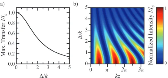
Figure 2.12: a) Maximum normalized power transfer between modes as a function of∆/k. A power transfer of 95% requires ∆/k < 0.459. b) Intensity in an undriven mode coupled to a driven mode at ratek, with phase velocity splitting∆, plotted as a function of dimensionless parameters ∆/k and kz, where z is the position along the waveguide.
achievable fractional power transfer is plotted in Fig. 2.12 a) as a function of∆/k. Fig. 2.12 b) shows Eq. 2.47 plotted as a function of the dimensionless parameters kz and ∆/k.
CHAPTER III
Time-resolved Faraday/Kerr rotation measurements
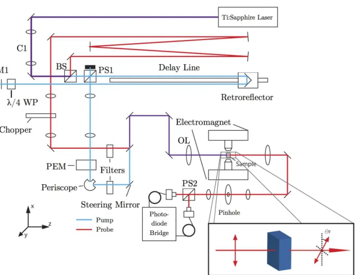
In this chapter, time-resolved Faraday rotation (TRFR) measurement techniques which are used throughout the following chapters are presented. TRFR is a pump-probe measure-ment technique that allows spin dynamics to be investigated with a temporal resolution of a few picoseconds. This level of resolution is achieved by controlling differences in optical path length, so that the shortest resolvable time step is set by the precision with which a mechanical delay line can be positioned. In the following sections, the optical apparatus, laser system, modulation and signal processing scheme, as well as other crucial systems for performing TRFR measurements will be discussed.
3.1
TRFR measurement apparatus
Figure 3.1 shows an overview of the optical system used in TRFR measurements. In this section, the beam path will be described and the important components along the way are discussed. Labels in Fig. 3.1 are referred to throughout the following section when discussing the beam path.
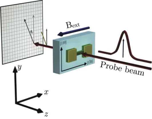
The sample is placed in a Janis ST-300 (transmission) or ST-500 (reflection) helium flow cryostat which maintains a constant temperature within the range of 5 K to room temper-ature. A thermocouple is used to monitor the sample temperature, which is maintained at a constant value by way of an ohmic heater and PID controller. The cryostat is placed
between the poles of an electromagnet which, with the addition of a chilled liquid cooling system, can sustain a field strength of 300 mT at ambient temperature and full duty cycle. Current is driven by a Kepco voltage-controlled current source capable of driving 8 A at up to 40 V, and the set voltage is generated by an auxiliary DAC channel on one of the lock-in amplifiers used in these experiments.
3.1.1 Laser system
We start with the laser system. Optical pulses with a duration of a few picoseconds are generated by means of mode-locking using a Coherent MIRA 900 titanium sapphire laser. The exceptionally wide gain bandwidth (spanning approximately 700-1000 nm) provided by the Ti:sapphire crystal allows for a very large number of simultaneous cavity modes. Mode-locking is achieved by enforcing a phase relationship between some subset of these modes which leads to brief intense pulses when all modes constructively interfere followed by a (relatively) long period during which the modes destructively interfere and no light is emitted. When this phase relationship between the modes is established, the laser is said to be mode-locked. The laser uses a combination of passive Kerr lensing in the Ti:Sapphire crystal and a sophisticated servo loop to initiate and maintain mode locking and control group velocity dispersion in the cavity. In the best-case scenario, the minimum achievable pulse duration is limited by the bandwidth of cavity modes which are successfully mode-locked. In practice, the pulse times are rather longer than the linewidth would suggest, usually due to dispersion in the optical setup. The repetition rate of the laser is set by the total cavity length, which in our case leads to a repetition time of 13.158 ns, or a pulse frequency of 76 Mhz. The MIRA system used here can operate in two modes, somewhat deceptively labeled picosecond mode and femtosecond mode. In picosecond mode, pulse times are approximately 5 picoseconds, while in femtosecond mode pulses of approximately 150 femtoseconds are possible if the laser is well calibrated. The Ti:sapphire crystal in the MIRA 900 is optically pumped by a 10 watt 532 nm beam generated by a Coherent Verdi
V10 laser system. A diode laser emitting at 1064 nm is frequency-doubled to 532 nm in a non-linear crystal composed of lithium triborate to generate the pump beam. When the laser is operating optimally, an average output power of around 2 watts is possible when the pulse center frequency is tuned within the range of 830–850 nm.
3.1.2 Optical beam path
With our optical pulses successfully formed, the beam first passes through a lens pair, labeled C1 in Fig. 3.1, which collimates the beam. It then travels to a beam splitter (BS) which splits the beam into two components. The reflected portion becomes the probe beam (red) and the transmitted component becomes the probe beam (blue). We start by following the pump beam, which immediately passes through a polarizing beam splitter (PS) oriented so that on the first pass the light is fully transmitted. It then enters the delay line, which consists of a retroreflector mounted to a cart which moves along a high-precision guide rail. Light travels down the rail and is reflected back, offset by a small amount such that on the return trip it misses the polarizing beam splitter. It then passes through a quarter wave plate (λ/4), reflects off a mirror (M1) back along its path, and then passes through the quarter wave plate again. When the beam is reflected off M1 its helicity is reversed, so that after the second pass through the quarter wave plate it is traveling back down the delay line with a polarization orthogonal to its original polarization if the quarter wave plate is properly oriented with respect to the incident polarization. It hits the retroreflector again, and then the polarizing beam splitter. Since the beam travels the full length of the delay line twice, this is referred to as a double-pass delay line. The position of the retroreflector can be moved by about 70 cm, so that the total optical path length changes by 2.8 m. We can therefore adjust the time it takes the pump pulse to travel to the sample by about 9 ns. Now, the beam is fully reflected by the polarizing beam splitter. The fact that we have intentionally sent the beam back along its original path can sometimes lead to difficulty maintaining mode locking, as the reflected beam can upset the mode-locking process if it is coupled back into
the laser cavity. The pump beam then passes through a photo-elastic modulator (PEM). This component modulates the incoming beam so that the transmitted beam oscillates from left to right circular polarization at 50 kHz. The PEM serves two purposes in our experiment; first, it allows for lock-in detection methods to be used. Second, by modulating the helicity of the probe beam, the time-averaged injected spin polarization is zero. This prevents the inadvertent introduction of a nuclear polarization due to direct optical pumping. The beam is then filtered to limit the incident pump power. The beam then reflects off a computer-controlled steering mirror which is used to systematically adjust the overlap of the pump and probe beams on the sample. The pump and probe beams are then recombined, pass through a set of manual steering mirrors, and are focused by an objective lens (OL) onto the sample.
When compared to the pump beam path, the probe beam path is relatively simple. After being split off at the first beam splitter (BS), it is reflected off a set of mirrors which are there to roughly equalize the optical path lengths of the probe beam and the pump beam when it is near its maximum path length. The length of this compensating path determines the range of pump-probe delay times ∆t that can be obtained. We typically set this so that the delay range can be adjusted over the range ∆t = −1 to 8 ns. Here, negative delays indicate that the probe beam arrives before the pump. The probe beam is then focused onto an optical chopper used for lock-in detection. It is then filtered, passes through the same set of steering mirrors as the probe, and is focused by the objective lens onto the sample. In Fig. 3.1, the transmitted component of the probe beam is collected, however in some situations it is advantageous to collect the reflected portion of the probe beam instead. The latter case is termed Kerr rotation, while the former is known as Faraday rotation. The collected probe beam is then focused on a pin hole which is used to filter out as much of the scattered pump beam as possible. It then is rotated in a half-wave plate and hits a polarizing beam splitter. The half wave plate is used to adjust the polarization of the probe beam so that it is evenly split at (PS2). A photodiode bridge is then used to measure the difference between