PSoC 4 Prototyping Kit Guide
Doc. #: 001-90711 Rev. **
Cypress Semiconductor
198 Champion Court
San Jose, CA 95134-1709
Phone (USA): +1.800.858.1810
Phone (Intnl): +1.408.943.2600
http://www.cypress.com
Copyrights
© Cypress Semiconductor Corporation, 2014. The information contained herein is subject to change without notice. Cypress Semiconductor Corporation assumes no responsibility for the use of any circuitry other than circuitry embodied in a Cypress product. Nor does it convey or imply any license under patent or other rights. Cypress products are not warranted nor intended to be used for medical, life support, life saving, critical control or safety applications, unless pursuant to an express written agreement with Cypress. Furthermore, Cypress does not authorize its products for use as critical components in life-support systems where a malfunction or failure may reasonably be expected to result in significant injury to the user. The inclusion of Cypress products in life-support systems application implies that the manufacturer assumes all risk of such use and in doing so indemnifies Cypress against all charges.
Any Source Code (software and/or firmware) is owned by Cypress Semiconductor Corporation (Cypress) and is protected by and subject to worldwide patent protection (United States and foreign), United States copyright laws and international treaty provisions. Cypress hereby grants to licensee a personal, non-exclusive, non-transferable license to copy, use, modify, create derivative works of, and compile the Cypress Source Code and derivative works for the sole purpose of creating custom soft-ware and or firmsoft-ware in support of licensee product to be used only in conjunction with a Cypress integrated circuit as speci-fied in the applicable agreement. Any reproduction, modification, translation, compilation, or representation of this Source Code except as specified above is prohibited without the express written permission of Cypress.
Disclaimer: CYPRESS MAKES NO WARRANTY OF ANY KIND, EXPRESS OR IMPLIED, WITH REGARD TO THIS MATE-RIAL, INCLUDING, BUT NOT LIMITED TO, THE IMPLIED WARRANTIES OF MERCHANTABILITY AND FITNESS FOR A PARTICULAR PURPOSE. Cypress reserves the right to make changes without further notice to the materials described herein. Cypress does not assume any liability arising out of the application or use of any product or circuit described herein. Cypress does not authorize its products for use as critical components in life-support systems where a malfunction or failure may reasonably be expected to result in significant injury to the user. The inclusion of Cypress’ product in a life-support sys-tems application implies that the manufacturer assumes all risk of such use and in doing so indemnifies Cypress against all charges.
Use may be limited by and subject to the applicable Cypress software license agreement.
PSoC and CapSense are registered trademarks and PSoC Creator are trademarks of Cypress Semiconductor Corp. All other trademarks or registered trademarks referenced herein are property of the respective corporations.
Flash Code Protection
Cypress products meet the specifications contained in their particular Cypress PSoC Data Sheets. Cypress believes that its family of PSoC products is one of the most secure families of its kind on the market today, regardless of how they are used. There may be methods, unknown to Cypress, that can breach the code protection features. Any of these methods, to our knowledge, would be dishonest and possibly illegal. Neither Cypress nor any other semiconductor manufacturer can guaran-tee the security of their code. Code protection does not mean that we are guaranguaran-teeing the product as ‘unbreakable’. Cypress is willing to work with the customer who is concerned about the integrity of their code. Code protection is constantly evolving. We at Cypress are committed to continuously improving the code protection features of our products.
Safety Information
5
1. Introduction
7
1.1 Kit Contents ...7
1.2 Getting Started...8
1.3 Additional Learning Resources ...8
1.4 Technical Support ...8 1.5 Document Conventions ...8
2. Software Installation
9
2.1 Kit Software ...9 2.2 Install Hardware ...10 2.3 Uninstall Software ...102.4 Open the PSoC 4 Code Example Project in PSoC Creator...11
3. Kit Operation
13
3.1 Connecting the PSoC 4 Prototyping Kit to a Computer ...133.2 CY8CKIT-049-4xxx USB COM Port ...14
3.2.1 Configuring the COM Port...15
3.3 Programming the CY8CKIT-049-4xxx Kit ...17
3.3.1 Programming a CY8CKIT-049-4xxx Project Using MiniProg3 ...18
3.3.2 Programming a CY8CKIT-049-4xxx Project Using the Bootloader ...21
3.4 USB-UART Default Settings ...27
4. Hardware
28
4.1 Board Details ...284.2 Theory of Operation ...29
4.3 Functional Description ...29
4.3.1 Power Supply System ...29
4.3.2 Board Separation (Snapping)...30
4.3.3 Header Connections ...30
4.3.4 User and Passive Inputs ...34
5. Example Projects
37
5.1 Bootloader Base Example Project ...375.2 Bootloadable Example Project...38
5.3 Creating a New Bootloadable Project ...39
5.4 Adapting Projects from 100 Projects in 100 Days ...42
5.4.1 LED Blinky (Project #067) ...42
6. USB-Serial Configuration
51
6.1 USB-Serial Resources... 51
6.2 USB-Serial Configuration Utility... 51
6.2.1 Connecting to a USB-Serial Device ... 52
6.2.2 Configuring a Serial Port... 53
6.2.3 Configuring GPIOs... 56
6.2.4 Additional Features of the USB-Serial Device ... 57
A. Appendix
58
A.1 CY8CKIT-049-4xxx Schematics ... 58Regulatory Compliance
The CY8CKIT-049-4xxx Prototyping Kit is intended for use as a development platform for hardware or software in a laboratory environment. The board is an open system design, which does not include a shielded enclosure. This may cause interference to other electrical or electronic devices in close proximity. In a domestic environment, this product may cause radio interference. In such cases, you may be required to take adequate preventive measures. In addition, this board should not be used near any medical equipment or RF devices.
Attaching additional wiring to this product or modifying the product operation from the factory default may affect its performance and cause interference with other apparatus in the immediate vicinity. If such interference is detected, suitable mitigating measures should be taken.
The CY8CKIT-049-4xxx Prototyping Kit, as shipped from the factory, has been verified to meet with requirements of CE as a Class A product.
The CY8CKIT-049-4xxx contains electrostatic discharge (ESD) sensitive devices. Electrostatic charges readily accumulate on the human body and any equipment, and can discharge without detection. Permanent damage may occur on devices subjected to high-energy discharges. Proper ESD precautions are recommended to avoid performance degradation or loss of functionality. Store unused CY8CKIT-049-4xxx boards in the protective shipping package.
End-of-Life/Product Recycling
This kit has an end-of life five years from the date of manufacture mentioned on the back of the box. Contact your nearest recycler for discarding the kit.
General Safety Instructions
ESD Protection
ESD can damage boards and associated components. Cypress recommends that you perform procedures only at an ESD workstation. If such a workstation is not available, use appropriate ESD protection by wearing an antistatic wrist strap attached to the chassis ground (any unpainted metal surface) on your board when handling parts.
Handling Boards
CY8CKIT-049-4xxx boards are sensitive to ESD. Hold the board only by its edges. After removing the board from its box, place it on a grounded, static-free surface. Use a conductive foam pad if available. Do not slide board over any surface.
Thank you for your interest in the PSoC® 4 CY8CKIT-049-4xxx family of prototyping kits. The proto-typing kit is designed as an easy-to-use and inexpensive protoproto-typing platform for users wishing to rapidly develop products using the PSoC 4 families and use the unique flexibility of the PSoC 4 architecture. Designed for flexibility, these kits offer an open footprint breakout board to maximize the end utility of the PSoC 4 device. These kits provide a low-cost alternative to device samples while providing a platform to easily develop and integrate the PSoC 4 device into your end system. In addition, the board includes the following features:
■ Onboard CMOD capacitors to enable CapSense® development
■ A bypass capacitor to ensure the high quality ADC conversions
■ An LED to provide feedback
■ A push button to provide a simple user input and trigger the bootloader programming mode The CY8CKIT-049-4xxx development kit also supports the Cypress USB-Serial CY7C65211 Full-Speed USB controller that enables PC connectivity and serial interfaces, such as UART, USB-I2C, USB-SPI, and USB-GPIO. The development kit includes a Cypress USB-Serial controller used to bootload the target PSoC 4 device. The PSoC 4 prototyping board is breakable, allowing you to separate the USB-Serial board from the PSoC 4 board.
This kit supports either 5 V or 3.3 V power supply voltages. The device can be programmed using the bootloader or the Cypress MiniProg3 programmer. The PSoC 4 Prototyping Kit supports boards based on the 4100 and 4200 device families, delivering a programmable platform for a wide range of embedded applications at a very low cost. The PSoC 4 is a scalable and reconfigurable platform architecture for a family of mixed-signal programmable embedded system controllers with an ARM® Cortex™-M0 CPU. It combines programmable and reconfigurable analog and digital blocks with flex-ible automatic routing.
1.1
Kit Contents
This kit contains only the PSoC 4 Prototyping Kit, either the 4100 or 4200 series device. Figure 1-1. PSoC 4 CY8CKIT-049-4xxx Prototyping Kit
1.2
Getting Started
This user guide helps you to get acquainted with the PSoC 4 Prototyping Kit. The Software Installation chapter on page 9 describes the installation of the PSoC Creator software. The Kit Operation chapter on page 13 explains how to program the kit using a bootloader or a MiniProg3. The Hardware chapter on page 28 details the hardware operation of the kit. The Example Projects chapter on page 37 and USB-Serial Configuration chapter on page 51 walk you through making projects and configuring the USB-Serial device on the kit. The Appendix on page 58 pro-vides the schematics, pin assignment, and bill of materials (BOM).
1.3
Additional Learning Resources
For more information on PSoC, see the following links:
■ www.cypress.com/psoc ■ www.cypress.com/psoc4 ■ www.cypress.com/psoccreator ■ www.cypress.com/CY8CKIT-049-41xx ■ www.cypress.com/CY8CKIT-049-42xx ■ www.cypress.com/CY8CKIT-042 ■ www.cypress.com/go/usbserial
1.4
Technical Support
For assistance, go to our support web page, or contact our customer support: Phone (USA): +1(800) 541-4736 extension 2
Phone (International): +1 (408) 943-2600, extension 2
1.5
Document Conventions
Table 1-1. Document Conventions for Guides
Convention Usage
Courier New Displays file locations, user entered text, and source code:
C:\...cd\icc\
Italics Displays file names and reference documentation:
Read about the sourcefile.hex file in the PSoC Designer User Guide. [Bracketed, Bold] Displays keyboard commands in procedures:
[Enter] or [Ctrl] [C] File > Open Represents menu paths:
File > Open > New Project
Bold Displays commands, menu paths, and icon names in procedures: Click the File icon and then click Open.
Times New Roman Displays an equation:
2 + 2 = 4
2.1
Kit Software
The PSoC 4 Prototyping Kit does not require installation, but it is recommended that you install the following content:
■ PSoC Creator™
■ EZ-USB Software Development Kit (SDK)
To install PSoC Creator, download the installer from the download table on the PSoC Creator web page and install it.
1. Run the installer and select the folder to install the PSoC Creator files. Choose the directory and click Next.
2. Select the Installation type and click Next. Figure 2-1. PSoC Creator Installation
3. Accept the Software License Agreement. After the installation is complete, the software is avail-able at the following location: <InstallDirectory>\Cypress\PSoC Creator\<version>. 4. To install the USB-Serial SDK, download the installer from the web page and run it.
5. Run the installer and select the folder to install the USB-Serial SDK files. Choose the directory and click Next.
Figure 2-2. Select Installation Folder for PSoC Creator
6. Accept the Software License Agreement by selecting I Agree and then click Next. After the installation is complete, the following software tools are installed on your computer:
■ USB-Serial Configuration Utility
■ USB-Serial Test Utility
2.2
Install Hardware
There is no additional hardware installation required for this kit.
2.3
Uninstall Software
To uninstall the software, do one of the following:
■ Go to Start > All Programs > Cypress > Cypress Update Manager > Cypress Update Man-ager, and then select Uninstall.
2.4
Open the PSoC 4 Code Example Project in PSoC Creator
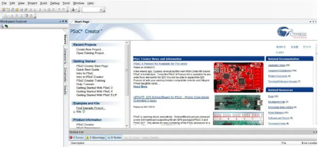
1. Launch the PSoC Creator software from the Start menu.Figure 2-3. PSoC Creator Start Page
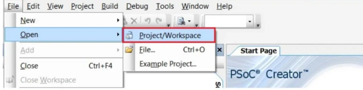
2. Open the example project from the Start Page. Click File > Open > Project/Workspace, and open the example project downloaded from the kit page.
Figure 2-4. Open Project/Workspace
The example project opens and displays the project files in the Workspace Explorer. The work-space includes two sample projects linked in the Workspace Explorer. Subsequent sections of this user guide show how to build, program, and understand the example projects supplied with this kit.
The PSoC 4 Prototyping Kit is simplistic in design and focuses on providing you with complete access to develop applications using the PSoC 4 device family. The development kit supports a number of onboard functions such as an LED, push button, through-hole connections, USB-Serial connectivity to the PC, and a breakable board design to separate the two target boards.
Figure 3-1. PSoC 4 Prototyping Kit
3.1
Connecting the PSoC 4 Prototyping Kit to a Computer
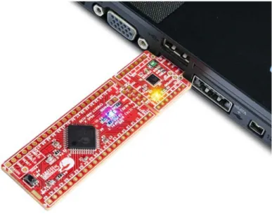
To use the PSoC 4 Prototyping Kit, you need to connect the kit to a target PC. The kit is designed to be connected to the computer through USB. The USB connector will provide power to the target boards and enable serial communication. CY8CKIT-049-4xxx implements a PCB-based USB con-nector that makes connections to the USB port when plugged in. The amber LED turns on when the board is plugged into the port to indicate power.
Figure 3-3. PSoC 4 Prototyping Kit Connected to the Computer
3.2
CY8CKIT-049-4xxx USB COM Port
When you connect CY8CKIT-049-4xxx to the PC over a USB interface, it enumerates as a COM port device under the Device Manager window in Windows OS. Often, the COM port number will be higher than any existing COM port value. For example, in the following image the CY8CKIT-049-4xxx enumerates as COM37.
Figure 3-4. CY8CKIT-049-4xxx USB COM Port in Device Manager
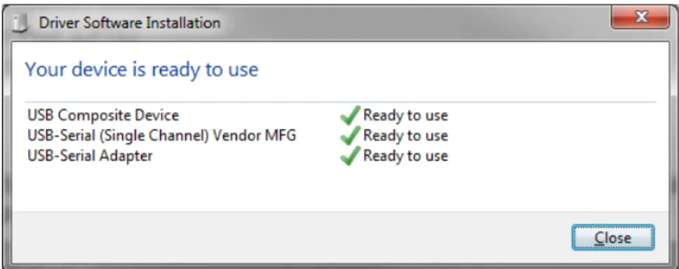
When connecting your CY8CKIT-049-4xxx to a computer for the first time or to any new USB port, it may take a moment to enumerate because the computer will complete an online check for the latest drivers.
Figure 3-6. Driver Software Installation Complete
3.2.1
Configuring the COM Port
Different USB COM devices are connected to different USB ports and the PC assigns COM port val-ues to those devices. As more devices are connected, the COM port valval-ues will continue to increase. Some applications require the COM port to be less than 10, such as ‘COM10’. In the fol-lowing examples, the Bootloader Host utility requires a COM port number below 10.
To change the assigned COM port number, do the following: 1. Open the Device Manager from the Control Panel window. Figure 3-7. Windows Device Manager
2. On the Device Manager window, under Ports (COM and LPT), right-click on the COM port cre-ated by the CY8CKIT-049-4xxx kit and select Properties.
Figure 3-8. Configuring COM Port for CY8CKIT-049-4xxx
3. Select the Port Settings tab and click the Advanced… button. Figure 3-9. Configuring COM Port Settings for CY8CKIT-049-4xxx
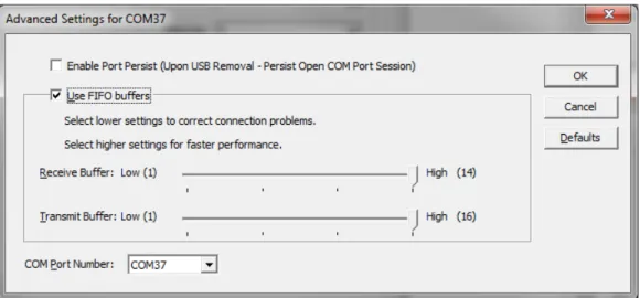
4. Click the COM Port Number drop-down menu and select an available COM port; click OK. Some COM ports will have the indicator (in use). Select a port that does not have this identifier. Figure 3-10. Configuring COM Port Settings for CY8CKIT-049-4xxx
The Device Manager window will then display the new COM port value. In the following image, the value changed from COM37 to COM2.
Figure 3-11. Renamed COM Port for CY8CKIT-049-4xxx in Device Manager
3.3
Programming the CY8CKIT-049-4xxx Kit
The CY8CKIT-049-4xxx kits are pre-programmed with firmware containing a bootloader. Therefore, there are two methods of programming the onboard PSoC 4 device:
1. Perform UART bootload programming of the PSoC 4 device using the USB-Serial device as a USB-UART bridge.
2. Use a CY8CKIT-002 MiniProg3 to program and debug the target device directly.
Note that as long as the PSoC 4 device on the kit contains the bootloader, either method of program-ming can be used. If a project without a bootloader is programmed onto the PSoC 4, then only the second method may be used until the PSoC 4 device is reprogrammed with a bootloader. In other words, any project can be programmed using the MiniProg3 programmer, but only a bootloadable project can be bootloaded using the first method.
See the following sections for an example of a bootloader project and a bootloadable project. See application note AN73854 for additional details on bootloading.
3.3.1
Programming a CY8CKIT-049-4xxx Project Using MiniProg3
To use MiniProg3 for programming, connect wires or a 5-pin 100-mil spaced header to the program-ming header on the CY8CKIT-049-4xxx board. The programprogram-ming header is a 5-pin header indicated on the silkscreen and is labeled ‘PROG’. This connector is oriented to mate directly with MiniProg3's 5-pin header. The CY8CKIT-049 supports both power cycle and reset programming modes.
Figure 3-12. Connecting CY8CKIT-049-4xxx to MiniProg3
Note: CY8CKIT-002 MiniProg3 is not part of the PSoC 4 Prototyping Kit contents and can be pur-chased from the Cypress Online Store.
The following images show the pinout for MiniProg3 and the connections on CY8CKIT-049-4xxx. Figure 3-13. Pinout for MiniProg3
Figure 3-14. CY8CKIT-049-4xxx Connections for MiniProg3
The code examples described in this section show how to bootload new projects into PSoC 4 and create bootloader and bootloadable projects. To access the kit examples, download the examples from the kit web page.
The initial example shows how to program the kit with just a bootloader using MiniProg3. Note that the kit is pre-programmed with a project containing a bootloader, so this step is not necessary to change the application firmware.
1. Launch PSoC Creator from the Start menu. Figure 3-15. PSoC Creator Start Page
2. Open the example project workspace from the Start Page. Select File > Open > Project/Work-space.
Figure 3-16. Opening the Project in PSoC Creator
The example opens and displays the project files in the Workspace Explorer. The workspace includes two sample projects linked in the Workspace Explorer - a bootloader project and a boot-loadable project.
4. Right-click the UART_Bootloader project and select Set As Active Project. Figure 3-17. Setting Example Project as Active Project in Workspace Explorer
5. Select Build > Build UART_Bootloader. Figure 3-18. Building the Project
6. Connect MiniProg3 to the CY8CKIT-049-4xxx prototyping board. 7. Select Debug > Program.
Figure 3-19. Programming the CY8CKIT-049-4xxx
The Select Debug Target window opens. Figure 3-20. Debug Target Window
8. Click Port Settings, set the connector to 5 pin, and then click OK.
9. Click Port Acquire to detect the target device, click Connect, and then click OK.
PSoC Creator programs the target. When programming is complete, the PSoC 4 will contain the bootloader but not any application code.
3.3.2
Programming a CY8CKIT-049-4xxx Project Using the Bootloader
The following example shows how to bootload a project into the PSoC 4 with the USB-Serial device, using the Bootloader Host. To use this method, the PSoC 4 device must contain the bootloader and
the project must be configured as bootloadable. This is the default programming method for new users.
The following steps use the example project downloaded from the kit web page. 1. Launch PSoC Creator from the Start menu.
2. From the Start Page, select File > Open > Project/Workspace.
3. Open the project by navigating to the example project downloaded from the kit page. Figure 3-21. Open the Project
The example project opens and displays the project files in the Workspace Explorer. The work-space includes two sample projects linked in the Workwork-space Explorer.
4. In the Workspace Explorer, right-click the Bootloadable Blinking LED project and select Set As Active Project.
Figure 3-22. Set the Example Project as Active Project
The bootloadable project must be associated with the bootloader project's HEX and ELF files. This will ensure that the firmware code mapping aligns with the code on the target device. 5. Under the 'Bootloadable Blinking LED' example project, double-click the 'TopDesign.cysch' file to
open the schematic view. Select the tab for the Bootloadable Project schematic page if it is not already selected.
Figure 3-23. Open Schematic View
6. In the schematic view, right-click the Bootloadable component and select Configure. Figure 3-24. Configure the Bootloader Component
7. In the configuration window, select the Dependencies tab and click the Browse button to point to the HEX and ELF files generated when the bootloader project was built in Programming a CY8CKIT-049-4xxx Project Using MiniProg3 on page 18; click OK. The file paths (assuming the 42xx kit) will appear as follows:
[Download_Directory]\SCB_Bootloader_42XX\SCB_Bootloader_42XX\UART_Bootl oader.cydsn\CortexM0\ARM_GCC_473\Debug\UART_Bootloader.HEX
[Download_Directory]\SCB_Bootloader_42XX\SCB_Bootloader_42XX\UART_Bootl oader.cydsn\CortexM0\ARM_GCC_473\Debug\ UART_Bootloader.ELF
Figure 3-25. Configure Dependencies for Bootloader Component
8. Select Build > Build Bootloadable Blinking LED. Figure 3-26. Build the Project
9. Connect the CY8CKIT-049-4xxx prototyping board to the PC. When connecting the kit to the port, depress the SW1 button as it is plugged in.
You will notice that the LED begins to blink rapidly; this indicates that the PSoC 4 is in 'Bootloader Mode' and is ready to be loaded with the latest firmware. This must be done each time you boot-load the PSoC 4.
Figure 3-27. Launch Bootloader Host Tool
The Bootloader Host tool opens. Figure 3-28. Bootloader Host Tool
11. Click Filters and select the Show UART Devices option from the Port Filters window and click
Figure 3-29. Port Filters
The Bootloader Host tool will now display all of the available UART based COM ports. 12.Click the COM port from the list of available ports and enter the UART configuration such as
Baud Rate, Data Bits, Stop Bits, and Parity for the USB-UART configuration on the USB-Serial device.
The default values for the UART are: 115200 baud rate, 8 data bits, 1 stop bit, and no parity. 13.Click File > Open and navigate to the Bootloadable_Blinking_LED.cyacd file generated in the
CortexM0 folder in your project directory, and click Open. Figure 3-30. Opening the Generated File
14.Click the Program button to flash the part with your new application code.
The status window provides output message and a status bar indicates the programming prog-ress. When bootloading is complete, your application executes with the latest version of the application code.
Figure 3-31. Program the Device With Application Code
Note that the blinking LED firmware created in this section could have been programmed into the PSoC 4 using a MiniProg3 instead of using bootloading if required. In PSoC, a bootloadable project always contains both the application as well as the complete bootloader. Therefore, if the HEX file from the Bootloadable Blinking LED project were to be programmed using a MiniProg3, the resulting device would still be bootloadable.
3.4
USB-UART Default Settings
The default configuration of the USB-Serial device on the CY8CKIT-049-4xxx prototyping kit is the USB-UART mode. The CY8CKIT-049-4xxx also enables a default UART connection between the USB-Serial device and the PSoC 4. This connection is indicated by two parallel 4-pin headers in the middle of the board. The default pin connections are shown in Table 3-2.
Figure 3-32. UART Pin Connections on CY8CKIT-049-4xxx
The USB-Serial device provides the PSoC 4 device with an interface to a PC. The USB-Serial device enumerates as a COM port to allow any terminal software to be used to communicate with the PSoC 4. To use the USB-UART functionality in the COM terminal software, select the corre-sponding COM port. Note that if the USB-Serial device board is separated from the PSoC 4 board, you will still be able to use the USB-Serial device to communicate with any UART device using the 4-pin header.
The USB-Serial device is by default configured as a USB-UART device with the following specifica-tions. Default values are shown in bold.
Table 3-1. Pin Mapping for USB Serial Port and PSoC 4 UART USB Serial UART PSoC 4 UART
TX P4.0 (RX)
RX P4.1 (TX)
GND GND
VDD VDD
Table 3-2. USB-UART Parameters
Parameter Supported Values
Baud Rate 100, 200, 300, 600, 1200, 2400, 4800, 9600, 14400, 19200, 38400, 56000, 57600, 115200, 230400, 460800, 921600, 1000000, 3000000 Type 2 pin, 4 pin, 6 pin
Data Bits 7 bits, 8 bits Stop Bits 1 bit, 2 bits
Parity None, Odd, Even, Mark, Space Drop Packets on RX error Disabled, Enabled
Disable CTS and DSR pull-up during
4.1
Board Details
The PSoC 4 Prototyping Kit consists of the following blocks:
■ PSoC 4 device
■ PSoC 4 header ports J1 and J2
■ USB-Serial device
■ USB-Serial header ports J5 and J6 (GPIO)
■ UART connection J3 and J4 (SCB and GPIO)
■ PCB USB connector
■ One amber LED (Power)
■ One blue LED (User)
■ Push button
■ External reference capacitor (ADC Bypass)
■ CapSense and shield capacitors (CMOD and CTANK)
■ Programming connector
■ Perforated 'snappable' board design Figure 4-1. CY8CKIT-049-4xxx Pin Details
4.2
Theory of Operation
PSoC 4 is a new generation of programmable system-on-chip device from Cypress for embedded applications. It combines programmable analog, programmable digital logic, programmable I/O, and a high-performance ARM Cortex-M0 core. With PSoC 4, you can create the combination of peripher-als required to meet your application's specifications.
The PSoC 4 Prototyping Kit features an onboard USB-Serial device, which communicates to a PC through USB to provide serial communication support and serial port debugging.
The PSoC 4 Prototyping Kit has a user LED and a power status LED. This kit includes a button that connects to the PSoC 4 device, which can be used to develop applications. This button is also used to enable the onboard bootloader. The PSoC 4 pins are brought out onto headers J1 to J2 on the kit and support 100-mil breadboard spacing.
The PSoC 4 Prototyping Kit can be powered from USB or an external power supply. The input volt-age is either 5 V from USB or a variable supply from an external source.
Figure 4-2. CY8CKIT-049-4xxx Functional Block Diagram
4.3
Functional Description
4.3.1
Power Supply System
The power supply system on this board is dependent on the source of the power. For most applica-tions, you can use the 5 V supply from the USB connection to power the system. You can also con-nect an external power supply to the board for low-voltage applications. The kit supports the following connections:
■ 5 V from the PCB USB
■ 1.8-5 V from a regulated supply connected to VDD
It is important to understand that this prototyping kit does not have any onboard ESD protection cir-cuitry. Therefore, the power source for the CY8CKIT-049-4xxx must be of a high quality to ensure that the board is protected from any over-current conditions and swapped-power connections.
4.3.1.1
Measure PSoC 4 Current Consumption
You can measure the current consumption of the PSoC 4 device by using one of these methods: Method 1:
1. Separate the USB-Serial board by 'snapping' the perforated edge between the two boards. 2. Power the remaining prototyping board via any of the VDD terminals.
3. Place an ammeter in series with the VDD connection to measure the current consumption. Method 2:
1. Remove the resistor R6 and install a 2-pin jumper in the supplied holes of J4.
2. Connect an ammeter across the 2-pin jumper to measure the current to the PSoC 4 device. This method can be used either with USB power or with power supplied to one of the VDD pins.
4.3.2
Board Separation (Snapping)
CY8CKIT-049-4xxx supports both the PSoC 4 and USB-Serial boards. To separate the two boards for testing or development, break the two boards apart at the built-in perforated edge.
The easiest method of separating the two boards is to place the kit on the edge of a table, where the edge of the table is directly below the perforated edge and the smaller USB-Serial device is off the table edge. Press gently on the USB-Serial board and snap the two boards apart. If any material is removed from the edge of the boards, use sheers to clean up the edge of the kit.
Figure 4-3. CY8CKIT-049-4xxx Broken as Two Parts
4.3.3
Header Connections
The CY8CKIT-049-4xxx Prototyping Kit supports a number of unpopulated headers on both the USB-Serial and the PSoC 4 boards.
4.3.3.1
Functionality of the J1 and J2 Headers (PSoC 4)
The main PSoC 4 board contains two dual-inline headers (J1 and J2). These headers are both 1×22-pin headers and include all of the I/O available on the PSoC 4 devices. These headers support all of the available ports, GND, VDD, and connections to passive elements and user-input devices. The J1 and J2 headers support 100-mil spacing, so you can solder the male connectors to connect the CY8CKIT-049-4xxx to any development breadboard.
Figure 4-4. J1 and J2 Headers
Table 4-1. J1 Header Pin Details
PSoC 4 GPIO Header (J1)
Pin Signal Description
Pin Signal Description J1_01 P4.0 GPIO J1_02 P4.1 GPIO J1_03 P4.2 GPIO/CMOD J1_04 P4.3 GPIO/CTANK J1_05 P0.0 GPIO J1_06 P0.1 GPIO J1_07 P0.2 GPIO J1_08 P0.3 GPIO J1_09 P0.4 GPIO J1_10 P0.5 GPIO J1_11 P0.6 GPIO J1_12 P0.7 GPIO/SW1 J1_13 P1.0 GPIO J1_14 P1.1 GPIO J1_15 P1.2 GPIO J1_16 P1.3 GPIO J1_17 P1.4 GPIO J1_18 P1.5 GPIO J1_19 P1.6 GPIO/LED1
J1_20 P1.7 GPIO/SAR Bypass (EXT_VREF) J1_21 GND Ground
4.3.3.2
Functionality of J3 and J5 Headers (PSoC 4 to USB-Serial)
Both the USB-Serial and the PSoC 4 prototyping boards each contain a 1×4-pin header. This header provides a physical connection between the two devices. Specifically, the connection includes the UART (RX and TX), VDD, and GND connections between the two devices. When the boards are separated, this physical connection is broken.
Figure 4-5. J3 and J5 Headers Table 4-2. J2 Header Pin Details
PSoC 4 GPIO Header (J2)
Pin Signal Description
J2_01 VDD Power J2_02 GND Ground J2_03 RESET Reset J2_04 P3.3 GPIO/SWDCLK J2_05 P3.2 GPIO/SWDIO J2_06 P3.7 GPIO J2_07 P3.6 GPIO J2_08 P3.5 GPIO J2_09 P3.4 GPIO J2_10 P3.3 GPIO/SWDCLK J2_11 P3.2 GPIO/SWDIO J2_12 P3.1 GPIO J2_13 P3.0 GPIO J2_14 P2.7 GPIO J2_15 P2.6 GPIO J2_16 P2.5 GPIO J2_17 P2.4 GPIO J2_18 P2.3 GPIO J2_19 P2.2 GPIO J2_20 P2.1 GPIO J2_21 P2.0 GPIO J2_22 GND Ground
Figure 4-6. UART Connection to PSoC 4
4.3.3.3
Functionality of J6 and J7 Headers (USB-Serial)
The USB-Serial board contains two dual-inline headers (J6 and J7). These headers are both 1x7-pin headers and include all of the GPIO and SCB connections. These headers support all of the avail-able ports, GND, VDD, and connections to passive elements and user-input devices.
The J6 and J7 headers support 100-mil spacing, so you can solder the male connectors to connect the USB-Serial board to any development breadboard.
Figure 4-7. J6 and J7 Connectors Table 4-3. Pin Details of J3 Header
PSoC 4 to USB-Serial Header (J3)
Pin Signal Description
J3_01 VDD Power J3_02 GND Ground J3_03 P4.0 UART RX J3_04 P4.1 UART TX
Table 4-4. Pin Details of J5 Header
USB-Serial to PSoC 4 Header (J5)
Pin Signal Description
J4_01 VDD Power J4_02 GND Ground J4_03 SCB.0/GPIO_6 UART TX J4_04 SCB.4/GPIO_5 UART RX
4.3.4
User and Passive Inputs
4.3.4.1
Push Button
The main PSoC 4 board contains a single push button connected to the P0.7 pin on the PSoC 4 device. This button can be used for general user inputs and for triggering the bootloader for pro-gramming.
Figure 4-8. Push Button on the Board Table 4-5. Pin Details of J6
USB-Serial Comm/GPIO Header (J6)
Pin Signal Description
Pin Signal Description J5_01 VDD Power J5_02 GND Ground J5_03 S SEL Mode 0-6 J5_04 MISO/SCL Mode 0-6 J5_05 MOSI/SDA Mode 0-6 J5_06 SCLK Mode 0-6 J5_07 SCB.5/GPIO_7 Mode 0-6
Table 4-6. Pin Details of J7
USB-Serial GPIO Header (J7)
Pin Signal Description
Pin Signal Description J6_01 GND Power J6_02 GPIO.0 Ground J6_03 GPIO.1 Reset J6_04 GPIO.8 GPIO J6_05 GPIO.9 GPIO J6_06 GPIO.10 GPIO J6_07 GPIO.11 GPIO
Figure 4-9. Push Button Schematic
4.3.4.2
CY8CKIT-049-4xxx LEDs
CY8CKIT-049-4xxx contains two LEDs: the amber LED, which indicates the board is power applied and the blue LED that is directly connected to the PSoC 4 device through the pin P1.6. The blue LED is also used to indicate the bootloader mode by rapidly blinking. The power LED is on the USB-Serial board; if the boards are separated, the PSoC 4 section does not consume current through the power LED.
Figure 4-10. Power LED
Figure 4-11. User LED
Figure 4-13. User LED Connection
4.3.4.3
System Capacitors
The three capacitors on the CY8CKIT-049-4xxx prototyping kit enable proper development of ADC and CapSense example projects. These capacitors are the following:
■ A SAR ADC bypass capacitor: Required for proper sampling at high frequencies,
■ Two CapSense capacitors (CMOD and CTANK): Required for proper CapSense functionality. Figure 4-14. System Capacitors Circuit Diagram
This section describes how to use the example project included with the kit and how to develop cus-tom bootloadable example projects for new applications.
5.1
Bootloader Base Example Project
The CY8CKIT-049-4xxx prototyping board is pre-programmed with a simple blinking LED example project. This example project uses a PWM to slowly blink an LED. Included in the application project is the Bootloader Base project. The Bootloader code is detailed in the UART_Bootloader project available on the kit web page.
In the bootloader example, the device rapidly blinks an LED when the bootloader is active, provides UART communication support for bootloading, and reads the state of the switch (SW1). You can observe the state of the board by noticing the rate at which the LED blinks. The bootloader is acti-vated when you plug in the CY8CKIT-049-4xxx while pressing the SW1 button. The bootloader reads the state of this button during power-up. If the button is not pressed, the bootloader jumps to the user's application code. If the button is pressed, then the bootloader waits for a new application to be transferred. While the bootloader waits for the new application, it rapidly blinks the onboard blue LED.
Note that the bootloader project is fully customizable, so you can use different methods for entering the bootloader mode, and different feedback mechanisms. For example, you can change the project so that it waits at power-up for a specified amount of time for a new application to be loaded rather than through the use of a button press. All resources of the PSoC are available for use by the boot-loader project.
Figure 5-1. UART Bootloader
The Bootloader Base Project includes the source code in the main.c and the UART_Btld.c files, which support bootloading the PSoC 4 device. The source code is available for reference, but is not necessary to create bootloadable applications.
5.2
Bootloadable Example Project
The example in Programming a CY8CKIT-049-4xxx Project Using the Bootloader on page 21
showed how to bootload the application code for a blinking LED project into the device using the USB-Serial controller.
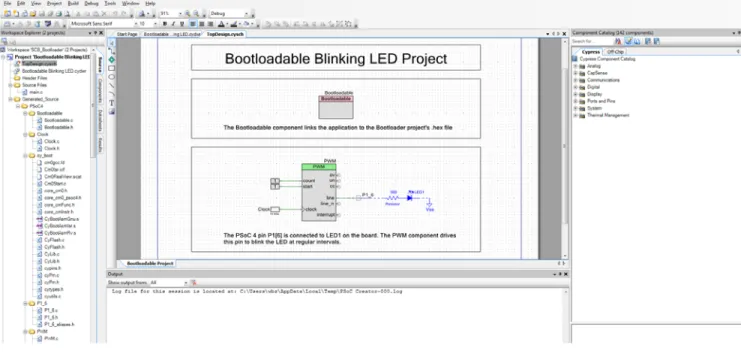
In the bootloadable example project, the following components are used:
■ Bootloadable
■ PWM
■ Clock
■ Digital Output Pin
■ Digital Constants (logic HIGH/LOW)
■ Off-Chip Components (external resistor, LED, and Vss)
In this example project, the PWM component is used to drive an output on a pin connected to the user LED. The bootloadable component is placed to ensure that your application code is correctly mapped to the target PSoC 4 bootloader flash-space mapping.
For more information on how to bootload this project into the base board using the USB-Serial and the USB-Serial Configuration Utility, see the Kit Operation chapter on page 13.
Figure 5-2. Bootloadable Blinking LED Project
5.3
Creating a New Bootloadable Project
To create a new bootloadable project, do the following:
1. On the Start Page of PSoC Creator, click Create New Project. 2. On the New Project window, select an Empty PSoC 4 Design.
3. Click the + button next to Advanced, enter a name for the project, and select a workspace. You can either add the new project to an existing workspace or create a new one.
4. Set the device to the PSoC 4 device on your 049-4xxx. For example, the CY8CKIT-049-42XX kit requires the CY8C4245AXI-483 device.
5. Set the Application Type as Bootloadable. 6. Click OK.
Figure 5-3. Creating a New Bootloadable Project
PSoC Creator generates a new project.
7. Navigate to the schematic view to place your components (double-click on the .cysch file from the project in Workspace Explorer).
Select the Page 1 tab in the schematic if it is not already selected. The key component that must be added is the Bootloadable component, which is used to generate the bootloadable application code.
Figure 5-4. Bootloadable Project Schematic
8. Double-click the Bootloadable component to configure the selections.
The selections must be the same as those in the example project. Refer to Programming a CY8CKIT-049-4xxx Project Using the Bootloader on page 21.
Figure 5-5. Configure Bootloadable Component
9. Click the Dependencies tab to select theHEX and ELF files from the UART Bootloader project included with the kit.
You must always point your bootloadable project to a base bootloader project. The bootloader project can be in the same workspace as your bootloadable project, but this is not necessary. This example project uses the default application shipped with CY8CKIT-049-4xxx.
Figure 5-6. Specifying the References
11. After the project builds without errors, follow the steps shown in Programming a CY8CKIT-049-4xxx Project Using the Bootloader on page 21 to bootload the new code into the target using the Bootloader Host application.
This example does not have any source code, but is a base example project. Follow the steps in the next examples to add functionality to this base project.
5.4
Adapting Projects from 100 Projects in 100 Days
As part of the CY8CKIT-042 PSoC 4 Pioneer Kit release, Cypress provided 100 example projects in 100 days. This section shows you how to import projects to the CY8CKIT-049-4xxx kit that were developed for the CY8CKIT-042 Pioneer Kit on the 100 Projects in 100 Days forum.
Element14 Web Page - 100 projects in 100 days
5.4.1
LED Blinky (Project #067)
The following example explains how to import a project into your workspace and target the CY8CKIT-049-4xxx development kits. This example is adapted from the following project on the 100 Projects in 100 Days forum: PSoC 4 Pioneer Kit Community Project#067 - PSoC 4 Getting Started Lab 1 (LED Blinky)
1. Download the example project from the link provided.
2. In PSoC Creator, click Open Existing Project from the StartPage and navigate to the project to open it.
Figure 5-7. Open Existing Project From PSoC Creator
3. On the Workspace Explorer window, right-click the project and select Build Settings. Figure 5-8. Specifying the Build Settings for the Project
4. Under Code Generation, change the Application Type to Bootloadable from the drop-down list. 5. Click Apply and then click OK.
Figure 5-9. Build Settings for the Project
6. Open the schematic view by double-clicking the .cysch file from the Workspace Explorer window. Select the Page 1 tab in the schematic if it is not already selected.
Figure 5-10. Opening the Schematic View
7. Drag and drop the Bootloadable component into the schematic window from the Component Catalog under System.
Figure 5-11. Schematic View
8. Double-click the Bootloadable component to configure the selections. Figure 5-12. Configuring the Bootloadable Component
9. Click the Dependencies tab to select the .hex and .elf file from the UART_Bootloader project included with the kit.
You must always point your bootloadable project to a base bootloader project. The bootloader project can be in the same workspace as your bootloadable project, but this is not necessary. This project uses the default application shipped with CY8CKIT-049-4xxx.
Figure 5-13. Configuring the Bootloadable Component Dependencies
11. Select Build > Build {Project Name} to build the project. Figure 5-14. Building the Project
12.Connect the CY8CKIT-049-4xxx kit to the PC while pressing the SW1 button. This puts the device into the bootloader mode.
13.From the PSoC Creator menu, select Tools > Bootloader Host to open the Bootloader Host Util-ity.
14.Connect to the COM port and make your port configurations. See Programming a CY8CKIT-049-4xxx Project Using the Bootloader on page 21for more information.
Figure 5-15. Bootloader Host Configuration
15.Click the Open File button and navigate to the bootloadable project's .cyacd file. Typically, the file path is [Project Path]\Lab 1 Blink.cydsn\CortexM0\ARM_GCC_473\Debug.
16.Click Program.
When the firmware is programmed, observe that the LED flashing rate has changed. You can go back into your example project and modify the value in the CyDelay function to change the fre-quency of the LED flashing.
5.4.2
Using the USB-Serial as a USB-UART Bridge (Project#004)
The following example was adapted from the following project on the 100 Projects in 100 Days forum: PSoC 4 Pioneer Kit Community Project#004 - USB-UART Utility
1. Download the example project from the 100 Projects in 100 Days forum link provided. 2. Click Open Existing Project from the Start Page and navigate to the project to open it. 3. On the Workspace Explorer window, right-click on the project and select Build Settings.
Because this project was originally set as a Normal application type, you will need to change it to
Bootloadable.
4. Under Code Generation, change the Application Type, select the drop-down menu and click
Bootloadable.
5. Click Apply and then click OK.
6. Open the schematic view by double-clicking the .cysch file from the Workspace Explorer window. Select the Page 1 tab in the schematic if it is not already selected.
7. Drag and drop the Bootloadable component into the schematic window from the Component Catalog under System.
9. Click the Dependencies tab to select the .hex and .elf file from the UART_Bootloader project included with the kit.
You must always point your bootloadable project to a base bootloader project. The bootloader project can be in the same workspace as your bootloadable project, but this is not necessary. This project uses the default application shipped with CY8CKIT-049-4xxx.
10.Double-click the UART component.
11. Click the UART Basic tab and change the Baud Rate selection to 115200. 12.Click Apply and then click OK.
Figure 5-16. UART Basic Configuration
13.Navigate to the Workspace Explorer window and open the .cydwr file to make changes to the pin selections.
14. Change the UART pin selection to P4[0] for RX and P4[1] for TX to align with the default pin con-nections on CY8CKIT-049-4xxx.
Figure 5-18. Changing Pin Selections
15.Click Build > Build {Project Name}.
16.Connect the CY8CKIT-049-4xxx kit to the PC while pressing the SW1 button. This puts the device into the bootloader mode.
17.From the PSoC Creator menu, select Tools > Bootloader Host to open the Bootloader Host Util-ity.
18.Connect to the COM port and make your port configurations. See Programming a CY8CKIT-049-4xxx Project Using the Bootloader on page 21 for more information.
19.Click the Open File button and navigate to the bootloadable projects's .cyacd file. Typically, this file is located in: [Project Path]\USB-UARTexample proj-ect.cydsn\CortexM0\ARM_GCC_473\Debug
20.Click Program.
21.After the device is programmed, close the bootloader host. 22.Open a terminal emulator program such as PuTTY.
23.Enter the parameters for PuTTY settings. Set your COM object in the Serial line (for example,
COM2), set the Speed to 115200, and click Open. Figure 5-19. PuTTY Session Configuration
Figure 5-20. PuTTY Terminal Configuration
The COM terminal software displays both the typed data and the echoed data from PSoC 4. Note that in Figure 5-20, local echo is enabled (forced on). This causes the typed value to be displayed along with the returned value so that each key pressed will show up twice in the terminal window. Figure 5-21. Output in the PuTTY Window
The CY8CKIT-049-4xxx Prototyping Kits support the CY7C6521x family of USB controller products. The CY7C6521x devices are a family of full-speed USB-Serial bridge controllers. These bridge con-trollers offer configurable serial channels for UART, I2C, SPI, or GPIO interfaces, with the industry's lowest power consumption in the stand-by mode (5 µA).
USB-Serial bridge controllers integrate the CapSense capacitive-touch sensing technology and USB-IF Battery Charging specification version 1.2. These controllers are ideal for applications such as portable medical devices (such as blood-glucose meters), point-of-sales terminals, serial cables (including USB-to-UART and RS-232 cables) and other applications requiring USB connectivity. CY8CKIT-049-4xxx development kits use the USB-Serial device to provide connectivity to a PC and to perform USB-UART bootload programming. The following sections provide instructions on how to use and configure the USB-Serial device on the CY8CKIT-049-4xxx kits.
6.1
USB-Serial Resources
Use the following links to access a wide variety of content that includes custom software, utilities, datasheets, and knowledge base articles.
■ USB-Serial landing page: www.cypress.com/go/usbserial
■ Software and drivers: USB Serial Software Development Kit (SDK)
■ Datasheets: CY7C6521x Device Families
■ Additional information: Knowledge Base Articles
6.2
USB-Serial Configuration Utility
Cypress USB-Serial Configuration Utility is an application included in the USB-Serial software devel-opment kit (SDK) installation. This utility is used to configure the USB-Serial device configuration, and helps use additional capabilities of Serial device such as UART configurations, USB-GPIO controls, and custom development using the USB-I2C and USB-SPI protocols.
After you install the USB-Serial SDK, click Start > All Programs > Cypress > Cypress USB Serial > Cypress USB-Serial Configuration Utility to launch the USB-Serial Configuration Utility.
Figure 6-1. USB-Serial Configuration Utility
6.2.1
Connecting to a USB-Serial Device
1. Connect the CY8CKIT-049-4xxx prototyping kit to the PC. 2. Open the USB-Serial Configuration Utility.
3. Select the Select Target tab.
Figure 6-2. Selecting the Target in USB-Serial Configuration Utility
The USB-Serial Configuration Utility will automatically detect that the USB-Serial Device has been connected to the PC and will display the device in the Select Device drop-down menu.
After connecting to the device, a new tab opens that displays the device marketing part number. Figure 6-3. Selecting the Connected Device
5. Select the new tab and begin configuring the device.
6.2.2
Configuring a Serial Port
The USB-Serial device acts as a USB-UART bridge for the CY8CKIT-049-4xxx development kit. You can use the Configuration Utility to read the default settings and configure new UART settings. 1. After connecting to the USB-Serial device, click the CY7C65211-24LTXI tab.
2. Select the SCB tab under the CY7C65211-24LTXI tab to see the default UART settings on the USB-Serial device.
Figure 6-4. Configuring the Serial Port
The Configure UART Settings window appears, which displays the default settings for your UART-Serial device.
Figure 6-5. Configuring UART Settings
4. Change the UART settings such as Baud Rate or Type by selecting the new values from the respective drop-down lists, and click OK.
5. Click the Program Device button from the menu options at the top of the Configuration Utility to program the device with the new settings.
Figure 6-6. Programming the Device With UART Settings
When the configuration has been programmed to the target device, a popup window will be shown letting you know that programming was successful.
Note: Configurations will not be set immediately. You will need to reset the COM port for the set-tings to be applied.
Figure 6-7. Confirmation for Device Programming
6. To reset the device from the Configuration Utility, navigate to the Device menu and select Reset Device. This initiates a reset to the device.
Figure 6-8. Resetting the Device
The utility will immediately detect that the device has been reconnected and display the Select Target tab.
Figure 6-9. Device After Reconnection
7. Connect to the device and navigate to the UART configuration window to see that the new config-uration has been set. In this example, the Baud Rate is changed from 115200 to 9600.
Figure 6-10. Device UART Parameters Changed
6.2.3
Configuring GPIOs
The USB-Serial device included in the CY8CKIT-049-4xxx Prototyping Kit also supports GPIO con-trols through the J6 header. Each of the serial protocols requires a different number of GPIO pins. Based on your serial configuration, the number of available GPIOs will change. The Configuration Utility will only display the available GPIOs based on your serial configuration. For more information on the serial configuration and the respective GPIO consumption, refer to the USB-Serial device datasheet.
1. Plug CY8CKIT-049-4xxx into a USB port on the PC, and connect to the USB-Serial device using the Configuration Utility.
2. Navigate to the CapSense/BCD/GPIO tab. Figure 6-11. Device GPIO
3. Click Configure on the Unused GPIOs drive mode. This launches the GPIO configuration win-dow.
This example shows how to change the output mode of the GPIO 08 pin to drive an output. You can connect the pin to the PSoC 4, an LED, or any external circuitry.
4. Click the Select Drive Mode drop-down menu for the GPIO 08 pin. Figure 6-12. Configuring GPIO Drive Mode
5. Select Drive 1 from the available options and click OK. This example makes the pin HIGH. 6. Program the new configuration into the device and cycle the port to see the new configuration
applied. For example, if the GPIO 08 pin is connected to an LED, you will see that the LED is on.
6.2.4
Additional Features of the USB-Serial Device
Apart from the UART and the GPIO features described in earlier sections, the USB-Serial device included in the CY8CKIT-049-4xxx provides several other features, such as the following:
■ USB-I2C (Master/Slave)
■ USB-SPI (Master/Slave)
■ Cypress CapSense (up to eight buttons)
■ Battery Charging Detect (BCD)
For more information on these features, refer to the device datasheet and the USB-Serial Configura-tion Utility user guide. (Select Help > Help Topics).
Note: USB-UART works in the USB Communication Device Class (CDC), while all other configura-tion controls such as GPIO, SPI, and I2C use the Cypress vendor driver on the PC. Therefore, COM port tools such as PuTTY or HyperTerminal will only work for the UART bridge. You can use the C++ APIs to create scripts and tools included with the USB-Serial SDK to evaluate and control the other bridge options.
Table A-1. Bill of Materials
Item Qty Reference Value Description Mfr Name Mfr Part Number
1 1 N/A N/A
PCB, 92.13mm x 24.13mm, High Tg, ENIG finish, 2 layer, Color = RED, Silk = WHITE
Cypress
Semi-conductors 600-60178-01 2 6 C1,C3,C5,C7,C8,
C10 1.0 uF
CAP CERAMIC 1.0UF 25V X5R 0603
10% Taiyo Yuden TMK107BJ105KA-T
3 1 C2 2200 pF CAP CER 2200PF 50V 5% NP0 0805 Murata GRM2165C1H222JA01D 4 4 C4,C6,C9,C12 0.1 uF CAP .1UF 16V CERAMIC Y5V 0402 AVX Corporation 0402YG104ZAT2A 5 1 C11 10000 pF CAP CER 10000PF 50V 5% NP0 0805 Murata GRM2195C1H103JA01D 6 1 F1 FUSE PTC Resettable Fuses 15Volts 100Amps Bourns MF-MSMF050-2 7 1 LED1 Blue User
LED LED BLUE CLEAR 0805 SMD Lite-On Inc LTST-C170TBKT 8 1 LED2 Power LED
Amber LED AMBER 591NM DIFF LENS 2012
Sharp
Microelec-tronics LT1ZV40A 9 4 R1, R2, R4, R6 ZERO RES 0.0 OHM 1/8W 0805 SMD Panasonic ERJ-6GEY0R00V 10 2 R3, R5 560 RES 560 OHM 1/8W 5% 0805 SMD Panasonic ERJ-6GEYJ561V 11 2 R8, R9 ZERO RES 0.0 OHM 1/10W 0603 SMD Panasonic - ECG ERJ-3GEY0R00V 12 1 SW1 Switch SWITCH TACTILE SPST-NO 0.05 A 32 V C&K
Compo-nents KMR221GLFS
13 1 U1 PSoC 4 44TQFP PSoC4A target chip Cypress Semi-conductor CY8C4245AXI-483 (4200 family) CY8C4125AXI-483 (4100 family) 14 1 U2
CY7C65211-24LTXI 24QFN USB Serial Bridge
Cypress
Semi-conductor CY7C65211-24LTXI No Load Components
15 1 R7 4.7 K RES 4.7K OHM 1/10W 5% 0603 SMD Panasonic-ECG ERJ-3GEYJ472V Label
16 1 N/A N/A
LBL, PCA Label, Vendor Code, Datecode, Serial Number 121-60140-01 REV 01 (YYWWVVXXXXX)
Cypress Semi-conductor 17 1 N/A N/A LBL, PCBA Anti-Static Warning, 10mm X
10mm
Cypress Semi-conductor
CY8CKIT-049-4xxx PSoC 4 Prototyping Kit Guide Revision History Document Title: CY8CKIT-049-4xxx PSoC 4 Prototyping Kit Guide Document Number: 001-90711
Revision Issue Date Origin of
Change Description of Change