Copyright © 2012 IJECCE, All right reserved
Parallel Matrix Implementation of an Integer Division
Algorithm Using FPGA
Eshwararao. Boddepalli B. Tech, E.C.E., (M. Tech) VLSI System Design
Aditya Institute of Technology and Management, Tekkali, Srikakulam (Dist), Andhra Pradesh., India Email: [email protected], [email protected]
Abstract — This paper presents a method for fast, parallel matrix implementation of an integer division algorithm inside FPGA that can be used for real-time control systems. An essential improvement over the known matrix structure was made, with all the matrix lines having the same width which leads to equal and reduced propagation time. The alignment was also improved by reducing one algorithm step and eliminating one matrix line. Both fully combinational and pipelined versions of the algorithm were designed and tested until a functional physical implementation was obtained, including a user interface. The paper also presents new way to implement hardware structures inside programmable circuits, using portable schematic design from “Altium Designer” software environment instead textual description with HDL languages.
Keywords — FPGA, Parallel Matrix Structure, Non-Restoring Division Algorithm, Schematic Design.
I. INTRODUCTION
FIELD programmable gate array (FPGA) devices have become very complex and versatile, with usage in high computational power demanding applications. Complex digital signal processing applications like communication devices, software-defined radio, radar, image processing often use FPGAs as platforms for testing and even implementation of algorithms [1].
The high level of parallelism available in hardware in FPGAs allows for complex computations to be made faster than using conventional microcontrollers and even digital signal processors (DSP), but it demands powerful design tools and a coherent design methodology. The main advantage of FPGA devices is the configurability. It gives the application the advantage of software-like programmability at the speed of hardware implementation. However, the
design flow is different than software development, and the design tools are not so well known.
The modern FPGA devices offer multiple embedded hardware multipliers and even multiply-accumulate cells, well suited for digital signal processing (DSP) applications. However, many control and DSP applications require other mathematical operators, like division, trigonometric functions [2], a logarithmic functions and so on. Much research is going in these directions. This is the trend that the present paper follows, by describing a division algorithm implementation in FPGA logic. The paper not only discusses the algorithm, which is well known from the referenced literature, but it provides detailed design description and design tools information, offering a design methodology for hardware design in FPGA.
II. DIVISIONALGORITHMDESCRIPTION
There are two important classes of division algorithms: the digit recurrence (one digit at a time) type and the convergence type [2]. In this paper, an algorithm of the first type is studied: the binary restoring divider. The algorithm can be implemented as combinational logic or as sequential logic. Considering two natural numbers X and Y, with Y≠ 0, the quotient Q and the remainder R of the division of X by Y, with an accuracy of p fractional base B digits, are given by:
BP.X = .Y + R - - - (1)
where Q and R are natural numbers and R<Y. In the particular case when p = 0, this leads to:
X = Q.Y + R - - - (2)
Copyright © 2012 IJECCE, All right reserved division [2]: given two natural numbers a and b, with
a < b, there exist two natural numbers q and r satisfying
B.a = q . b + r - - - (3) with } 1 ,..., 1 , 0 {−∈B q and r < b. The iterative p times application of (3), as:
with r(0) = X, leads to:
X.BP= ( q (1).BP-1+……….+q(p).B0).Y + r (p) ----(5)
So that:
Q≈ q (1) . BP-1+…………+q (p).B0, R = r (p) ---(6)
It must be noted that for the application of the algorithm described by (4) to X and Y, they must respect:
X < Y --- (7)
This raises the need for a previous alignment step [2]: assuming X is an m-digit base B number (meaning that m B X <) then Y can be substituted by
Y’ = B”. Y--- (8) SO THAT:
Y’ ≥ Bm≥ X--- (9)
Applying the algorithm described by (4), it is obtained:
BP+M. X = Q. Y’+R’---(10) with R′ < Y′ , and this leads to:
BP. X = Q.Y + R--- (11) Where the remainder is given by:
R = R’ / BM<Y--- (12)
III. DIVISIONALGORITHMIMPLEMENTATION
For the study of the algorithm implementation, the binary natural number representation is considered: two n bit positive integer numbers, X and Y are divided. The algorithm follows the basic pencil and paper technique: first, the two numbers are aligned and subtracted. The advantage of the binary representation is that at each step, the quotient computed digit can have only one of two values, which makes it easy to decide on the appropriate value by the sign of the subtraction. The value of the computed quotient digit also decides on the X
number used in the next step: it can be the result of the subtraction, in case it is positive, or it must remain the original value, canceling the subtraction. This is the partial remainder. In fact, X can be considered as the first partial remainder in the algorithm. After each step, Y is realigned with the partial remainder by shifting one position to the right. This is equivalent to multiplying the partial remainder by 2, as required in (4), with the advantage that in the end, the remainder correction described by (12) is not needed.
The cancellation of the subtraction made in one step can be done in the same step, by routing to the output the original value. This is the so called “restoring division” algorithm. The other possibility is to make the correction in the next step, by adding Y to the remainder while subtracting the shifted Y. This is the so called “non-restoring” division algorithm, because it does not restore the correct value of the partial remainder at the current step.
The basic cell of the algorithm is a one bit full subtraction, as presented in Fig. 1, with the addition of an output multiplexer to implement the partial remainder restoring when necessary. The cell has 4 inputs: x and y are the two subtraction input operands (y is subtracted from x), t is the borrow input, while a is the partial remainder restoring input. The cell has two outputs: the subtraction result z, and the borrow output u. These are given mathematically by:
z = − − ; = 0;
; = 1, (13)
= 1;0; − − ≥ 0;− − < 0 (14) Equations (13), (14) are described in Boolean algebra by:
and they are implemented as in Fig. 1.
Copyright © 2012 IJECCE, All right reserved An essential improvement over the matrix structure
described in [3] is the fact that each matrix line has the same width, because the least significant bits of X only propagate to the lower matrix lines, without being operated on. This significantly reduces the propagation time in the matrix and, moreover, equalizes the propagation times of the lines.
Also, the alignment is improved over that presented in (8): the first computation starts with the substitution X’ = X/2 and Y’ = 2n-1.Y which eliminates one step of the algorithm, meaning one line in the matrix.
IV. FPGA SCHEMATICDESIGN
The classical approach when a hardware design needsto be implemented inside programmable digital circuits is the use of a hardware description language (“Verilog” or “VHDL”), usually at behavioral level [4].
The descriptions at behavioral level can lead to significant simplifications, but the obtained result is not always synthesizable and is often non-optimal, because the engineer has no way to interact directly with the hardware resources and to configure them. In the presented situation, a high-level behavioral
description cannot be used, because the main idea around this entire work is to obtain a matrix implementation with well known and optimal structure. Lowering the description of the language at the “register transfer” or “data flow” level that uses textual module instantiations and net assignations is not a good choice, because it uses the same building structures like in a schematic implementation, but it has the disadvantage of obstructing the imaginative graphical overview on the system functionality and interconnections.
Unfortunately, almost all synthesis utilities developed by the main FPGA producers [5] offer weak schematic support. The graphical interface usually has reduced drawing facilities and library symbols with low abstraction level (with lack of bus level versions).
One software design environment that has good graphic facilities to draw schematics at a high level of abstraction, which are portable over most CPLD and FPGA circuits from various producers, is the “Altium Designer”, used also by NASA Spatial Agency [6].
With “Altium”, the schematic can be drawn hierarchically, using graphical symbols already available in generic libraries [7] for almost all frequently used hardware components. This integrated environment has the major advantage of maintaining the optimal implementation due the background usage of the specific vendor tools, which is entirely transparent, so the designer can now focus on the project itself and not on the tool usage learning [8].
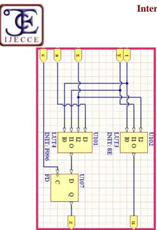
The division algorithm for 8 bit operands was implemented as a hierarchical multi-sheet schematic in “Altium Designer”: on the lowest hierarchy level is the schematic of the basic subtractor cell (Fig. 1), at the medium level is the matrix structure (an 8 x 8 extension of the Fig. 2. schematic) and at the top level is the main schematic with port connections, the operand registers and the other circuits, which form the user interface (Fig. 3).
Copyright © 2012 IJECCE, All right reserved and the solution must be given somehow empirically,
based on the designer intuition and expertise [8].
The project was tested on a “Digilent Spartan-3” development board [9], with a Xilinx XC3S200 FPGA chip. As input devices, this board has 4 push-buttons to generate user command signals and 8 bi-positional slide switches that can be used for binary number input. As output devices, the board also provides 8 binary aligned LEDs to display various signals and 4 digits of 7 segments LED-display (with decimal point), for data output.
The input numbers X, Y and the output numbers Q, R are stored in 8 bit bus version registers with clock enable, type FD8EB [7]. The output buses of the registers X and Y are connected to the matrix inputs and the results are taken from the matrix outputs to the input buses of the registers Q and R.
To view all four 8 bit numbers in a hexadecimal form on the 7 segment display, the X can be multiplexed with Q, and the Y can be multiplexed with R at the same time, by two 2 to 1 multiplexers for 8 bit buses, type M8_B2B1. The user controls what numbers are shown on the display (in the form
XXYY or QQRR digits), with the push-button PB0 that gives the selection signal XYQR for the multiplexers.
The bi-positonal slide switches connected at the input port SW[7..0] were used to insert the dividend X and the divisor Y, one after another, in 8 bit binary form. To do this, the user must first position all the switches for the X value, then press the push-button PB3 to generate LDX signal which act as “clock enable” for the X register. After that, the position of the switches must be altered again for the new value Y, and the push-button PB2 should be pressed to activate LDY signal, which is “clock enable” for the register Y. The binary form of the numbers that will be loaded can be seen in any moment on the alligned LEDs connected at the LD[7..0] output port, which reflects the state of the slide switches.
The 7 segment LED digits are used in a time-multiplexed manner, by enabling only one digit at the time to display the image placed on the SEG[7..0] common output bus. The digits must be selected cyclically, with a frequency greater than 200 Hz, to assure that no digit will be dark more than 20 ms. A scan frequency of 763 Hz was chosen for this application, by using two cascaded clock divider symbols of type CDIV256DC50 that divide the 50 MHz system clock by 2 x 256 and a duty cycle of 50 %.
The user should then press push-button PB1 to activate the DIV signal that will load the quotient Q and the remainder R registers, at next positive clock edge. Because the user can react much more slowly that any system clock, there is no need for a “ready” signal.
The 7 bit output buses from the decoders were adapted to the 8 bit input buses of the digit multiplexer DM by using special bus joiners that allow any mapping of different width bus sections. Each decimal point LED signal is extracted from its bus using a separated bus entry and all this four signals are further joined together to form a 4 bit bus connected to the push-buttons. In this way, the corresponding decimal point of each LED digit can be used as a witness for the state of one push-button.
Copyright © 2012 IJECCE, All right reserved of the display. The output busses are then inverted to
match the active low level required by the board. To avoid division by zero, a simple trick was made: a bus NOR gate detects the presence of the “zero” value in the Y register and maintains the counter C in asynchronous reset with the YEQ0 signal. The effect on the display was quite useful: the scanning is stopped and only the last digit is lighted with a “0” image on it, until a new non-zero value will be loaded into the Y register.
V. EXPERIMENTALRESULTS
The described design was implemented in a Spartan-3 XC3S200 FPGA produced by Xilinx, using the “Altium Designer” software for schematic capture and Xilinx ISE 9.2 for FPGA synthesis, translation and implementation.
The Xilinx ISE software automatically runs a timing analysis on the design, ensuring the timing constraints (like the system clock period) are met. It also reports the highest combinational path delay in the design and the highest clock frequency at which the design can run. It is so possible to extract the design performance characteristics from the timing analysis report.
The presented design was synthesized and was able to run at 13.92 MHz, having a propagation time of 71.84 ns.
To improve throughput, pipeline stages were inserted into the matrix. Taking into account the regularity of the matrix, and so the virtually equal propagation times on all lines, a pipeline register can be inserted after each line, on the z output. Also, because of the modular hierarchical design, the pipeline stage can be inserted in the matrix cell, as a D type flip-flop.
The pipelined design was synthesized and was able to run at 80 MHz. Although the pipeline latency is 8 x 12.5 ns, meaning the first result is available at the output after 100 ns, once the pipeline is full, each result is available after only 12.5 ns, which is a great improvement over the entirely combinational version.
Copyright © 2012 IJECCE, All right reserved The new resulted design was able to run at 106
MHz, with more than 20% speed improvement. In Fig. 5 is presented a screen capture of the implementation report for the pipelined version with LUT sub-tractor, as prove of the pretended results. This report was generated by the Xilinx tool “Trace” and summarized by “Altium”. All the experimental results obtained by authors are presented in Table I.
There are other papers regarding hardware implementations of division algorithms. While [11] is concerned with the effective CMOS implementation of the algorithm, [12] presents a FPGA implementation designed in VHDL. The implementation presented here is different from both and it has the portability advantage that HDL descriptions provide (because it uses generic libraries), but at the same time offers a visual description of the algorithm, through the schematic design. This paper also try to present some heuristic methods required for the implementation of user interfaces, which are applicable in other, more general implementations of the execution sections from any complex automaton [9].
VI. CONCLUSIONS
A method to implement an integer division algorithm in FPGA hardware was presented. The matrix structure from [3] was improved by eliminating unnecessary cells. This leads to a significant improvement because it optimizes the pipeline implementation, as all matrix lines have equal propagation times.
Three implementation versions were designed and compared: a fully combinational version, a generic pipelined version, and a technology specific pipelined version. Also, the design method and tools usage was emphasized, aiming to contour a design methodology for FPGA implementation of hardware algorithms.
ACKNOWLEDGMENT
This work was supported by The National Centre for Programs Management from Romania under the research grant SICONA–12100/2008.
REFERENCES
[1] C. Maxfield, FPGAs: World Class Designs, Newnes -Elsevier, 2009.
[2] K. Bhattacharyya, R. Biswas, A. S. Dhar, S. Banerjee,
“Architectural design and FPGA implementation of
radix-4 CORDIC processor”, Microprocessors and
Microsystems, Vol. 34, No. 2-4, March-June 2010. [3] J. P. Deschamps, G. J. A. Bioul, G. D. Sutter, Synthesis
of Arithmetic Circuits: FPGA, ASIC and Embedded Systems, John Wiley & Sons, 2006.
[4] Z. Navabi, Digital Design and Implementation with Field Programmable Devices, Kluwer Academic Publishers, 2005.
[5] N. Mokhoff, “NASA expands Altium tool use”, E. E.
Times, 30 October, 2007. Available: http://www.eetimes.com.
[6] A. D. Ioan, “New techniques for implementation of
hardware algorithms inside FPGA circuits”, Advances in
Electrical and Computer Engineering, Vol. 10, No. 2, 2010.
[7] User Guide, “Spartan-3 Starter Kit Board”, Digilent Inc.,
2005. Available: http://www.digilentinc.com.
[8] N. Takagi, S. Kadowaki, K. Takagi, “A hardware algorithm for integer division”, Proceedings of the 17th
IEEE Symposium on Computer Arithmetic, 2005. [9] J. Kolouch, “Combinational divider in FPGA”,
Copyright © 2012 IJECCE, All right reserved AUTHOR’SPROFILE
Eshwararao. Boddepalli