Available Online at www.ijpret.com 95
INTERNATIONAL JOURNAL OF PURE AND
APPLIED RESEARCH IN ENGINEERING AND
TECHNOLOGY
A PATH FOR HORIZING YOUR INNOVATIVE WORK
FRONT-END DESIGN FLOWS FOR SYSTEMS ON CHIP: AN EMBEDDED TUTORIAL
KAD VB, GAWADE DV
Department of Information Technology, Karmaveer Bhaurao Patil College Vashi, Navi Mumbai, India
Accepted Date: 16/08/2014; Published Date: 01/09/2014
Abstract: This tutorial describes the design flows, that is, the design steps and software tools required for designing modern systems-on-chip, focusing on the front end part. A simple flow starting with abstract design description in an HDL and going through transformations leading to physical design, is no longer adequate for the complex systems of today. A high end MPSoC (multiprocessor system on chip) today includes, apart from multiple processors, multiple memory modules, high performance interconnection network, custom hardware blocks, and a variety of controllers and interfaces. Some of the issues that need to be addressed while designing such systems are - integrated design of hardware and software, customization of processors for given applications in order to get the right power performance tradeoffs, use of certain platforms and pre-designed IPs, design of interconnection mechanisms among the processors and mapping of application onto the architecture. Therefore, our description of design flow includes several ‘sub-flows’ that are required to take care of these aspects.
Keywords: Design flow; SoC Platform; Simulation; Prototyping; Communication Architecture; ASIPs
Corresponding Author: MS. VRUSHALI BHANUDAS KAD
Access Online On:
www.ijpret.com
How to Cite This Article:
Kad VB,Gawade DV;IJPRET, 2014; Volume 3 (1): 95-108
Available Online at www.ijpret.com 96 INTRODUCTION
The sequence of steps required to accomplish the design of an integrated circuit or a systems is called Design Flow. A design flow defines not only the steps to be followed, but also the software tools required to carry out those steps. In a simple case, the design starts with some form of an abstract representation that gets progressively transformed into a manufacturable form as the designer goes through the steps prescribed in the flow. More realistically, the flow is not just a linear sequence of steps. The need to satisfy various design constraints or to get a design closure, forces the designer to iterate over several steps. This happens because while taking a design decision at an earlier stage, its impact on a later stage cannot always be accurately predicted.
Frontend Design Flow
The earlier phase of a design flow dealing with functionality and performance is referred to as the front end design flow, whereas the later phase dealing with circuit details and layout is called the back end flow. In this tutorial, we focus on the front end flow only.
Over the last three decades, as the complexity of circuits being designed has increased by several orders of magnitude, the front end design flows have seen a paradigm shift from Capture and Simulate methodology to Describe and Synthesize methodology to finally
Specify, Explore and Refine methodology [1].
The Capture and Simulate methodology was based on design entry in the form of schematic diagrams and simulation dominates the flow.
To cope up with increasing size of the circuits, there was a shift from structural design descriptions in the form of schematics to behavioral descriptions using Hardware Description Languages such as VHDL and Verilog. The most common abstraction level of design entry in Describe and Synthesize methodology has been register-transfer level (RTL). Synthesis tools are used to bridge the gap between the design abstraction levels at entry and exit points.
Available Online at www.ijpret.com 97
made. Languages such as SystemC, System Verilog, SpecC etc. are used to specify system level behavior at a comparatively higher level of abstraction.
Earlier systems on chip (SoCs) were built around a single embedded processor. Increasing demand for performance is driving the SoC architecture towards integration of more and more processors on a single chip, giving rise to Multi Processor SOCs or MPSoCs. A high end MPSoC today includes, apart from multiple processors, multiple memory modules, high performance interconnection network, custom hardware blocks to perform some critical functions, and a variety of peripheral controllers and interfaces. The processors could be standard off the shelf modules or custom designed for the given application. An MPSoC requires a design flow that is a combination of several sub-flows, each taking care of a different requirement.
SoC Platforms and IPs
As design entry moves towards higher levels of abstraction, the basic building blocks evolve towards more complex components such as processors, on-chip memory, and custom designed cores. Design reuse oriented paradigms drive the integration of such third-party intellectual property (IP) cores into Systems on chip; such cores would be pre-verified and lead to a tremendous productivity boost and reduced design times. The designer may still include custom-designed and synthesized functional blocks as a differentiating factor. However, the overall design methodology needs to be aware of the requirement that much of the SoC will consist of instantiations of reused blocks. The hardware and software architecture and interfaces of the SoC need to be appropriately designed in order to enable a clean composition of design elements that may have their origin in disparate vendors and design groups.
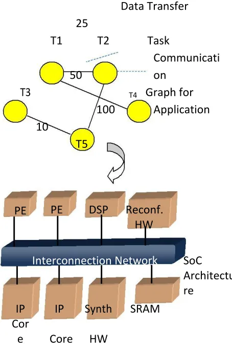
SoC Architecture and Task Mapping/ Scheduling
Available Online at www.ijpret.com 98
In addition to the processor core, the SoC architecture platform may consist of several types of memory cores including instruction and data caches, SRAM cores serving as scratch pad memory, and FIFO structures. The personalization of such modules is usually performed through a memory-compiler tool that can generate the layout of the required configuration.
Programmable components present in modern SoC fabrics may also include some reconfigurable logic of the type present in FPGAs (Figure 1). This allows for minor updates to the hardware functionality post-deployment as well as for future versions of the SoC.
Finally, the architecture platform may accommodate custom hardware designed with a traditional HDL synthesis and physical design flow. Appropriate interfaces need to be implemented for such hardware to communicate with other IP blocks.
Available Online at www.ijpret.com 99
Figure 1 Application Mapping to SoC
Commercial tools such as CoWare’s Platform Architect [3] offer graphical capture tools for building and customizing system level platforms.
Concurrent Software Development
To cut on the development time, software development needs to be carried out concurrently while the hardware architecture is being explored. This can be done using a simulated model of the architecture. Different simulation models are required at different stages. Requirements of software developers are different from those of system architects and hardware implementers. Hardware designers need to simulate precise timings in the design to verify its behavior. System architects also need timing information, though not very precise, for design space exploration and selection of suitable architecture. In contrast, software developers need only functionality
25
Data Transfer
T1 T2 Task
50
Communicati on
T3
100
T4 Graph for
10
Application
T5
PE PE DSP Reconf.
HW
Interconnection Network SoC
Architectu re
IP IP Synth SRAM
Cor
Available Online at www.ijpret.com 100
of the hardware to be simulated, ignoring the timing details. However, they require a faster speed of simulation since the software running over simulated hardware adds a layer of interpretation.
Since timing details are not relevant at this stage, simulation speed can be increased by excluding these details from the simulation models, thus raising the level of abstraction. This means that while functionality of the instructions is modeled, the micro-architectural and cycle level details are omitted. Based on this principle, Virtual Prototyping Environments (VPEs) are created to facilitate software development concurrent with hardware development.
VPEs include high level executable models of various subsystems such as processors, memories, peripheral controllers, interconnecting buses, networks, etc. The processors are modeled using instruction set simulators (ISS), enclosed in appropriate wrappers to communicate with other subsystems. The communication among the subsystems is also modeled at an abstract level such as TLM (Transaction Level Modeling [4]).
Communication Architecture
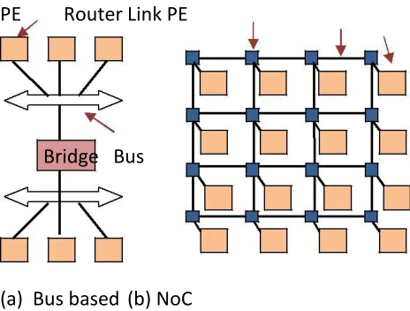
When an SoC is composed of blocks of hardware sourced from different design groups or companies, there is a fundamental need to define and strictly adhere to appropriate communication architecture and protocols to be used for inter-core communication. On -chip communication architectures have traditionally been bus-based, with recent years witnessing a surge of interest in packet -switched Network on Chip (NoC) architectures. Figure 2 shows these two alternatives.
Bus Based
Available Online at www.ijpret.com 101
Bus widths here are smaller and the simpler protocol such as non-pipelined transactions enables power saving.
PE Router Link PE
Bridge Bus
(a) Bus based (b) NoC
Figure 2 Communication Architecture Topology
When bus based architecture is selected for an SoC, several important system-level decisions still need to be taken. These relate to architectural parameters necessary to complete the instantiation of the bus, such as:
• Bus width,
• Clock frequency,
• Topology and partitioning into smaller hierarchical units, and
• Choice of arbitration scheme.
The solution to the above problem of suitable choice of bus parameters can involve quite intricate analysis and optimal solutions may be hard to obtain. To arrive at the right topology, we would need to first represent the communication requirements between tasks mapped to different processing units connected to the bus. A heuristic bus topology generation strategy can assign processing elements executing tasks to a bus if sufficient capacity is estimated to exist. If the capacity is insufficient, then a new physical bus instantiation may be made. In general, a trade-off would exist between the cost of a selected bus topology and the resulting performance.
Networks on Chip
Available Online at www.ijpret.com 102
structures present performance bottlenecks since the resulting latencies and throughput may be unacceptable. NoCs, which rely on packet switching mechanisms, borrow heavily from traditional concepts used in computer networking, and are applied to systems on chip. As usual, such remapping of useful concepts to the on-chip domain results in obvious well-known benefits, while at the same time opening up new challenges and research opportunities. While the ideas of networking are reused, the customization of these architectures for SoCs throws up some novel research problems and solutions.
An NoC consists of the standard network components:
(1) a set of processing elements (PE); (2) a set of routers for managing the flow of traffic to and from the PEs; (3) a network interface connecting each PE to a router, and (4) a set of links connecting the routers into an on-chip network. The router is a fundamental unit in NoC architectures and considerable attention has been focused on its design. A generic router may be viewed as consisting of the following components:
• Input and output ports: a router has several ports, and through these, is connected to a
local PE and a subset of the other routers in the network.
• Buffers attached to ports in the routers can store packet data in transit
• Routing logic, consisting of some arbitration mechanisms, is responsible for maintaining the
flow of control at the routers
• A basic switching fabric enables the transfer of data between ports of the router.
Data packets are organized into several flits (flow control units), and routers are usually capable of buffering flits at their input and output ports. Grid or mesh structures are commonly employed as typical interconnection topologies for NoC routers because of their scalability and geometric regularity.
Available Online at www.ijpret.com 103
disturb the advantages of regularity is to superpose a few long-range links in a regular topology; this improves performance while affecting other properties minimally.
As researchers continue to explore different aspects of NoC architectures and their customization strategies, important questions still need to be answered regarding the advantages of NoC over bus-based architectures. While NoCs certainly address some of the scalability problems of bus based communication architectures and deliver higher throughput, they carry a significant cost overhead in terms of area and power, which may render them unsuitable in many applications that operate under such constraints. Researchers are investigating hybrid communication architectures that employ simple buses for local clusters of cores, but switch to routers and networks for long-distance traffic across clusters.
Customizing Processor Architectures
Need for Customized Processors
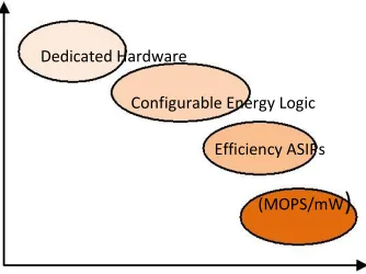
Off the shelf processor cores are often unable to meet stringent performance / energy constraints that some applications may have. Implementing these as dedicated hardware blocks leads to very inflexible solutions. In such cases, a custom designed or Application Specific processor can potentially offer the right combination of flexibility and performance / energy. As shown in Figure 3, an Application Specific Instruction Set Processor (ASIP) can be nearly as flexible as a standard (off the shelf) processor while competing fairly well with an ASIC or dedicated hardware.
Dedicated Hardware
Configurable Energy Logic
Efficiency ASIPs
(MOPS/mW)
Standard Processors
Flexibility
Available Online at www.ijpret.com 104 Architecture Space
There are two broad approaches for designing application specific processor architectures.
1. Start with base processor architecture and identify changes in it to suit the given application
[6].
2. Define a new architecture, starting from scratch, for example [7].
The first approach allows limited variations in the processor architecture but makes it easier to arrive at a solution. For example, Tensilica provides a base architecture called Xtensa LX2 [8] shown in Figure 4. Methods to customize this architecture include configuring certain parameters (e.g. register file size) or optionally including certain modules such as multiply-accumulate unit, audio engine, memory management unit etc., or adding user defined extensions such as execution units and register files.
Base ISA features Configurable
Function
Instruction fetch decode
FLIX pipelines Base pipeline
Execution units, Register file Memory
Designer RFs and
ALU
interfaces
defined interfaces
extensions MAC16/32
FPU Zero o/h loop
DSP Audio engine Trace and
User defined debug
EUs
Interrupt control, Timers
Optional functions Optional and configurable
Figure 4 Tensilica’s Xtensa LX2 Architecture
Available Online at www.ijpret.com 105
versatile Architectural Description Language (ADL) to specify the new custom architecture in its totality. Examples of ADLs include EXPRESSIONS [7], MDES [9], LISA [10].
Tool Chain for Customized Processors
Once a custom processor is defined, several tools are required in order to use it. First of all, a compiler-assembler-linker chain is required to generate code for the given application. Secondly, a simulator is required to execute the application code. This is usually an instruction set level simulator (ISS) wrapped in a system description language such as System C to be plugged in a VPE (see section 5). Thirdly, an RTL description of the processor is required to be produced which can be used for synthesizing processor hardware. An alternative to generating new tools for a given architecture is to have generic tools which accept the description of processor architecture as an input. For example, a retarget able compiler which can generate code for the specified processor architecture can serve the purpose. Designing such generic tools is certainly a hard task.
Architecture Exploration
The design space of processor architectures can be explored for a given application using compiler and simulator. This is usually done in ADL based approach. Figure 5 shows the design flow with LISA Tek tools from Co Ware following this approach [11]. The designer may use the architecture samples available in a library as a starting point. The processor designer tool generates the software tools that are used for compiling the application and simulating it over the specified architecture. If required, the architecture description is modified and the process is repeated.
Application C/C++
LISATek Software
Architecture Custom processor Tool
samples processor designer Chain
model in LISA 2.0
Analyze and debug
SoC S/W RTL
Integration dev (SystemC) tools
Available Online at www.ijpret.com 106
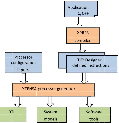
The approach involving extension of a base processor lends itself to some degree of automated design space exploration. In particular, techniques for automated identification of application specific instructions and design of customized functional units to implement these instructions have been well researched. As an example, application analysis and custom instruction set identification using Tensilica’s XPRES tools [12] is shown in Figure 6.
Here the XPRES compiler analyzes the application program to identify computational patterns which may be included as new instructions. Customized functional units to implement these instructions are also added to the architecture. The system accepts manually defined configurations, options and extensions, as well as automatically identified extensions, expressed in a language called TIE. From the specifications, the processor generator produces the software tool chain.
EMULATION / PROTOTYPING
Simulation is extensively used for verifying and analyzing the designs at various stages in the design flow. Thus a significant amount of designers’ time is actually spent in simulation activity. The simulation time grows rapidly with circuit size. Therefore, speed of simulation is very important for SoC design teams. Thus, a lot of attention has been paid by the EDA community on speeding up the simulation process. A technique to speed up simulation by a significant amount involves using hardware to execute the simulation models.
Execution of models in hardware is called emulation. The standard off the shelf modules of the system can be emulated by fixed hardware elements, whereas, programmable / configurable hardware such as FPGAs can be used to emulate standard as well as custom designed modules. Availability of high capacity FPGAs has made it possible to have hardware models of fairly large systems, running 2 – 3 orders of magnitude faster than software simulators. Examples of major commercial products for emulation are Palladium from Cadence [13] and Veloce from Mentor Graphics [14]. These systems can be used in two modes.
1. Only the critical part of the design being simulated is mapped onto the emulation system
while the remaining part continues to be simulated in software. The overall control remains with the software and the same test bench is used. Appropriate interfaces on software and hardware side are required to seamlessly move a part of the design to the emulator. This approach is known as simulation acceleration or hardware assisted simulation.
2. Depending upon the size, the entire design may be mapped to the emulation system and run
Available Online at www.ijpret.com 107
A process similar to emulation is prototyping. Here a design closer to its final implementation is mapped to configurable hardware. This may not have extensive debug environment like that of simulators or emulators, but it allows the design to be tested in a more realistic setting.
Application
C/C++
XPRES
compiler
Processor
TIE: Designer configuration
defined instructions inputs
XTENSA processor generator
RTL System Software
models tools
Figure 6 Automatic Instruction Generations by XPRES Compiler of Tensilica SUMMARY
Design of an SoC for a given application or application domain is a very complex task. In this tutorial we have discussed the initial phase or the front end flow of this task. The main steps discussed were platform and IP integration, application to architecture mapping, concurrent software development and exploration of communication architecture, processor customization and emulation/prototyping.
REFERENCES
1. D. D. Gajski, F. Vahid, S. Narayan, and J. Gong, SpecSyn: An Environment Supporting the
Specify-Explore-Refine Paradigm for Hardware/Software System Design, IEEE Trans. on VLSI Systems, 6(1), pp. 84-100, March 1998.
2. R. Marculescu, U. Y.Ogras, L.-S. Peh, N. E. Jerger, and Y. Hoskote, Outstanding Research
Available Online at www.ijpret.com 108
3. http://www.coware.com/products/platformarchitect.php
4. http://www.systemc.org/
5. ARM AMBA Specification and Multi-layer AHB Specification (rev2.0), http://www.arm.com,
2001
6. C. Galuzzi and K. Bertels, The Instruction-Set Extension Problem: A Survey, Proc.
International Workshop on Applied Reconfigurable Computing 2008, R. Woods et al. (Eds.) LNCS 4943, pp. 209–220, Springer-Verlag 2008.
7. P. Mishra, A. Shrivastava and N. Dutt, Architecture Description Language (ADL)-Driven
Software Toolkit Generation for Architectural Exploration of Programmable SOCs ACM TODAES, 11(3), July 2006, pp. 626–658.
8. http://www.tensilica.com/products/xtensa-customizable/xtensa-lx2/architecture-2/
9. The MDES User Manual, http://www.trimaran.org/docs/ mdes_manual.pdf
10.O. Schlie busch, A. Hoffmann, A. Nohl, G. Braun and H. Meyr, Architecture Implementation
Using the Machine Description Language LISA, ASPDAC, pp. 239-244, 2002.
11.http://www.coware.com/products/processordesigner.php
12.
http://www.tensilica.com/products/hw-sw-dev-tools/for-processor-designers/xpres-compiler.htm
13.http://www.cadence.com/products/sd/palladium_series