Vol. 47, No. 1, Spring 2015, pp. 23- 29 )AIJ-EEE)
٭
Corresponding Author, Email:[email protected]
Design and Simulation of a Modified 32-bit ROM-based
Direct Digital Frequency Synthesizer on FPGA
P. Soleimani Abhari
1and M. Dosaranian Moghadam
2٭1-MSc. Student, Department of Electrical, Biomedical and Mechatronics Engineering, Qazvin Branch, Islamic Azad University, Qazvin, Iran
2-Assistant Professor, Department of Electrical, Biomedical and Mechatronics Engineering, Qazvin Branch, Islamic Azad University, Qazvin, Iran
ABSTRACT
This paper presents a modified 32-bit ROM-based Direct Digital Frequency Synthesizer (DDFS).
Maximum output frequency of the DDFS is limited by the structure of the accumulator used in the DDFS
architecture. The hierarchical pipeline accumulator (HPA) presented in this paper has less propagation delay
time rather than the conventional structures. Therefore, it results in both higher maximum operating
frequency and higher maximum output frequency. Ripple Carry Adder (RCA) is used at each stage of
Conventional pipeline accumulators, whereas the modified pipeline technique contains Carry Look-ahead
Adder (CLA) instead of RCA. The proposed method consists of hierarchical adders that have three parts, two
blocks of 4-bit CLA and a separated block to estimate carry bits independently. To reach a better frequency
resolution in the DDFS, larger phase accumulator is needed. Moreover, in conventional DDFSs, as the
number of phase bits increases, to have non-truncated phase mapping, huge amount of memory will be
needed. The trigonometric relations of the sine and the cosine functions are used in the phase mapping
technique proposed by Symon in order to reduce the size of the Look Up Table (LUT). The method applied
in this work combines quarter wave symmetry of the sine samples, the phase difference between the sine and
the cosine samples and trigonometric relations of the sine and the cosine functions to reduce the total
memory size. The SFDR of the output wave will remain approximately constant (132 dBc) in comparison
with the previous works. Finally, the proposed architecture is simulated on Stratix II FPGA. This structure
has the frequency range of 0 to 245 MHz with 0.05 Hertz frequency resolution.
KEYWORDS
1- INTRODUCTION
The most common method of generating analog signals by digital operations is Direct Digital Frequency Synthesizer (DDFS) that is mostly concerned with sinusoidal waveforms. The DDFS has many advantages in comparison with other methods like micro Hz frequency resolution, including fast hopping, remote controlling ability, and wide frequency range. In addition, its architecture can be changed by software. Conventional DDFSs consist of three main parts. The first part is the phase accumulator (PA) that produces phase values with an adjustable step called Frequency Control Word (FCW). The second part is the Look Up Table (LUT) that is usually a ROM to store the sine and the cosine samples at different phases and maps input phase value to its corresponding amplitude. Finally, the digital to analog convertor is the third part of conventional DDFSs that results in analog output wave. A low pass filter can be used to eliminate unwanted harmonics (see figure 1). Output frequency of the DDFS depends on FCW, fs (system clock) and the size of the
phase accumulator (N) by the following equation:
fout=FCW*fs/2N (1)
The frequency resolution of the output wave will be clearly attained by choosing FCW=1, so the resolution is reached by fs/2N. It is deduced that the maximum output
frequency and the frequency resolution have direct relation with the clock frequency. Most significant part of the DDFS that affects operating frequency is the PA. To reach higher operating frequency, several structures have already been presented like pipelining techniques [1]. Using CLA adders instead of RCAs could result in better performance in pipeline architectures [2]. There is an architecture known as parallel pipelined accumulator in the literates [3]. This architecture combines paralleling and pipelining techniques. These structures can improve the maximum operating frequency. Disadvantages of these structures include having long latency time and so many amount of registers consumption as delay elements, especially when the size of the accumulator is large. The number of adders used in this structure increases by factor of four rather than PAs. This paper presents a high speed 32-bit hierarchical pipeline accumulator that consists of 8-bit hierarchical carry look-ahead adder (HCLA) at each pipeline stage. The proposed PA could improve the maximum output frequency. Large accumulator will be needed in order to reach the acceptable frequency resolution that increases the size of the accumulator feeds the LUT, so it will cause huge amount ofmemory consumption due to their exponential relation. Assume that N-bit phase accumulator will generate phase values from 0 to 2N-1, the phase sequence Φ(n) is generated by the accumulator clocked at the sample rate fs, and the phase increment value FCW is
reached by Φ(n)=mod (n*FCW,2N), the phase initial
value is considered zero for simplicity. A ROM (LUT) with 2N address line is needed to store these phase
corresponding amplitudes so that ith location of the LUT stores sin(2π*i/2N) values and the phase mapped signal is
sin(2π*n*FCW/2N). Phase truncation is a common
method to reduce the total memory consumption. In this method, less significant bits of the phase value are ignored and remaining MSBs are used for addressing the ROM. Suppose I bits of the N bits phase number are used for addressing and F bits are eliminated, the ROM size is reduced to 2I. In this approach, the frequency resolution is remained constant but an error called phase truncation error (ε(n)) that causes spurious components in the frequency domain appears as Eq.(2) and the Spurious Free Dynamic Range (SFDR) is affected as Eq.(3) [4]. ε(n)= Φ(n)-2F[Φ(n)/2F] (2)
SFDR=6.02*I (3) There is a trigonometric ROM compression method that could reduce the total memory size by factor of 534.2:1, but in this work, phase truncation is used and the SFDR is not studied [5]. Phase dithering is a common method that can be used to improve the SFDR that is affected by phase truncation. Guoping Wang improves the SFDR of the standard DDFS from 45 to 65 dBc using this method [6]. In addition, the CORDIC algorithm is one of the phases to amplitude conversion methods by applying coordinate rotation algorithm. In this way, the sine or the cosine of an angle can be calculated [7]. Another phase mapping technique is presented by Symon that reduces LUT storage memory without phase truncation [8]. This method is modified in this paper using quarter wave symmetry and the phase difference between the sine and the cosine samples. The fine and the coarse LUTs size can be reduced by introducing another work called Symon’s modified method [9].
The rest of this paper is organized as follows. In Section II, architecture of the phase accumulator is discussed and types of the adders and their affect on the maximum frequency of the accumulator is studied. In this section, the hierarchical carry look-ahead adder is also introduced. Section III concerns phase mapping techniques, especially phase mapping by trigonometric identities and optimization of the ROMs used in the phase mapping method. In Section IV, the proposed DDFS are presented. In addition, the novel phase accumulator and the modified method of phase mapping are covered in this section. Simulation results and comparisons are
demonstrated in Section V, and finally the conclusions are presented in Section VI.
2. THE PHASE ACCUMULATOR
ARCHITECTURE
2.1. PIPELINE ACCUMULATORS
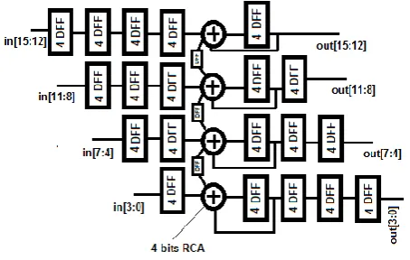
In the pipeline architectures, an N-bits accumulator is divided into M stages, each of them consists of L-bits RCA or CLA so that M*L=N. Each stage takes input and gives output independently. Indeed, the input word is divided into M words that feed each stage separately. Output carry bit of each stage is transferred to higher stage through an interface register as delay element that is used to balance time interval the input carry and input reach the adder. Figure 2 is the schematic of 4-stage 16-bit pipeline accumulator that uses RCA as adder. Using 4-bit CLA instead of RCA could reach 10.5 percent higher maximum frequency in the 16-bit pipeline architecture [2].
Fig. 2. The 16-bit pipeline accumulator [2]
2.2. HIERARCHICAL CARRY LOOK-AHEAD
ADDER
The types of the adders are used in the pipeline structure is the most significant factor in order to achieve maximum operating frequency. In this work, the applied standard size of the adder in pipeline stages is 8 bits. 8-bit RCA needs 8 times carry rippling from position 0 to7 that limits the maximum operating frequency due to the long propagation delay time. Likewise, 8-bit CLA uses complex calculations to determine output carry, that takes more delay time and power consumption. There are several methods to reduce complexity, power consumption and delay time in CLAs, hence, the most common method is dividing the 8-bit CLA into two 4-bit parts in cascade form. As a result, carry bits of each part is calculated separately and output carry of part 1 is transferred as input carry of part 2. Carry rippling between two separated blocks in cascade CLA takes propagation delay time that limits the operating frequency. The Hierarchical Carry Look-ahead Adder (HCLA) is used in this work to reach higher operating frequency [10]. To do so, 8-bit CLA is divided into two 4-bit CLA in cascade form, then two parameters as group propagation P0-3 and group generation G0-3 are defined
and a separate block is used to estimate if the 4-bit CLA will generate or propagate carry bit or not. The separate block for carry estimation that is called look-ahead block computes carry bits independently through the following rules. The 4-bit CLA will have output carry when: position 3 generates a carry or position 2 generates and position 3 propagates it or if position 1 generates and position 2 and 3 propagate or finally if position 0 generates and others propagate, clearly the equation of the group generation is as follows:
G0-3=G3+G2P3+G1P2P3+G0P1P2P3 (4)
Likewise, the 4-bit CLA block will propagate input carry when all positions propagate it and the propagation equation is defined as:
P0-3=P0P1P2P3 (5)
Figure 3 shows the block diagram of the 8-bit HCLA. In Table 1, the simulation results of the combinational logic circuit on Cyclone II device show that 8-bit HCLA has less propagation delay time in comparison with 8-bit CLA and 8-bit RCA under the same conditions.
TABLE 1. COMPARISON OF MAX tpd OF VARIOUS
ADDERS
Adder type Max propagation delay (tpd)
8-bit RCA 8.055 ns
8-bit CLA 7.999 ns
8-bit HCLA 7.500 ns
Fig. 3. Block diagram of the 8-bit HCLA
3. PHASE MAPPING TECHNIQUE
3.1. PHASE MAPPING USING TRIGONOMETRIC IDENTITIES
The phase truncation causes the phase number to separate into two parts. One part is an integer (I) and another is a fraction (F), so that N=I+F. Defining two phase sequences ΦI(n) and ΦF(n) as integer and fraction
and b=2*π*ΦF(n)/2N, the optional phase mapping can be
done.
ΦI(n)=[Φ(n)/2F ΦI(n) [0:2I-1] (6)
ΦF(n)=Φ(n)-ΦI(n)*2F ΦF(n) [0:2F-1] (7)
Sin(a+b)=sina.cosb+sinb.cosa (8)
Cos(a+b)=cosa.cosb-sina.sinb (9)
2πΦ(n)/2N=2π*2F[Φ(n)/2F]/2N (10)
+2π(Φ(n)-2F[Φ(n)/2F])/2N 2πΦ(n)/2N=2πΦ I(n)/2 I + 2πΦF(n)/2 N In this case, to calculate the amplitude of a phase value four LUTs is needed, each of them should be defined as T1 to T4 like the following. T1[a]=cos(2πa/2I) T2[a]=sin(2πa/2I) (11)
T3[a]=cos(2πa/2M) T4[a]=sin(2πa/2M) where T1 and T2 is called coarse LUTs and have 2I locations and T3 and T4 is called fine LUTs that have 2N locations. In Eq. 11, (a) represents the LUT’s address and Tn[a] denotes a’th location of the n’th LUT. In this technique, the maximum memory saving is attained by choosing F=I=N/2. Applying this phase mapping technique results in memory reduction by factor of 2(2-N/2) in comparison with non-truncated common method. Figure 4 shows the block diagram of the above mentioned DDFS structure. This architecture consists of four multipliers and two adders [8]. Fig. 4. Trigonometric phase mapping schematic [8] 3.2. COARSE LUT OPTIMIZATION To underestimate the memory size, the sine and the cosine quarter wave symmetry can be applied [9]. In this case, by choosing I=N/2+1 and F=N/2-1, the quarter of the sine and the cosine samples should just be stored in the coarse LUTs. Two MSBs of ΦI(n) are used to determine which cycle should be generated and remaining MSBs are used for addressing. Assume that the first quarter cycle of the sine samples is stored in the sine coarse LUT. First, both MSBs of ΦI(n) are zero and both the phase values feed the LUT and output of the LUT will not change. At the second quarter cycle, second MSB equals one and first MSB is zero, therefore, in this case, the LUT should be swept from the last address to the first. Thus, the address line should be complemented but the output will not change and so on. Figure 5 shows the coarse LUTs applying quarter wave symmetry for the coarse LUTs. Fig.5. The LUTs optimization using quarter wave symmetry 3.3. FINE LUT OPTIMIZATION The sine fine LUT contains the sine values at the phases between 0 to (2π*2N/2-1/2N) angles due to the Φ F(n) interval, that are very small, as a result , the first bits of the stored values can be ignored. For the cosine fine LUT, the values of cosine function are near 1, so the above-mentioned strategy is not remedial. For this reason, values of 1-cos(ΦF(n)) can be replaced and the phrase cosa.cosb in Eq. (9) can be substituted as Eq.(12) [9]. cosa.cosb=cosa-(1-cosb)cosa (12)
4. PROPOSED DIRECT DIGITAL FREQUENCY
SYNTHESIZER
4.1. PROPOSED PHASE ACCUMULATOR
(HPA)
MHz in 16-bit structure, although the total memory bit is remained constant, but HPA has more logic elements. The results can be extended for 32-bit structures.
Fig. 6. Block diagram of the 32-bit HPA
4.2. PROPOSED PHASE MAPPING
TECHNIQUE
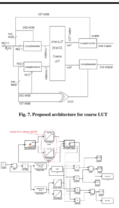
Surely, there is π/2 phase difference between the sine and the cosine functions, noting the fact that just one coarse LUT is needed in the trigonometric phase mapping technique to generate both the sine and the cosine coarse values. In this research, a ROM with two address lines and two outputs is used. In the proposed structure, finally, the values of the sine function between 0 to π/2 are stored in the coarse LUT. The N- bit phase value is separated to N/2+1 bits as integer part and N/2-1 bits as fraction part, so those two MSB bits of the integer part of the phase are used as enabled bits of the complementers to regulate the address lines and the outputs of the ROM corresponding to the each cycle, as figure 7 illustrates. For instance, the address line 1 at the first quarter cycle will be remained unchanged because the first quarter cycle of the sine samples is stored but the address line 2 will be complemented because of π/2 phase difference between the sine and the cosine samples. Address line 1’s complement is used in this work for complementing that can be implemented simply using XOR. Of course, ½ LSB (1/2 of phase accuracy) phase shift should be applied for the sine samples because otherwise 0 and π/2 will have the same address when using 1’s complement that causes an error to affect the SFDR. To produce errorless minus half cycle, -1/2 LSB offset is included for amplitude values. Similarly, fine LUT optimization method is used and the size of the each fine memory location can be reduced from 22 bits to 14 bits without affecting the SFDR. Figure 7 illustrates the main structure (coarse part) of the proposed method and Figure 8 shows the proposed architecture block diagram that is simulated by Simulink Matlab.
5. SIMULATION RESULTS
Noting the simulation of the proposed 32-bit HPA and conventional methods on Stratix II device, the proposed HPA could reach higher operating frequency, but total
logic elements used in the design have been increased. The maximum operating frequency of the 32-bit HPA is 273 MHz that is approximately 40 MHz more than conventional PA. Table 2 represents the simulation results and the comparison among other structures. Likewise, various types of the phase to amplitude conversions (16-bit architectures) are simulated by Matlab Simulink and the SFDR of the output waves and the memory consumption are compared as Table 3 shows. The simulation proves that the SFDR of the output wave is remained constant, although the total storage memory is reduced by eliminating one coarse LUT and applying Fine LUT optimization. Finally, the comparison results are extended to the 32-bit structure and the DDFS uses the 32-bit HPA and the proposed phase mapping technique is simulated on Stratix II FPGA. Figure 9 shows frequency domain spectrum of the output wave in the proposed architecture. The SFDR of the output wave is 132 dBc. Table 4 gives the simulation summary.
By extension of the result to 32-bit structure, it is clear that the total memory consumption is (1*2^15*22) +2*(2^15*14). In other words, a ROM with the size of 2^15*22 is eliminated and locations of two ROMs with 2^15 address lines shrink from 22 bits to 14 bits in
Fig. 7. Proposed architecture for coarse LUT
comparison with Symon’s method. In addition, Table 4 shows 28% of total memory bits of the device that are used in this architecture.
Fig. 9. Frequency domain spectrum of the output wave
TABLE 2. SIMULATION RESULTS OF THE ACCUMULATORS
Accumulator type HPA 32bits (proposed)
PA 32bits (CLA)
PA 32bits (RCA)
f max (MHz) 273.15 204.5 230
Total logic eleents 164 123 107
Total combinational
function 131 87 72
Dedicated logic
register 88 88 88
Total register 88 88 88
Total memory bits 64 64 65
TABLE 3. COMPARISON RESULTS OF THE 16-BIT DDFSS
Output wave SFDR
(dBc) Number of ROM*(ROM
size) ROM based
DDFS type (16 bits)
153 1*(2^16 *22)
Simple LUT
153 1*(2^14*22)
Quarter wave symmetry LUT
138 2*(2^8*22)+2*(2^8*22)
Symon’s method [8]
136 2*(2^7*22)+2*(2^7*22)
Modified symon’s method [9]
136 1*(2^7*22)+2*(2^7*22)
Proposed method
131 1*(2^7*22)+2*(2^7*14)
Proposed method with fine LUT
optimized
TABLE 4. SIMULATION SUMMARY OF THE PROPOSED 32-BITS DDFS ON STRATIX II
Device EP2S90F1020C3
Logic utilization < 1%
Combinational ALUTs 321/72768 (< 1%)
Dedicated logic registers 113/72768 (< 1%)
Total registers 113
Total pins 92/759 (12 %)
Total virtual pins 0
Total block memory bits 1245184/4520488 (28 %)
DSP block 9-bit elements 16/384 (4 %)
Total PLLs 0
Total DLLs 0
6. CONCLUSIONS
This paper presents a modified DDFS using trigonometric identity that uses one ROM with two address lines as the coarse LUT. Due to this fact, one coarse storage memory (2^15*22 bits) is omitted and each location of the fine LUTs (2^15 locations) shrinks from 22 bits to 14 bits using the fine LUT optimization. The SFDR of the output wave is remained approximately constant (132 dBc). Maximum operating frequency is one of the key parameters of the DDFS, so as the comparison table shows; the proposed method could improve this result approximately 40 MHz versus the consumption of more logic elements. The proposed DDFS that uses the high speed 32-bit HPA and the modified trigonometric phase mapping technique were simulated on stratix II device. This design can work with the maximum operating frequency of 245 MHz, and the frequency resolution of 0.05 Hz. The proposed structure consumes 28% of total memory bits of the device and the exact number of total registers included in this architecture equals 113.
REFFERENCES
[1] Ibrahim, S. H., Ali, S. H. M., and Islam, M. S., “Design A 24-Bits Pipeline Phase Accumulator For Direct Digital Frequency Synthesizer”, IEEE 2012 international symposium on instrumentation and measurement sensor network and automation (IMSNA), pp. 393-397, 2012.
[3] Chappell, M. and McEwan, A., “A Low Power High Speed Accumulator for DDFS Applications”, IEEE Proceedings of the 2004 International Symposium on Circuits and Systems, vol.2, pp. 797-800, May 2004. [4] Vankka, J., “Direct Digital Synthesizers: Theory,
Design and Applications”, Helsinki University of Technology Department of Electrical and Communications Engineering Electronic Circuit Design Laboratory, PHD thesis, November 2000. [5] Alkurwy, S. H., Md Ali, S. H., and Shabiul Islam,
Md., “Implementation of Low Power Compressed ROM for Direct Digital Frequency Synthesizer”, IEEE international conference on system science and engineering (ICSSE), pp. 309-312, 2014.
[6] Wang, G., “An FPGA-based Spur-Reduced Numerically Controlled Oscillator”, IEEE international conference on system science and engineering (ICSSE), pp. 187-192, 2012.
[7] Ko, Lu-Ting, Chen, Jwu-E., Shieh, Yaw-Shih, Hsin, Hsi-Chin, and Sung, Tze-Yun, “Difference Equation-Based Digital Frequency Synthesizer”, Mathematical Problems in Engineering, Hindawi, vol. 2012, pp. 1-12, 2012.
[8] Symons, P.R., “DDFS Phase Mapping Technique”, IET, Electronics Letters, vol. 38, no. 21, pp.1291-1292, 2002.
[9] Cardarilli, G.C., D’Alessio, M., Di Nunzio, L., Fazzolari, R., Murgia, D., and Re, M., “FPGA implementation of a low-area/high-SFDR DDFS architecture”, 10th International Symposium on Signals, Circuits and Systems (ISSCS), pp. 1-4, July 2011. [10] Compton, K., “Carry Lookahead Adders”, Logic and
![Fig. 1. Block diagram of the standard DDFS [4]](https://thumb-us.123doks.com/thumbv2/123dok_us/17660.2001802/2.595.313.547.77.191/fig-block-diagram-standard-ddfs.webp)
![Figure 4 shows the block diagram of the above mentioned DDFS structure. This architecture consists of four multipliers and two adders [8]](https://thumb-us.123doks.com/thumbv2/123dok_us/17660.2001802/4.595.59.287.510.686/figure-diagram-mentioned-structure-architecture-consists-multipliers-adders.webp)