Copyright © 2015 IJECCE, All right reserved
Design and Implementation of CSR for DDR4 Memory
Controller
Mr. Sathish D.
IV Sem M.Tech., Dept. of ECEBNMIT, Bengaluru, India. Email: [email protected]
Dr. PA Vijaya
Professor, Dept. of ECE BNMIT, Bengaluru, India Email: [email protected]Mr. Ramudu B
Senior Technical Architect, Graphene Semiconductor ServicesPvt. Ltd., Bengaluru, India.
Abstract – This paper deals with the design and
implementation of Control Status Register (CSR) for DDR4 memory controller and also presents proposed architecture of the DDR4 memory controller along with brief details of individual blocks. Control register stores different timing parameters to generate different timing delays for various commands for DDR4 memory like refresh, self refresh, power down entry and exit, read and write operations, On-Die Termination, different modes of operation and also updates the status register when read from or written into registers. The timing parameters are written by the APB (Advanced Peripheral Bus) master and CSR receives this information through APB slave interface which is at the controller side and stores this information in respective registers of CSR. DDR4 core part of memory controller has timing and command generator unit which reads the timing parameters from the CSR and generates timing delays for each memory related commands for DDR4 memory for proper operation and also updates Status Register on each read or write success/failure.
The entire design was coded in System Verilog hardware description language and simulated using ModelSim 10.1C version. The results of various operations were verified using different test cases.
Keywords – Memory Controller, CSR, DDR4, Digital
Circuits, APB Protocol, SDRAM.
I.
I
NTRODUCTIONEmbedded systems usually have limited amount of memory available that is because of cost, size, power and other constraints imposed by the overall system requirements. Sometimes device may have multiple masters and share common memory for their application. To increase the speed of memory operation in real time applications DDR4 SDRAM (Double Data Rate 4th Generation Synchronous Random Access Memory) memory was designed. DDR4 is a double data rate memory succeeding DDR3 announced and standardized by JEDEC (Joint Electronic Device Engineering Council); consume low power, higher densities, more banks, with a high bandwidth interface and higher data range of data transfer rates [1]. DDR4 operate at a voltage of 1.2v with frequency between 1600 and 3200 MHz compared to frequency between 800 to 2400 MHz and voltage requirement of 1.5v or 1.65v of DDR3 memory. The JEDEC standard for DDR4 SDRAM defines densities ranging from 2–16 GB. The JEDEC DDR4 standard defines clock rates up to 1600 MHz, with data rates up to 3200 Mbps [1].
DDR4 SDRAM has 8n pre-fetch architecture along with the parallel bank for the higher data transfer rate. DDR4
memory is internally configured as 16 banks, 4 bank group with 4 banks for each bank group. Some of the new features introduced in the DDR4 memory are CRC (Cyclic Redundancy Code), FGREF (Fine Granularity Refresh), temperature controlled refresh, new ODT (On Die Termination) control, CAL (Command Address Latency), Boundary scan, CA parity, Command encoding, MPR (Multi Purpose Register), DBI (Data Bus Inversion) [2].
Memory controller is a digital logic controls the data flow between the memory and processors. Consider SOC (System on Chip) and embedded products; two or more processors share the same memory for their applications on a single chip. When different processors request for the memory access, memory controller processes the received request based on the scheduling strategy and provide permission to access the memory. This operation is as shown in figure 1.
Fig.1 On-chip Memory Controller
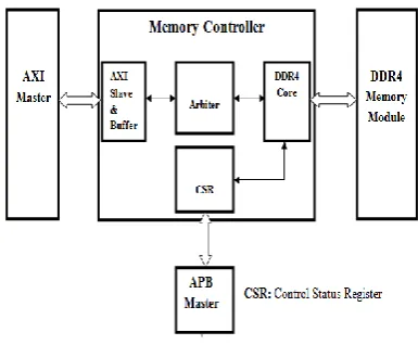
DDR4 memory controller accepts write/read requests from multiple masters and generates memory related commands for DDR4 memory to access memory. DDR4 memory controller acts as interface logic between processors and the DDR4 SDRAM memory and controls the flow of data going to and from the DDR4 memory. Its efficient design and implementation plays an important role in memory performance [3]. Figure 2 shows the proposed architecture for memory controller for DDR4 memory.
Copyright © 2015 IJECCE, All right reserved for DDR4 memory. DDR4 Core part of memory controller
has two units; time generation unit and command generation unit. Command generation unit reads the request from buffer and generates the commands for memory where as the timing generation unit generates time for the command generator for the proper operation. CSR stores the timing parameter for the DDR4 core in respective registers that is written by the APB Bridge.
Fig.2. Memory Controller Architecture
DDR4 is being used in real time applications where high speed processors and memories are required. DDR4 being the latest one, there is a need to design optimal number operational registers in the CSR within the memory controller to increase the speed of operation and to reduce the area requirement.
This paper mainly deals with the detailed design and description of an optimized CSR for the DDR4 memory controller. Also design of APB slave interface and the interface logic between the CSR and DDR4 core have been implemented in this work.
This paper is divided into the following sections. Section I is introduction and Section II contains the functional description of CSR. The design and implementation of CSR is described in section III, section VI is presents the simulation results and finally the conclusion is given in section V.
II.
D
ESIGN OFCSR
CSR is responsible for storing the timing parameter for the DDR4 core to generate the commands for the DDR4 memory and stores the status information about the read or write success/failure. Totally 21 control registers were designed as per the JEDEC specification and 7 mode registers by JEDEC spec are used to store the timing parameters and different mode operation for the DDR4 memory, each register is of 32bit wide and stores the timing information for the DDR4 core.
DDR4 specification gives the specific timing requirements [1]. Consider the 1600MT/s (MT/s Mega Transaction per second) speed memory as an example. The parameter settings as per the JEDEC specifications are: tCK=8ns, tCCD=5nCK, AL=0, BL=8, CL=10,
WL=CWL=9, tWTR= max (4nCK, 6ns) =5,
tRTP=35ns=28.
Control registers are arrived based on the different timing parameter requirements for the command generation as per the JEDEC DDR4 SDRAM specification [1]. Calculate the number of bits required to store timing value for both 1600MT/s and 3200MT/s speed memory, and group this value into register of 32bit wide and give the proper address. The example given below shows how to calculate the number of bits required for storing the timing parameter for memory controller by considering both minimum and maximum speed memory. Let us first consider for 1600MT/s (Min) speed memory and calculate number of bits required to store the timing parameter tRRD_L (1K) (Activate to Activate command delay to same bank group for 1KB page size) as per the JEDEC specification.
tRRD_L (1K) = Max (4nCK, 6ns) = Max (4nCK, (6ns/1.25*10-09)) = Max (4nCK, (6ns *800 * 1006)) =Max (4nCK, 4.8) (requires 3 bits to store the decimal value 5) Similarly consider 2400MT/s (Max) speed memory and calculate number of bits required to store the timing parameter tWTR_S as per the JEDEC specification.
tRRD_L (1K) = Max (4nCK, 4.9ns) = Max (4nCK, (4.9ns/8.33*10-10)) = Max (4nCK, (4.9ns *1200 * 1006)) =Max (4nCK, 5.88) (requires 3 bits to store the decimal value 6)
Table I: Timing parameters and bit calculation for Command_And_Address Register
Description Symbol
Min. Speed 1600MT/s Max. Speed 1600MT/s No. of bits CAS_n to CAS_ n command delay for same bank group
tRRD_L (2K)
5nCK 6nCK 3
CAS_n to CAS_n command delay for different bank group tRRD_L (1K)
4nCK 4CK 3
Activate to activate command delay to different bank group for 2KB page size
tRRD_L (1/2K) Max(4nCK, 6ns) =(4nCK, 4.8) Max(4nCK,5 .3ns) =max(4nCK, 6.36) 3 Activate to activate command delay to different bank group for 2KB page size
tFAW_2 K Max(4nCK, 5ns) =(4nCK,4) Max(4nCK, 3.3ns =max(4nCK, 3.96) 3 Activate to activate command delay to different bank group for 1/2 KB page size
tFAW_1 K Max(4nCK, 5ns) =(4nCK,4) Max(4nCK, 3.3ns) =max(4nCK, 3.96) 3 Activate to activate command delay to same bank group for 2KB page size
Copyright © 2015 IJECCE, All right reserved Activate to
activate command delay to same bank group for 1KB page size
tWTR_S Max(4nCK,
6ns) =Max(4nC K,4.8) Max(4nCK, 4.9ns) =Max(4nCK , 5.88) 3 Activate to activate command delay to same bank group for 1/2KB page size
tWTR_L Max(4nCK,
6ns) =Max(4nC K,4.8) Max(4nCK, 4.9ns) =Max(4nCK, 5.88) 3 Four activate window for 2KB page size
tRTP 35ns =28 30ns =36 6
Similarly calculate number of bits for other timing parameters, considering both minimum and maximum speed memory as per JEDEC spec. Table I shows the example for calculating the number of bits required for the Command_And_Address register as per the JEDEC DDR4 SDRAM specification.
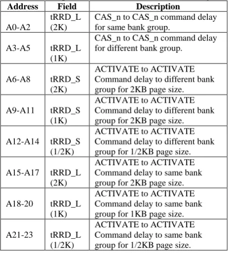
For register design consider number of bits for maximum speed (2400MT/s) so that it can store the value of lower speed memory.Based on the timing requirements for DDR4 memory registers arrived are Command_ And_Address register, CS_n_to_CAL register, DRAM_ Data_Timing register, Data_Strobe_Timing register, MPSM_ Timing register, Calibration_Timing register, Reset/Self_Refresh register, Power_down_ timing register, PDA_Timing register, ODT register, Write_Leveling register, CA_Parity_Timing register, CRC_Error_ Reporting register, Geardow_timing register, tREFI register, different mode registers includes MR0, MR1, MR2, MR3, MR4, MR5 and MR6 registers. Table II shows an example for Command_ And_ Address register with their field and description.
Table III and IV show the field and description of DRAM_Data_Timing and Power_Down_Timing registers. Table II: Description of Command_And_Address register
Address Field Description
A0-A2
tRRD_L (2K)
CAS_n to CAS_n command delay for same bank group.
A3-A5 tRRD_L (1K)
CAS_n to CAS_n command delay for different bank group.
A6-A8 tRRD_S (2K)
ACTIVATE to ACTIVATE Command delay to different bank group for 2KB page size.
A9-A11 tRRD_S (1K)
ACTIVATE to ACTIVATE Command delay to different bank group for 2KB page size.
A12-A14 tRRD_S (1/2K)
ACTIVATE to ACTIVATE Command delay to different bank group for 1/2KB page size.
A15-A17 tRRD_L (2K)
ACTIVATE to ACTIVATE Command delay to same bank group for 2KB page size.
A18-20 tRRD_L (1K)
ACTIVATE to ACTIVATE Command delay to same bank group for 1KB page size.
A21-23 tRRD_L (1/2K)
ACTIVATE to ACTIVATE Command delay to same bank group for 1/2KB page size.
A24-29 tFAW
Four activate window for 2KB page size.
A30-31 RFU Reserved for future use (RFU)
Table III: Description of DRAM_Data_Timing register
Address Field Description
A0-A3 tDQSQ DQS_t, DQS_c to DQ skew, per group, per access tDQSQ. A4-A7 tDQSQ DQS_t, DQS_c to DQ Skew
deterministic, per group, per access –tDQSQ.
A8-A11 tQH DQ output hold time from DQS_t, DQS_c tQH.
A12-A15 tQH DQ output hold time deterministic from DQS_t, DQS_c –tQH A16-A19 tDQSQ DQS_t,DQS_c to DQ Skew total,
per group, per access; DBI enabled-tDQSQ
A20-A23 tQH DQ output hold time total from DQS_t, DQS_c; DBI enabled –tQH A24-A27 tDQSQ DQ to DQ offset , per group, per
access referenced to DQS_t, DQS_c –tDQSQ
A28-A31 RFU Reserved for future use (RFU)
Table IV. Description of Power_Down_Timing Register
Address Field Description
A0-A2 tXP Exit Power Down with DLL on to any valid command.
A3-A5 tCKE CKE minimum pulse width A6-A7 tCPDED Command pass disable delay A8-A10 tPD Power Down Entry to Exit
Timing.
A11-A12 tACTPDEN Timing of ACT command to Power Down entry
A13-A14 tPRPDEN Timing of PRE or PREA command to Power Down entry. A15-A20 tRDPDEN Timing of RD/RDA command to
Power Down entry. A21-A27 tWRPDEN Timing of WR command to
Power Down entry (BL8OTF, BL8MRS, BC4OTF). A28-A31 tMRSPDEN Timing of MRS command to
Power Down Entry.
III.
D
ESIGN ANDI
MPLEMENTATIONThis work was carried out at Graphene Semiconductor Services Pvt. Ltd. It has been successfully designed, implemented and verified.
Control registers are designed to store the timing parameter required to generate commands for DDR4 memory. Status register stores the information regarding memory read or writes success/failure.
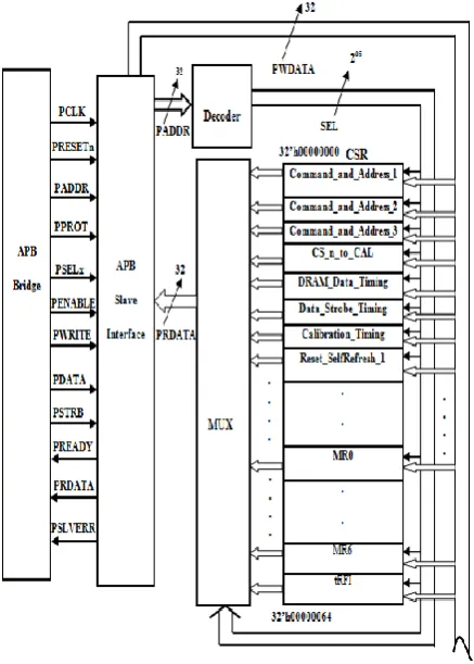
Copyright © 2015 IJECCE, All right reserved APB Bridge writes data into the control register when
the PSEL and PENABLE signals are set to logic high. Address and data are available on PADDR and PWDATA bus respectively. In response to this, slave generates PREADY signal indicating the start of transaction. Then the data on PWDATA bus is captured on positive edge of PCLK as shown in figure 4 and is stored into the respective control register.
Fig. 3 CSR update through APB slave interface
All the control and mode registers are provided with status register. When the control and/or mode register is updated with the new value the corresponding status bit in the status register is set to logic one, which indicates that the DDR4 core that registers are updated with the new value; otherwise status bit will reset to zero. Figure 6 shows the state diagram for operational activity of APB protocol.
Fig.4. Read Transfer Operation
Fig.5. Write Transfer Operation
Fig. 6 State diagram showing operational activity of APB protocol
DDR4 core of memory controller has command and time generation unit. Time delay between one command to next active command is stored in the control registers. During command generation, timing unit reads this value from the respective control register and loads it into the counters for the proper operation. After the read or write operation on DDR4 memory, the status register is updated with read/write success/ failure information.
IV.
S
IMULATIONR
ESULTSThis section presents the results of proposed work for different test cases. The entire design has been coded in SystemVerilog HDL language and simulated using ModelSim 10.1c version.
Copyright © 2015 IJECCE, All right reserved
Fig.7. Simulation result of APB slave interface
Fig.8. Writing into Control Register through APB
slave interface
Fig.9. Control Register updates through APB slave
interface
The figures 8 to 10 show the CSR read and write operation through APB slave interface in various modes, and also shows control registers updated with the data from PWDATA bus.
DDR4 core reading the data from the control and mode registers for the WRITE command generation and updating the values into the respective counters of the timing unit, this operation is as shown in figure 11. Figure 12 shows the status bit is set to logic one when registers is updated with the new data which indicates the DDR4 core, so that DDR4 core can read the new updated value.
Fig.10. Snapshot showing the write and read with
CSR and status bit updates
Fig.11. DDR4 core read timing values from control
and mode registers for WRITE command generation
PREADY
PWDATA
Copyright © 2015 IJECCE, All right reserved
Fig.12. Status bit Update when registers are updated
with new data
V.
C
ONCLUSIONIn the proposed work, Control Registers are designed according to JEDEC DDR4 SDRAM specification. From the results obtained, it is concluded that APB master successfully writes the timing parameter data into the control registers and also successfully reads the response from the CSR. When CSR register is updated with new value corresponding status register bit is successfully set to logic one indicating the DDR core that CSR register is updated with the new value or else reset to zero. Status register is successfully updated with the status on each read/write success/failure.The results also show that the DDR4 core is successfully reading the timing parameter from CSR for the command generation and loading this value into the counter logic.
The improvement that can be incorporated in this work is error detection and correction of message using CRC (Cyclic Redundancy code) and status register.
R
EFERENCES[1] JEDEC solid state technology association, “DDR4 SDRAM
Specification (JESD79-4)”, JEDEC Standard, pp.1-203,
September 2012.
[2] Md. Ashraful Islam, Md. Yeasin Arafath, and Md. Jahid Hasan,
“Design of DDR4 SDRAM Controller”, 8th International Conference on Electrical and Computer Engineering (ICECE), pp.148-161, 20-22 December 2014.
[3] Pan Guoteng, Luo Li, Ou Guodong, Dou Qiang, Xie Lunguo,
“Design and Implementation of a DDR3-based Memory Controller”, PP: 540-543, Third International Conference on Intelligent System Design and Engineering Applications (ISDEA), IEEE, pp.540-543, Hong Kong, 16-18 Jan2013.
[4] Khaled Khalifa, Haytham Fawzy, Sameh El-Ashry, Khaled
Salah, “A Novel Memory Controller Architecture”,
Electrical/Electronic Computer Telecommunications and
Information technology (ICTI-CON), pp.1-4, 14-17 May 2014.
[5] Pooran Singh, Bhupendra Reniwal, Vikas Vijayvargiya and
Santosh Kumar Vishvakarma, “Design of high speed DDR SDRAM controller with less logic utilization”, 2nd International
Conference on Devices, Circuits and Systems (ICDCS), pp.1-6, Combiatore, 6-8 March 2014.
[6] Vikky Lakhmani, Nusrat Ali, Dr. Vijay Shankar Tripathi, “AXI
Compliant DDR3 Controller”, Second International Conference on Computer Modeling and Simulation (IEEE), China, vol.4, pp.391-395, 22-24 January, 2010.
[7] ARM Limited, “AMBA APB protocol specification (Version:
2.0)”, A manual, 13 April 2010.
[8] Chris Spear, “SystemVerilog for verification”, 2nd edition,
Spinger publications, 2012.
[9] Design Automation Standards Committee of the IEEE Computer
Society and IEEE Standards Association Corporate Advisory Group, “IEEE Standard for SystemVerilog, Unified Hardware Design, Specification, and Verification Language”, IEEE, pp.1-453, 21 February 2013.
[10] http: www.google.com
A
UTHOR’
SP
ROFILEMr. Sathish D.
Did his B.E from EWIT, Bengaluru, Karnataka, India and M.Tech in VLSI Design and Embedded Systems from the Dept. of ECE Engg. BNMIT Bengaluru, Karnataka, India. This paper is based on the project work carried out at Graphene Semiconductor Pvt. Ltd. under the guidance of Dr. P.A. Vijaya and Mr. Ramudu B.
Dr. P. A. Vijaya
Did her B.E. from MCE, Hassan and M.E. and Ph.D. from IISc, Bengaluru. She worked in MCE, Hassan, Karnataka, for about 27 years. Presently, she is a Professor in the Dept. of E&C Engg, BNMIT, Bengaluru, Karnataka, India, from 2013. Three students have obtained Ph.D degree under her guidance and four more are doing Ph.D. Her research interests are in the areas of Pattern Recognition, Image Processing, VLSI Design, Embedded Systems and RTOS.