37Pb AND 58Sn-42In SOLDERS
BY
Omah A.D, Obikwelu D.O.N, Ezema I.C
[email protected] [email protected] [email protected]
Department of Metallurgical and Materials Engineering, University of Nigeria Nsukka. (UNN)
ABSTRACT
The toxicity of lead during industrial production of components and the ecological damage caused by lead containing compounds has made the use of lead in solders undesirable. Hence, the emphasis of this research is to develop a solder that has unique material properties (like the conventional lead solder) using indium as a sub stitute to lead. Lead-bearing solder (63Sn-37Pb) and lead-free solder (58Sn-42In) alloys were developed and subjected to the same test analysis under the same test conditions so as to analyze and compare results. Both solders are low temperature alloys. The choice of any solder by industries depends on the ability of the solder to wet the materials it joins. Consequent upon this, a copper grid plate was used to conduct different wettability tests. The wetting time for lead bearing solder and lead -free solder are 4.7 and 5.9 seconds respectively while their corresponding contact angles in degrees are570 and 610. The final wettability test conducted was on the wetting area. The respective wettability values (in percentage) of the total area of the copper grid covered by the molten solder are: 8.3%, and 8.6% The alloy also have the following Vicker’s Hardness Values of 18.58VHN and 16.32VHN. The microstructures of the developed alloys were studied and analyzed. The alloy’s microstructures show that they are all eutectic compositions.
Key words: Lead-free, wettability, solder, microstructure
1.0 INTRODUCTION
Most metals are not used in their pure form; they are combined with other metallic or non -metallic elements to form an alloy. By combining the elements in various proportions, it is possible to obtain a material with specific properties. Tin forms binary system with many other metals and non -metals, the most well known are soft solders. [1]
Tin with lead and tin with indium are all eutectic alloys. Tin is the active element in most solders. Other alloying elements have the primary function of lowering the liquidus temperature and also serve as mere filler. The introduction of some alloying elements also improves the mechanical properties of the solders. [1]
The metals that are candidates as substitute constituents in lead -free alternative
solder alloys must be judged not only on compatibility with performance requirements, but also on the basis of availability and subsequent cost. Substitute metals such as copper, silver, bismuth and indium have anticipated source availability on the order 20-40 years, given present rates of mining of known sources and use. [2] The as -solidified microstructure of a typical eutectic depends on the rate of cooling. Relatively slo w cooling produces the classic eutectic microstructure in which the two constituent phases alternate within reasonably well -defined colonies or cells. Rapid solidification may inhibit the form of the eutectic structure, producing a fine-grained mixture of the two phases. Both conditions occur in the manufacture of solder joints. [3]
NIGERIAN JOURNAL OF TECHNOLOGY, VOL. 29 NO 2, JUNE 2010 shape taken up by the droplet depends on the
relative magnitude of the molecular forc es that exists within the liquid (cohesive forces) and between the liquid and solid (adhesive forces). The index of this interaction is the wetting (contact) angle, “θ”, defined as the angle between a tangential line at which a liquid meets another surface. [1]
The wetting property of a material (solder) on a base metal (substrate) is categorized by two aspects; namely: the degree of wetting and the speed of wetting. The degree of wetting refers to how far the alloy spreads and is an equilibrium situation controlled by the laws of thermodynamics of surfaces where the surface and interfacial tensions of the liquid and solid are involved. The speed of wetting refers to the rate (i.e. how fast) the solder wets and spreads. However, this is controlled by a combination of several factors; namely the thermal demand of the system, the use of flux and the chemical reactions at the interfaces. [1]
Greater percentage of the work done by other researchers lies on the study of the mechanical behavior of the solder joi nt. The wettability test conducted lies more on the contact angle of the lead bearing solder and lead free solder. Much has not been done on the wetting time and the spreading power of these solders alloys. A simple wettability test using copper grids to d etermine the wetting time and spreading (bonding) power of these alloys is therefore part of the emphasis of this research work. The microstructure of these solders and not those of the sol der joints were also studied.
2.0 MATERIALS AND METHODS
2.1 Materials
The metals used for the production of the above alloys are granulated Tin, Indium and Lead. They all have purity of 99% with traces of impurities like: Arsenic (As) = 0.0001%; Bismuth (Bi) = 0.002%; Copper (Cu) =
0.02%; Antimony (Sb) = 0.02%; Iron ( Fe) = 0.01%; Acid insoluble matter = 0.05%; Calcium (Ca) = 0.002%; Lead (Pb) = 0.02%; Magnesium (Mg) = 0.002%; Potassium (K) = 0.002%; Sodium (Na) = 0.002%. Some of the materials used for this research work include the following: electric furnace for melti ng the metals for alloy formation; moulding boxes; Cope, drag, sand, risers, sieve, shovel, ram, e.t.c.; Weighing Balances, digital camera, 50X45X6mm copper plate, stop watch, tape rule, pencil, Hardness Tester, File, handsaw, silica carbide paper of diffe rent grids, Grinding/Polishing machine, Metallurgical Microscope, and etching reagents.
2.2 Methods
2.2.1 Alloying and Casting
Moulds for the alloys to be produced were made and allowed to dry properly before casting. Different quantities of the metals as determined by the charge calculation were measured out and charged into the crucible pot starting with the metal of higher melting temperature. When this has melted, the metal with the lower melting point was then charged into the crucible. The charges were continuously stirred to ensure homogeneity of the molten alloy. After this the molten alloy was poured into the mould. After solidification and cooling, the alloys were removed and cut into different sizes for different tests to be carried out.
2.2.2 Sample Preparation
Generally sample preparation involves the following: cutting, grinding, polishing, and etching with a suitable reagent. [4, 5]
NIGERIAN JOURNAL OF TECHNOLOGY, VOL. 29 NO 2, JUNE 2010 operation on the flat file was continued until
the surfaces became flat and free from all scratches due to the hack saw.
Intermediate and fine polishing operations were then carried out on silicon -carbide papers of progressively finer grade. The first grid used was 60 followed by 120, 220, 320, 400, 500, 600, 1200, 2200, and 4000 silicon carbide papers. The final polishing operation was carried out using a rotating cloth pad impregnated with a conductive paste mixed with DP suspension. This final polishing operation was to bring out the mirror-like surface.
The specimens were washed free of any adhering polishing compound using distil water; after which they were etched by smearing (rubbing) the surface of the specimen with a piece of cotton wool soaked with the etchant. After the etching operation, the specimens were quickly plunge d into distil water to wash away the etchant, and then examined to see the extent of etching. The time used for etching varied with different alloys and etching reagents.
2.2.3 Micrograph
Examination of the etched alloys under the metallurgical microscope revealed the microstructure of the alloys at different magnifications. The photomicrographs of the structures observed were shown in the results.
2.2.4 Mechanical Testing
2.2.4.1 Hardness Testing
The hardness test specimens were prepared using the same techniques used for specimens prepared for microstructure except that the etching operation was not carried out. ESEWAY Hardness Tester was used to determine the Vickers Hardness Number (VHN) of the alloy samples. The specimen was placed on the anvil and the spindle was rotated until the specimen came in contact with the indenter. The variable slits were adjusted to be at the edges of the pyramid – shaped impression after which the ocular readings obtained were converted to Vickers‟ Hardness Number using the Vickers‟ Chart.
2.2.5 Measurement of Contact Angle
The contact angle was determined by drawing tangent to the drop profile at the point of three – phase contact on the drop profile photograph [6, 7]
Ten grams of each alloy was melted and poured on the copper grids. It was allowed to spread and solidify. The total number of squares covered by the alloy and the percentage of the number of squares covered were calculated from the expression: [8 ]
1 100 squares of number total
covered squares of number covered
squares of
percentage
2.2.6 Wetting Time
NIGERIAN JOURNAL OF TECHNOLOGY, VOL. 29 NO 2, JUNE 2010
3.0 RESULTS AND DISCUSSION
3.1 Results 3.2
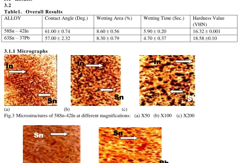
Table1. Overall Results
ALLOY Contact Angle (Deg.) Wetting Area (%) Wetting Time (Sec.) Hardness Value (VHN)
58Sn – 42In 61.00 0.74 8.60 0.56 5.90 0.20 16.32 0.001 63Sn – 37Pb 57.00 2.32 8.30 0.79 4.70 0.37 18.58 0.10
3.1.1 Micrographs
(a) (b) (c)
Fig.3 Microstructures of 58Sn-42In at different magnifications: (a) X50 (b) X100 (c) X200
(a) (b)
Fig. 4 Microstructures of 63Sn- 37Pb at different magnifications: (a) X100 (b) X200
3.2 DISCUSSION
The wetting rate of Tin-Lead (63Sn-37Pb) is = 8.3% The alloy of tin and indium (58Sn – 42In) depicts a better wetting rate of 8.6% , Hence it can be concluded from this result that lead–free solder alloy (58Sn-42In) investigated can satisfactorily replace the lead bearing solder as far as their wetting power is concerned thereby helping to eliminate the poison‟s effect of lead.
It has been proved experimentally by researchers that small contact angle indic ates strong wetting power. The contact angle of the lead solder (63Sn – 37Pb) is 570, while
that of the 58Sn – 42In solder is 610which is very close to that of lead solder. The wetting time of tin–lead solder is 4.7s and 58Sn – 42In took a little longer to wet the copper substrate at 5.9s
The hardness results show that the Sn -In alloy is ductile in nature and will be able to withstand mechanical shocks like the tin – lead solder in different applications. Hence, it can be concluded that they can satisfa ctorily replace the lead bearing solder.
3.2.1 Microstructure
Sn
Pb
Sn
Pb
In
Sn
In
Sn
In
NIGERIAN JOURNAL OF TECHNOLOGY, VOL. 29 NO 2, JUNE 2010 The 58Sn-42In microstructure is also a
mixture of two phases: The darker areas are the Indium phase while the lighter areas are the Tin phase. There is also a homogenous distribution of indium partic les in the tin matrix. It is a eutectic composition. The dark and light areas of the 63Sn – 37Pb micrograph are the tin rich and lead rich phases. The microstructure is a fine uniform two phased structure. Its fineness gives the alloy the characteristics of a ductile system and additional strength. It is a eutectic composition.
Comparing the microstructure of the eutectic Tin–Lead solder and that of Sn-In solder developed; it can be seen that the microstructure of each alloy reveals uniformity in the grain distribution. They are eutectic compositions.
4.0 CONCLUSION
The results of this research reveal that the Tin-Indium solder has similar properties to that of the Tin-Lead solder and it depicted a better property as in the case of their wetting rate. Since the toxicity of lead is now a primary concern in different nations and industries the Tin-Indium solders developed can be used as a substitute for the tin –lead solder.
REFERENCES
1. Tan, A.C. “Tin and Solder Plating in the Semiconductor Industry” World Scientific Publications, Singapore, 1993. pp. 204, 210-213
2. Cindy Meton, “The Effect of Reflow Process Variables on the Wettability of Lead-Free Solders.” Journal of the Minerals, Metals and Materials Society (JOM), Vol. 45, Number 7. 1993 p p. 33 3. MORRIS, J.W. Jr., et-al “Microstructure
and Mechanical Properties of Sn -In and Sn-Bi Solders” Journal of the Minerals, Metals and Materials Society (JOM), Vol. 45, Number 7. 1993 pp. 25
4. Higgins, R.A. „‟Engineering Metallurgy 1‟‟ (Applied Physical Metallurgy). The Chaucer Press Ltd. Bungay Suffolk 1980 pp.147 – 175, 400 – 403.
5. Nwajagu, C.O., Ugwu, F.O.H. „‟Principles of Materials Science,‟‟ Computer Edge Publishers, Enugu, Nig. 1997 pp127-133
6. Kinloch, A.J. „‟Adhesion and Adhesive Science and Technology,‟‟ London: Chapman and Hall. 1987 pp. 1, 18 – 23 7. Bikerman, J.J. „‟The Science of Adhesive
Joints,‟‟ New York, Academy Press, 1961. pp. 33 – 41.