Chemistry Publications Chemistry
2014
Transition metals on the (0001) surface of
graphite: Fundamental aspects of adsorption,
diffusion, and morphology
David Victor Appy
Iowa State University, [email protected]
Huaping Lei
Iowa State University
Cai-Zhuang Wang
Ames Laboratory, [email protected]
Michael C. Tringides
Iowa State University, [email protected]
Da-Jiang Liu
Ames Laboratory, [email protected]
See next page for additional authors
Follow this and additional works at:http://lib.dr.iastate.edu/chem_pubs
Part of theChemistry Commons,Materials Science and Engineering Commons, and thePhysics Commons
The complete bibliographic information for this item can be found athttp://lib.dr.iastate.edu/ chem_pubs/99. For information on how to cite this item, please visithttp://lib.dr.iastate.edu/ howtocite.html.
Transition metals on the (0001) surface of graphite: Fundamental aspects
of adsorption, diffusion, and morphology
Abstract
In this article, we review basic information about the interaction of transition metal atoms with the (0001) surface of graphite, especially fundamental phenomena related to growth. Those phenomena involve adatom-surface bonding, diffusion, morphology of metal clusters, interactions with steps and sputter-induced defects, condensation, and desorption. General traits emerge which have not been summarized previously. Some of these features are rather surprising when compared with metal-on-metal adsorption and growth.
Opportunities for future work are pointed out.
Keywords
adsorption, diffusion, graphene, graphite, nucleation, transition metal, Ames Laboratory, Physics & Astronomy, Materials Science & Engineering, Chinese Academy of Sciences
Disciplines
Chemistry | Materials Science and Engineering | Physics
Comments
NOTICE: This is the author’s version of a work that was accepted for publication inProgress in Surface Science. Changes resulting from the publishing process, such as peer review, editing, corrections, structural formatting, and other quality control mechanisms may not be reflected in this document. Changes may have been made to this work since it was submitted for publications. A definitive version was subsequently published inProgress in Surface Science, 89 (2014), doi:10.1016/j.progsurf.2014.08.001.
Authors
David Victor Appy, Huaping Lei, Cai-Zhuang Wang, Michael C. Tringides, Da-Jiang Liu, James W. Evans, and Patricia A. Thiel
1
NOTICE: This is the author’s version of a work that was accepted for publication in Progress in Surface Science. Changes resulting from the publishing process, such as peer review, editing, corrections, structural formatting, and other quality control mechanisms may not be reflected in this document. Changes may have been made to this work since it was submitted for publications. A definitive version was subsequently published in Progress in Surface Science, 89 (2014), doi: 10.1016/j.progsurf.2014.08.001.
Transition Metals on the (0001) Surface of Graphite: Fundamental Aspects of Adsorption, Diffusion, and Morphology
by
David Appy,a,b Huaping Lei,a,c,e Cai-Zhuang Wang,a
Michael C. Tringides,a,c Da-Jiang Liu,a James W. Evans,a,c and Patricia A. Thiela,b,d
a
The Ames Laboratory, Ames, Iowa 50011 USA
b
Department of Chemistry, Iowa State University, Ames, Iowa 50011 USA
c
Department of Physics & Astronomy, Iowa State University, Ames, Iowa 50011 USA
d
Department of Materials Science & Engineering, Iowa State University, Ames, Iowa 50011 USA
e
Key Laboratory of Materials Physics, Institute of Solid State Physics, Chinese Academy of Sciences, Hefei 230031, China
Abstract.
In this article, we review basic information about the interaction of transition metal atoms with the (0001) surface of graphite, especially fundamental phenomena related to growth. Those phenomena involve adatom-surface bonding, diffusion, morphology of metal clusters, interactions with steps and sputter-induced defects, condensation, and desorption. General traits emerge which have not been summarized previously. Some of these features are rather surprising when compared with metal-on- metal adsorption and growth. Opportunities for future work are pointed out.
1.Introduction.
Graphite is an intriguing support for metals because of its inertness in
aggressive environments, as well as its low cost and high abundance. A major application for graphite-supported metals is lithium ion batteries [1, 2]. In fact, the demand for these batteries is expanding so quickly that it currently drives the international market in graphite [1]. An important application on the horizon is biofuel conversion, where graphite (or other carbon-based materials) may provide robust supports for catalysts in aqueous media [3].
Adsorption of transition metals and noble metals on graphite has been studied for many years—starting well before the discovery of graphene, carbon nanotubes, or even C60. Actually, adsorption of metals on graphite provides a benchmark and point of entry
for understanding metal interaction with these more-recently discovered forms of carbon. Even more broadly, graphite has been regarded as a good substrate for model investigations of surface phenomena, e.g. catalysis by supported metal particles [4].
2
NOTICE: This is the author’s version of a work that was accepted for publication in Progress in Surface Science. Changes resulting from the publishing process, such as peer review, editing, corrections, structural formatting, and other quality control mechanisms may not be reflected in this document. Changes may have been made to this work since it was submitted for publications. A definitive version was subsequently published in Progress in Surface Science, 89 (2014), doi: 10.1016/j.progsurf.2014.08.001.
3
NOTICE: This is the author’s version of a work that was accepted for publication in Progress in Surface Science. Changes resulting from the publishing process, such as peer review, editing, corrections, structural formatting, and other quality control mechanisms may not be reflected in this document. Changes may have been made to this work since it was submitted for publications. A definitive version was subsequently published in Progress in Surface Science, 89 (2014), doi: 10.1016/j.progsurf.2014.08.001.
phenomenological), but rather we focus on the fundamental aspects of the interaction of metal atoms with a graphite surface. These fundamental aspects include: (1) strength of the metal-carbon adsorption bond; (2) diffusion coefficient; (3) adsorption and desorption kinetics; (4) long-range electronic response of the substrate; (5) shapes of atomic
aggregates; and (6) the influence of defects.
It will also be informative to compare some of these aspects of metals on
graphite with those of metals on metals. For the latter, a broad understanding of mechanisms, kinetics, and thermodynamics of deposition, nucleation, and growth has been established [6-9]. To some extent, this conceptual framework is very useful and it can be applied to metals on graphite, but we will show that there are also significant differences. One example is the condensation coefficient as defined in Section 9. For a metal atom on a metal surface, at room temperature (nominally 300 K), this quantity can be safely assumed to be unity. For a metal atom on a graphite surface, there is
considerable evidence that this quantity is less than unity. Another example is the
diffusion barrier of a single atom. For metals on metals, diffusion barriers are typically a few tenths of eV, whereas for the same metals on graphite, diffusion barriers can be lower by an order of magnitude. Differences, such as these in condensation coefficient and diffusion barrier, can require widely different interpretive frameworks for
experimental data in the two types of systems.
In this article, we focus on metals deposited via physical vapor deposition, because this technique is most favorable for understanding metal deposition in terms of a sequence of simple atomic processes, beginning with impingement of single atoms at the surface. The subsequent sequence can then include diffusion of atoms, nucleation and growth of clusters, desorption, and/or interaction with step edges. There exists a considerable body of complementary work in which pre-formed metal clusters are deposited onto the graphite surface. Because that approach can provide a high level of control and surface homogeneity, it holds considerable promise for nanotechnology, but it is not emphasized here. Aspects of that body of work have been summarized elsewhere [10-12].
2.Overview of the experimental context.
Metals can be deposited on graphite using a wide variety of techniques, ranging from wet (chemical) methods to gas-phase methods [11, 13-16]. As mentioned in the Introduction, this article focuses on the method of physical vapor deposition, because in that process, single atoms impinge on the graphite surface, leading most directly to atomic-scale insights.
4
NOTICE: This is the author’s version of a work that was accepted for publication in Progress in Surface Science. Changes resulting from the publishing process, such as peer review, editing, corrections, structural formatting, and other quality control mechanisms may not be reflected in this document. Changes may have been made to this work since it was submitted for publications. A definitive version was subsequently published in Progress in Surface Science, 89 (2014), doi: 10.1016/j.progsurf.2014.08.001.
5
NOTICE: This is the author’s version of a work that was accepted for publication in Progress in Surface Science. Changes resulting from the publishing process, such as peer review, editing, corrections, structural formatting, and other quality control mechanisms may not be reflected in this document. Changes may have been made to this work since it was submitted for publications. A definitive version was subsequently published in Progress in Surface Science, 89 (2014), doi: 10.1016/j.progsurf.2014.08.001.
(shown in Fig. 1) are commonly reported, especially using STM [17-21]. Examples of micron-wide terraces, and atomic-scale resolution are shown in Fig. 2(a-b). In fact, because of HOPG's atomic-scale perfection in air, undergraduate laboratory experiments have been designed to image graphite or modified graphite surfaces with scanning probe microscopies, e.g. [22-24].
However, graphite is not completely inert. In a study of Au deposition in the 1960s, it was already reported that exposure to water or cleaning solvents had a strong effect on the density of Au clusters on graphite, based on electron microscopy [25]. In the 1970s, it was found that Au nucleation and growth is significantly different on graphite that has been cleaved in UHV, than on graphite cleaved and allowed to rest in air for several hours [26]. In fact, the density of Au nuclei depends systematically upon the time that a cleaved graphite surface spends in air before Au is deposted upon it [27]. These observations are probably explained by the adsorption of hydrocarbons, which causes the surface properties of graphene and graphite to change during exposure to air (over a few tens of minutes) [28]. Presumably, the hydrocarbons are too mobile to be imaged
effectively with scanning probe techniques, at least at the typical observation temperature of 300 K, so the surface may appear deceptively clean when analyzed with such
techniques.
Independent of the environment's effect on the graphite substrate, environment may affect the chemical state of the metal or the distribution of metal on the surface during or after deposition, especially via oxidation or via enhancement of restructuring rates [29]. Recently, for instance, it has been reported that exposure to CO(g) accelerates coarsening of Pd nanoclusters on a graphene surface [30]. In short, there are many reasons to be skeptical about the total inertness of metal-on-graphite systems, and to value UHV as a component of these experimental studies.
There are various grades and sources of graphite. Highly-oriented pyrolytic graphite (HOPG) is a synthetic form available in large samples with high purity and high structural perfection. (A synthetic form of graphite known as Kish graphite, with lower purity and smaller sample size, can be considered the historical precursor of HOPG [31].) The highest-quality material is employed in X-ray and neutron optics, where the
structural quality of HOPG is judged by its mosaic spread. Grades are usually designated ZYH, ZYB, and ZYA, with ZYA having the smallest mosaic spread (0.4o + 0.1o) and largest grain size (up to 3 mm) [31].
HOPG cleaves easily along the basal plane. A fresh surface is prepared by
6
NOTICE: This is the author’s version of a work that was accepted for publication in Progress in Surface Science. Changes resulting from the publishing process, such as peer review, editing, corrections, structural formatting, and other quality control mechanisms may not be reflected in this document. Changes may have been made to this work since it was submitted for publications. A definitive version was subsequently published in Progress in Surface Science, 89 (2014), doi: 10.1016/j.progsurf.2014.08.001.
correlation to HOPG grade. The latter values correspond to 5 x 10⁻¹⁰ to 5 x 10⁻⁶ defects per C atom in the surface plane.
Even in the most careful studies, graphite is usually cleaved in air and then transferred to UHV, rather than being cleaved in situ. Following transfer, the surface is often heated before metal is deposited. The highest reported cleaning temperature, in UHV, is 2500 K [49, 50]. Metois, Heyraud and Takeda [27] have reviewed studies of various procedures for cleaning HOPG by thermal annealing. In our own work, we have experimented with thermal treatments in the range 300 K to 1300 K, and have found that heating ZYA or ZYH to 800 K for several tens of minutes in UHV is effective.
Because fundamental energetic and mechanistic information is our objective, this review relies most heavily on experimental studies from the recent literature where deposition and analysis were conducted entirely and continuously in UHV, although some papers from other types of experiments are also noted.
As a final comment, in our experience, metals on graphite surfaces are
surprisingly difficult to work with, using scanning probe techniques. This is because the tip interacts strongly with the metal particles. The reason for this is discussed further in the following section. Consequently, tip stability and experimental reproducibility can be more challenging than in metal-on-metal experiments. Tip effects are illustrated in Fig. 3. 3.Bonding of a metal adatom to the basal plane.
Theory is the source of all information currently available about the adsorption energy (Ea) of metal atoms on graphite. However, two comments about the theoretical
landscape are relevant. First, a number of papers nominally model metal adsorption on graphite, but they use a single sheet of sp2-hybridized carbon to model the carbon surface. Hence, they are more appropriately regarded as models of free-standing graphene than
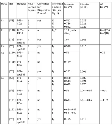
graphite. This is especially true of work that was conducted before the experimental characterization of graphene in 2004 [32, 33]. Table 1 summarizes values of adsorption energy for several metals. Only a small number of results are shown, because we apply a filter to the literature: models must incorporate two or more carbon sheets in order to be included in this Table.
Second, it is known that London dispersion forces are important in the bonding between graphite sheets. However, before the late 2000's, it was not common to include dispersion forces in DFT. Perhaps for this reason, some theoretical papers reported that a metal atom's adsorption energy was the same, regardless of whether one carbon sheet or multiple carbon sheets were used as the model of graphite [51, 52]. But the values for Cr and Au in Table 1, from the work of Hardcastle et al. [53], clearly show that the metal atom's adsorption energy increases significantly as the number of carbon sheets increases from 1 to 3 when dispersion forces are included. Hence, results for metals on (1-layer) graphene cannot be simply transposed to graphite. Instead, the adsorption energy for a metal on graphene sets the lower limit on the value for graphite.
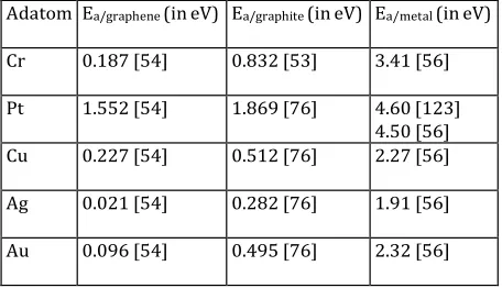
Table 2 compares good values (selected in accord with the discussion above) for adsorption energies of metal adatoms at optimal sites on three substrates: single-layer graphene (Ea/graphene), graphite (Ea/graphite), and the densest low-index surface of the
respective metal (Ea/metal). Note that, for the fcc or hcp metals, Ea/metal is the binding
7
NOTICE: This is the author’s version of a work that was accepted for publication in Progress in Surface Science. Changes resulting from the publishing process, such as peer review, editing, corrections, structural formatting, and other quality control mechanisms may not be reflected in this document. Changes may have been made to this work since it was submitted for publications. A definitive version was subsequently published in Progress in Surface Science, 89 (2014), doi: 10.1016/j.progsurf.2014.08.001.
natural three-fold hollow growth site. For the bcc metal Cr, Ea/metal is the binding energy
at the long-bridge site of the (110) surface, which is expected to be the preferred site. Table 2 shows that a simple qualitative relationship holds true for the 5 metals:
Ea/graphene < Ea/graphite < Ea/metal
(1)
This relationship can probably be applied as a check on the reasonableness of measured or calculated values of Ea/graphite for metals not included in the Table. To do this, of
course, one needs access to reliable values for Ea/graphene and Ea/metal. Values of Ea/graphene
are available elsewhere [54, 55]. With regard to Ea/metal, this is relatively simple to
calculate but it has not been tabulated elsewhere and values are in fact difficult to find in the literature. Therefore, we have calculated several values and collected them in Table 3, as a convenient reference [56].
Because Ea/graphene sets the lower limit in Eq. (1), we briefly review its trends
among 3d metals [54, 55]. First consider the variation along a single row. For the first- row 3d-transition metals V through Ni, Ea/graphene falls in the range 0.87-1.54 eV except for
Cr and Mn. The values for the latter two metals define a deep minimum (corresponding to weak binding) at only 0.18 and 0.16 eV, respectively. Next consider the metals in a single column, group 10: Ni, Pd, Pt. For these metals, Ea/graphene ranges from 1.08 to 1.55
eV, i.e. within the same range as most of the first-row transition metals. Finally, consider the coinage metals, group 11: Cu, Ag, and Au. Here, the interaction with graphene is very weak, only 0.02 to 0.23 eV. Based upon this information, the variation in absolute value across a row is greater than the variation within a column. Specifically, the variation across the first row is 1.38 eV, much greater than the variation in groups 10 and 11, which is only 0.47 and 0.21 eV respectively. Metals near half-filled d-shells (Cr, Mn) and formally filled d-shells (Cu, Ag, Au) have adsorption energies below 0.25 eV, and
interact more weakly with graphene than do other metals. In fact, the metals with
adsorption energies below about 0.5 eV can be described as physisorbed, while the others are chemisorbed [57]. Of course, calculations (and measurements!) for more transition metals on graphene will surely emerge to test and refine these generalizations.
For the chemisorbed metals, bonding with the graphene surface is covalent. The bonding-induced change in electron density is mainly localized on the carbon atoms closest to the metal adatom [54, 55]. Among the physisorbed metals, Au exhibits net electron transfer from the substrate to the metal adatom, in keeping with the fact that Au is a very electronegative metal [58, 59].
As stated in Eq. (1), bonding of metal adatoms with graphite is stronger than bonding with graphene, but to first order, one expects the trends in Ea noted above to be
similar for graphite. The reason for the higher adsorption energies on graphite is undoubtedly related to the dispersion forces which bind the carbon sheets, as noted by Hardcastle et al.[53]. However, no detailed analysis is available (to our knowledge) and this topic is ripe for detailed analysis.
8
NOTICE: This is the author’s version of a work that was accepted for publication in Progress in Surface Science. Changes resulting from the publishing process, such as peer review, editing, corrections, structural formatting, and other quality control mechanisms may not be reflected in this document. Changes may have been made to this work since it was submitted for publications. A definitive version was subsequently published in Progress in Surface Science, 89 (2014), doi: 10.1016/j.progsurf.2014.08.001.
9
NOTICE: This is the author’s version of a work that was accepted for publication in Progress in Surface Science. Changes resulting from the publishing process, such as peer review, editing, corrections, structural formatting, and other quality control mechanisms may not be reflected in this document. Changes may have been made to this work since it was submitted for publications. A definitive version was subsequently published in Progress in Surface Science, 89 (2014), doi: 10.1016/j.progsurf.2014.08.001.
the desorption barrier of Cu on graphite converged to the enthalpy of vaporization of bulk Cu at a Cu coverage of about 3 layer-equivalents. Deviation to smaller desorption
energies at lower Cu coverage was ascribed to the increasing deviation of smaller Cu clusters from bulk metal.
In another type of measurement, the contact angle between annealed, near- hemispherical Au clusters and the HOPG surface was measured using scanning electron microscopy [60, 61]. This yielded a value for the interaction energy of 0.26 eV per Au atom at the interface. However, one expects this value to be lower than the adsorption energy of a single Au adatom on HOPG. This expectation is consistent with the
calculated values for Ea/graphite of Au adatoms in Table 1, all of which are above 0.26 eV.
The basal plane of graphite is shown schematically in Fig. 1, with high-symmetry sites labeled. The possible high-symmetry adsorption sites on the basal plane of graphite are the same as on graphene—hollow (H), bridge (B), and top (T)—with one exception. On graphite there are two types of T sites, due to the ABAB stacking of the carbon sheets. In the Tα site, a carbon atom in the second layer sits directly beneath a carbon atom in the top layer, whereas in the Tβ site, the second layer is empty. The best
calculations available at present (Table 1) show that the favored site of a Cr adatom is H, of a Pt adatom is B (bridge, also called bond center), and the site of Ag, Au, and Cu adatoms is Tβ. The prediction of the Tβ site for Au is confirmed by experimental results [53, 62].
The relatively weak interaction between metals and graphite may be related to the common observation of time-dependent changes during STM imaging of these surfaces [62-67]. For example, Clark et al.[64] reported that a small 2D Pt cluster on graphite moved by tens of nm, relative to a defect site, from one image to the next. It is difficult to determine the extent to which such changes are tip-induced, or represent intrinsic
dynamic phenomena at the surface. In either case, however, one expects motion and instability to be facilitated by the relatively low value of Ea/graphite.
The issue of intercalation of metals in graphite also relates to surface adsorption. It is known that adsorbed metals—not only transition metals, but also other types of metals—can be buried beneath sheets of supported graphene, e.g. [68-73]. It is also known that some non-transition metals can intercalate in graphite surfaces, e.g. [74, 75]. However, we know of no evidence for intercalation of transition metal atoms in graphite
surfaces, at least under the conditions typical of surface science experiments. There is no obvious reason why intercalation of transition metals should not occur, at least at
sufficiently high temperature and high metal supersaturation. However, this possibility has rarely (if ever) been entertained when interpreting surface data for adsorption of transition metals on graphite.
4.Surface diffusion.
To a good approximation, the diffusion barrier on graphite (and graphene) can be equated to the minimum difference in adsorption energies between the favored sites, and high-symmetry locations between favored sites along physically-accessible pathways. This value, ⊗E, has been calculated for a few metals on graphite (Table 1).
1
NOTICE: This is the author’s version of a work that was accepted for publication in Progress in Surface Science. Changes resulting from the publishing process, such as peer review, editing, corrections, structural formatting, and other quality control mechanisms may not be reflected in this document. Changes may have been made to this work since it was submitted for publications. A definitive version was subsequently published in Progress in Surface Science, 89 (2014), doi: 10.1016/j.progsurf.2014.08.001.
those in Ea,graphite. For instance, ⊗Egraphite is highest for the strongly-bonded metal Pt,
and lowest for the weakly-bonded metal Ag.
Furthermore, the diffusion barrier for a metal on graphite consistently falls below the corresponding metal-on-metal diffusion barrier, but it can be either higher or lower than its diffusion barrier on graphene. For example, for the strongly-bound metal Pt,
⊗Egraphite = 0.16 eV (Table 1), which is lower than the value ⊗Egraphene = 0.19 eV
[54]. By contrast, for Cu, ⊗Egraphite = 0.02 eV (Table 1), which is much higher than
the value ⊗Egraphene = 0.004 eV [54]. These trends can be summarized as: ⊗Egraphene
⊗Egraphite < ⊗Emetal.
There are some experimentally-derived values for the diffusion barrier of metals on HOPG, but these are rather inconsistent. Ganz et al. reported ⊗E > 0.65 eV for isolated Ag adatoms and ⊗E > 0.8 eV for isolated Au on HOPG. This was derived from the lifetimes of a few species thought to be isolated metal atoms, using STM [62]. However, this is unreasonable, since then for these systems ⊗E >> Ea/graphite where
Ea/graphite = 0.28 eV for Ag and Ea/graphite = 0.50 eV for Au according to Table 1.
Furthermore, Anton et al. estimated the difference Ea/graphite-⊗E = 0.40 eV for Au on
HOPG [77-79]. To achieve this, they derived the mean diffusion length of an Au atom (before desorption), from densities of metal islands imaged with TEM. Invoking the data of Arthur and Cho [49] to estimate an upper limit of Ea/graphite, Anton et al. could then set a
limit of ⊗E < 0.24 eV for Au [77]. This limit is consistent with all of the calculated values shown in Table 1, but it is not consistent with the work of Ganz et al. [62]. Thus, it is doubtful that the rather high estimates of diffusion barrier for Ag adatoms (⊗E > 0.65 eV) and Au adatoms (⊗E > 0.8 eV) [62] are correct..
Diffusion of metal clusters, rather than single metal atoms, is also possible. On some metal surfaces, diffusion of small metal clusters containing several metal atoms is known [9, 80], and is sure to be facilitated even further by the relatively weak binding between metals and graphite. In two interesting studies, large, spherical, size-selected clusters of Au and Pt—containing hundreds or even thousands of atoms—were deposited on graphite. These large clusters were observed to diffuse and (at least for Au) coalesce at 300 K [81, 82]. Diffusion of smaller clusters that form by aggregation of individual atoms on the surface may be similarly feasible, provided that the cluster shape is reasonably compact.
5.Morphology of metal clusters on graphite.
Kern et al. have derived an approximate energetic criterion by which 2D vs. 3D growth can be predicted under conditions of thermodynamic equilibrium [8]. In terms of the variables we have defined, the condition for 3D growth is
Ea/graphite < Ea/metal (2)
1
NOTICE: This is the author’s version of a work that was accepted for publication in Progress in Surface Science. Changes resulting from the publishing process, such as peer review, editing, corrections, structural formatting, and other quality control mechanisms may not be reflected in this document. Changes may have been made to this work since it was submitted for publications. A definitive version was subsequently published in Progress in Surface Science, 89 (2014), doi: 10.1016/j.progsurf.2014.08.001.
In general, metals on graphite do exhibit compact 3D growth. Examples of compact 3D clusters are shown in Fig. 4(a-d) [63, 77, 83---85]. (Note that these islands all exist on the terraces of the basal plane.) Sometimes the clusters have discernible facets, although often the facets are only visible after annealing above 300 K. Heating also induces island coarsening, and the consequent increase in the average size makes facets easier to resolve.
There are at least two notable exceptions to the phenomenon of compact 3D growth.
First, Au [26, 27, 77, 86-93] and Pt [85] form dendritic multilayer islands around 300 K, as shown in Fig. 4(e-f). (Similar dendritic growth has been observed for the rare earth metal Eu on graphene at 300 K [55, 94, 95].) Dendritic-type shapes are also well known in metal-on-metal growth systems [96-98]. This growth shape is a signature of diffusion-limited aggregation, in which particles attach at edges of islands but have limited mobility along the edges after attachment. Fractal or fractal-like islands of Au and Pt on graphite are more than a single atom thick (hence 3D-like) but are rather flat (hence 2D-like). For instance, Au dendrites are 1 to 2 nm tall (roughly 4-8 atomic layers high), in the low coverage regime where they are separated laterally [77, 87]. This indicates that upward diffusion of Au and Pt atoms becomes improbable beyond a certain thickness. The fact that the dendritic shape is kinetically limited is consistent with the existence of compact 3D crystallites after growth at, or annealing to, elevated temperature [78, 86, 88, 92, 93]. Note that most studies of dendritic growth have involved some exposure to non- UHV environments, but dendritic growth is not due to contamination [26].
The second exception is this. Several authors have reported that 3D growth of large clusters, like those shown in Fig. 4, is preceded by the establishment of much smaller 2D islands. This has been reported for Mo [65], Pt [64, 99], Ag [62, 67, 100], Cu [62], and Au [62, 67]. Examples are shown in Fig. 5. Some authors report that these small 2D islands are less susceptible to change during STM scanning, than their larger 3D counterparts [65, 100]. Atomic-scale images indicate a variety of arrangements of metal atoms in these small islands, even within a single investigation [62, 64, 67]. Therefore, it is conceivable that defects or impurities play a role in stabilizing small 2D islands, and this may warrant further clarification.
6.Charge density modulations.
Metal atoms and clusters on graphite induce charge density modulations (CDMs) in the carbon support [101]. CDMs have been reported in STM studies of Ag [100], Mo [65], and Pt [99] on graphite. A signature of the CDM is an apparent (√3 x √3)R30o periodicity in the carbon lattice, extending a few nm out from the metal [65, 99-101]. CDMs are not observed universally, however. For instance, CDMs were observed in one STM study of Ag on graphite [100] but not in another [62].
1
NOTICE: This is the author’s version of a work that was accepted for publication in Progress in Surface Science. Changes resulting from the publishing process, such as peer review, editing, corrections, structural formatting, and other quality control mechanisms may not be reflected in this document. Changes may have been made to this work since it was submitted for publications. A definitive version was subsequently published in Progress in Surface Science, 89 (2014), doi: 10.1016/j.progsurf.2014.08.001.
7.Step edge decoration.
In addition to forming clusters and islands on the terraces, metals decorate step edges on graphite surfaces [47, 63, 100, 104-107]. This has been shown for many metals under many different conditions. Examples are shown in Fig. 6. Step decoration is also clearly visible in Fig. 4(a) and (e). The steps thus serve as potential templates for one- dimensional nanowires, though individual clusters at steps do not usually merge into uniform, single crystalline nanowires.
Step decoration reflects low binding energy and fast diffusion for metal atoms or small metal clusters on terraces of the basal plane, as discussed above. Consistent with this, calculations show that the binding energy of a metal adatom is higher at the edge of a graphene sheet—which can be taken as a model of a graphite step—than on the 2D part of (1 to 3-layer) graphene [53]. This can be ascribed to the dangling bonds present at the edge of the sheet.
But other adsorbates should also bond more strongly at step edges. Our own work, exemplified in Fig. 7, shows that there is significant variation among step edge shapes on nominally-clean graphite. Fig. 7(a) shows the most common case: The step edge has a square-step-profile, as expected for a clean step, in some regions. In other places the same step shows an upward bump in its profile, which is likely a contaminant. (Note that metals also produce this upward bump.) We thus believe that there is
heterogeneity in the cleanliness of step edges on "clean" graphite. Perhaps the binding energies of metals at graphite steps are sufficiently high that they displace typical contaminants, leading to the consistent observations of metal step decoration noted above.
Typically, metal-decorated step edges co-exist with metal clusters on the terraces. However, it has been shown that some conditions of growth yield step decoration
exclusively, at least at low metal coverage (a few monolayers or less). One such
technique is deposition at—or annealing to—elevated temperature, as demonstrated with Au [88, 100], and with Fe [83]. This can be viewed as a manifestation of coarsening, and is not unexpected. Another technique leading to pure step decoration is growth from an organometallic precursor, demonstrated with Pt [16].
There have been two reports that HOPG steps of different heights are decorated differently, though both involved sample transfers in air [25, 100]. In the first, Hennig reported SEM data showing that "the capacity for a [HOPG] step to capture an adatom [of Ag or Au], i.e. to act as a perfect adatom 'sink' and then nucleate a cluster, seems to increase with step height." He concluded that heights below 3 atomic layers were inactive [25]. Later, Francis et al. reached the same conclusion based upon STM work with the same systems [100]. In spite of many experimental observations of step decoration, these are the only two reports of a dependence on step height in the literature.
1
NOTICE: This is the author’s version of a work that was accepted for publication in Progress in Surface Science. Changes resulting from the publishing process, such as peer review, editing, corrections, structural formatting, and other quality control mechanisms may not be reflected in this document. Changes may have been made to this work since it was submitted for publications. A definitive version was subsequently published in Progress in Surface Science, 89 (2014), doi: 10.1016/j.progsurf.2014.08.001.
10
NOTICE: This is the author’s version of a work that was accepted for publication in Progress in Surface Science. Changes resulting from the publishing process, such as peer review, editing, corrections, structural formatting, and other quality control mechanisms may not be reflected in this document. Changes may have been made to this work since it was submitted for publications. A definitive version was subsequently published in Progress in Surface Science, 89 (2014), doi: 10.1016/j.progsurf.2014.08.001.
An interesting variant of step decoration involves circular step edges, which can be formed by oxidizing graphite at elevated temperature [25, 47, 104-106, 108].
Oxidation etches away the graphite, starting at pre-existing defects and moving outward in a circle. This forms circular, flat-bottom pits, sometimes called "vacancy loops"[25] or "molecule corrals." [47] The circular step edges of these pits can then be decorated with metals, as first demonstrated by Hennig [25]. An example of Hennig's early work is shown in Fig. 9(a) [25], and an example of more recent work from McBride et al. [47] in Fig. 9(b). The morphology that can be created in this way is quite striking.
8.Role of terrace defects.
In order to clarify the role of localized terrace defects in metal growth—especially carbon atom vacancies—several groups have created artificial defects via ion sputtering, and have studied metal deposition on these surfaces [63, 83, 85, 109]. Examples of STM images of grown metals are shown in Fig. 11. Comparison with the more perfect surfaces shows that, on the sputtered surfaces, metal clusters are more rounded, have a narrower size distribution, and are much more numerous. This is consistently attributed to
preferential nucleation and pinning at the sputter-induced defect sites. The metal coverage is also higher on the sputtered surfaces, which is attributed to an increased
condensation coefficient (vide infra). Interestingly, the metal clusters on sputtered graphite are easier to image with STM than on pristine graphite, suggesting that defect sites stabilize the metal clusters against tip interactions.
Considerable work has been done to investigate deposition of pre-formed metal clusters on graphite substrates that had been deliberately damaged or patterned with an ion beam, e.g. [110-112]. This approach is quite promising for developing ordered arrays of pinned metal nanoparticles, including nanoparticles of magnetic alloys [110]. It has even been shown that the metal clusters themselves can be deposited with sufficient kinetic energy to create defects in the carbon surface upon impact [11, 113].
9.Condensation and desorption.
In this section we will focus on the condensation coefficient, σ. We define this, after Venables [114], as the total amount of metal on the graphite surface divided by the total (time-integrated) metal flux. This is the quantity which is most easily measured and most important in a practical sense, although its derivative, σ', has greater physical significance. The latter quantity, σ', is the instantaneous condensation coefficient, i.e. the instantaneous change in adsorbate population per unit flux. Both quantities reflect the efficiency with which atoms accrue on a surface, as opposed to being reflected, or trapped and then desorbed, into the gas phase. (We take care to define these terms because condensation coefficient and its derivative belong to a group of closely-related terms, including sticking coefficient and accommodation coefficient, whose usage varies slightly among different communities, e.g. [57, 114-116].)
10
NOTICE: This is the author’s version of a work that was accepted for publication in Progress in Surface Science. Changes resulting from the publishing process, such as peer review, editing, corrections, structural formatting, and other quality control mechanisms may not be reflected in this document. Changes may have been made to this work since it was submitted for publications. A definitive version was subsequently published in Progress in Surface Science, 89 (2014), doi: 10.1016/j.progsurf.2014.08.001.
11
NOTICE: This is the author’s version of a work that was accepted for publication in Progress in Surface Science. Changes resulting from the publishing process, such as peer review, editing, corrections, structural formatting, and other quality control mechanisms may not be reflected in this document. Changes may have been made to this work since it was submitted for publications. A definitive version was subsequently published in Progress in Surface Science, 89 (2014), doi: 10.1016/j.progsurf.2014.08.001.
measuring the Pt coverage on graphite vs. its coverage on a Ta plate close to the sample, with XPS.
In a different approach, Arthur and Cho [49] employed the method of King and Wells [117] to obtain σ'. With this method, the intensity of a scattered beam is measured with a mass spectrometer as a function of time, after a shutter is opened to allow
impingement of an incident gas beam on the sample. For Cu and Au on graphite, Arthur and Cho observed that the scattered beam intensity is initially high and decreases steadily with time, as illustrated in Fig. 10. This corresponds to an initially low value of σ' that increases with time (with metal coverage). They interpreted this to mean that a metal atom has only a short lifetime on graphite before it desorbs again into the gas phase. As metal clusters nucleate, incoming metal atoms become increasingly likely to find their way into existing metal clusters, from which desorption is essentially impossible at 300 K. Arthur and Cho found that for both Cu and Au, σ' = 0.05 initially, and σ' approaches 1 at high metal coverage. The adsorption data were fit well with a kinetic model in which the growing clusters are 2D rather than 3D. This is consistent with the (puzzling) observations of small 2D islands noted above.
The observation of σ (or σ') < 1 may be surprising to scientists who work with metals on other types of solid surfaces (metals, oxides, semiconductors), where
condensation coefficients are (reasonably) assumed to be unity at ambient temperature. For some metals, the different behavior on graphite may be attributable to low adsorption energy. For instance, at 300 K, the desorption rate for a coinage metal adatom on graphite is appreciable. For Au, Ea,graphite = 0.56 eV (cf. Table 1). If the pre-exponential factor for
desorption is 1013 s-1, then the residence time of an Au adatom on graphite is only 0.5 ms at 300 K. This value is consistent with the upper limit of 10 ms placed by Arthur and Cho [49]. For comparison, Ea,metal of an Au adatom on unreconstructed Au(111) is 2.32 eV
(Table 3), which corresponds to a residence time of at least 1027 s at 300 K.
Desorption cannot be the sole reason, however, for σ (or σ') < 1 for all metals on HOPG. For Pt, Ea,graphite = 2.16 eV (Table 1), so its residence time at 300 K should be
very long—1024 s—yet Howells et al. [85] found σ < 0.1. To reconcile these two points, one must conclude that the adsorption rate is very low, independent of the desorption rate, at least for Pt; in other words, many metal atoms are reflected without adsorbing.
Analysis of the residence time for Au, from a different perspective, leads to the same conclusion. A residence time of 0.5 ms at 300 K would allow a diffusing adatom to move ca. 20 µm, using a diffusion barrier of 0.010 eV (from Table 1). Thus, a diffusing Au atom would be captured at a step before it would desorb. So even for Au, which is one of the more weakly-bound metals, desorption is not sufficient to account for σ < 1.
In adsorption, the incident atom has a certain kinetic energy (at least equal to the thermal energy of the evaporator—of order a few tenths of eV). In order for adsorption to occur, this incident energy must be dissipated efficiently by the surface. Inefficient energy transfer (accommodation) may by the reason σ < 1 for metals on graphite. In
contrast, there have been many studies of metal adsorption on graphene, but no indication that σ < 1 at 300 K, suggesting that the number of coupled carbon layers is crucial in energy dissipation.
12
NOTICE: This is the author’s version of a work that was accepted for publication in Progress in Surface Science. Changes resulting from the publishing process, such as peer review, editing, corrections, structural formatting, and other quality control mechanisms may not be reflected in this document. Changes may have been made to this work since it was submitted for publications. A definitive version was subsequently published in Progress in Surface Science, 89 (2014), doi: 10.1016/j.progsurf.2014.08.001.
13
NOTICE: This is the author’s version of a work that was accepted for publication in Progress in Surface Science. Changes resulting from the publishing process, such as peer review, editing, corrections, structural formatting, and other quality control mechanisms may not be reflected in this document. Changes may have been made to this work since it was submitted for publications. A definitive version was subsequently published in Progress in Surface Science, 89 (2014), doi: 10.1016/j.progsurf.2014.08.001.
molecular beam work by Arthur and Cho [49]. Further investigations—including theoretical ones—would be enlightening, as well as comparisons of metal condensation on graphite vs. graphene.
Conclusions.
Metal adsorption and growth on the basal plane of graphite has been studied for many years. Experimentally, metals on graphite are surprisingly difficult to work with, due to (possible) effects of non-UHV environments, and difficulties in imaging with scanning probe techniques due to the relatively-low adsorption energy of the metals. In this review we have summarized some of the consistent observations, and pointed out some of the inconsistent ones as well. There are opportunities for clarification and expansion on many points—systematic trends in energetics of adsorption and diffusion for different metals, trends in energetics with the number of carbon layers (i.e.
progressing from graphene to graphite), adsorption dynamics, and stability of 2D vs. 3D clusters. We think that there is a special opportunity for simulations and modeling to contribute to our understanding of these issues at this point in time.
More specifically, with regard to the adsorption energies, we propose that the adsorption energy of a metal on graphite is bracketed by its adsorption energy on graphene, and on itself. This relationship is consistent with values that are currently available, but bears further testing. This relationship leads directly to the expectation that metal clusters on graphite adopt 3D rather than 2D shapes. Hence, it is puzzling that there are several reports of (small) 2D clusters in the literature. These reports exist even for the coinage metals, where the driving force for 3D growth should be strongest.
A limited amount of DFT results suggests that the single-atom diffusion barrier on graphite terraces is greater than or comparable to the diffusion barrier on graphene. On graphite, step edges bind metal atoms more strongly than terraces. This energetic difference, plus the low terrace diffusion barrier, leads to facile decoration of steps. Preferential step decoration has been observed in many experimental studies, despite the possibility that step edges may also be preferential sites for impurities.
Finally, there are several indications that the condensation coefficient of a metal is not unity at 300 K. This may be due the tendency for the metal to reflect rather than adsorb. The dynamics of metal atom scattering, and how it is influenced by the number of carbon layers, warrants further investigation.
Acknowledgments.
Contributions by DA, HL, CZW, MCT, and PAT were supported by the U.S. Department of Energy (USDOE), Office of Basic Energy Sciences, Materials Sciences and
14
NOTICE: This is the author’s version of a work that was accepted for publication in Progress in Surface Science. Changes resulting from the publishing process, such as peer review, editing, corrections, structural formatting, and other quality control mechanisms may not be reflected in this document. Changes may have been made to this work since it was submitted for publications. A definitive version was subsequently published in Progress in Surface Science, 89 (2014), doi: 10.1016/j.progsurf.2014.08.001.
References.
[1] S. Moores, A. Miller, Tesla Battery Plant Will Need 6 New Flake Graphite Mines
Industrial Minerals http://www.indmin.com/Article/3315690/Tesla-battery-plant-will- need-6-new-flake-graphite-mines.html
[2] R. Yazami, P. Touzain, A Reversible Graphite-Lithium Negative Electrode for Electrochemical Generators, J. Power Sources 9, 365 (1983).
[3] E.L. Kunkes, D.A. Simonetti, R.M. West, J.C. Serrano-Ruiz, C.A. Gärtner, J.A. Dumesic, Catalytic Conversion of Biomass to Monofuncitonal Hydrocarbons and Targeted Liquid-Fuel Classes, Science 322, 417 (2008).
[4] A. Piednoir, E. Perrot, S. Granjeaud, A. Humbert, C. Chapon, C.R. Henry, Atomic Resolution on Small Three-Dimensional Metal Clusters by STM, Surf. Sci. 391, 19 (1997).
[5] M. Caragiu, S. Finberg, Alkali Metal Adsorption on Graphite: A Review, J. Phys: Condens. Matter. 17, R995 (2005).
[6] T. Michely, J. Krug, Islands, Mounds, and Atoms: Patterns and Processes in Crystal Growth Far from Equilibrium, Springer Verlag, Berlin (2004).
[7] J.W. Evans, P.A. Thiel, M.C. Bartelt, Morphological Evolution During Epitaxial Thin Film Growth: Formation of 2D Islands and 3D Mounds, Surf. Sci. Reports 61, 1 (2006).
[8] R. Kern, G.L. Lay, J.J. Metois, Basic Mechanisms in the Early Stages of Epitaxy, in: E. Kaldis (Ed.), Current Topics in Materials Science, Vol. 3, North-Holland,
Amsterdam (1979), pp. 135.
[9] G. Antczak, G. Ehrlich, Surface Diffusion. Metals, Metal Atoms, and Clusters, Cambridge University Press, Cambridge, UK (2010).
[10] H. Hövel, I. Barke, Morphology and Electronic Structure of Gold Clusters on Graphite: Scanning-Tunneling Techniques and Photoemission, Prog. Surf. Sci. 81, 53 (2006).
[11] C. Xirouchaki, R.E. Palmer, Deposition of Size-Selected Metal Clusters
Generated by Magnetron Sputtering and Gas Condensation: A Progress Review, Phil. Trans. R. Soc. Lond. A 362, 117 (2004).
[12] A. Perez, P. Melinon, V. Dupuis, L. Bardotti, B. Masenelli, F. Tournus, B. Prevel, J. Tuaillon-Combes, E. Bernstein, A. Tamion, N. Blanc, D. Tainoff, O. Boisron, G. Guiraud, M. Broyer, M. Pellarin, N. Del Fatti, F. Vallee, E. Cottancin, J. Lerme, J.L. Vialle, C. Bonnet, P. Maioli, A. Crut, C. Clavier, J.L. Rousset, F. Morfin, Functional Nanostructures from Clusters, Int. J. Nanotechnology 7, 523 (2010).
[13] C.R.I. Rao, D.C. Trivedi, Chemical and Electrochemical Depositions of Platinum Group Metals and Their Applications, Coordination Chem. Rev. 249, 613 (2005).
[14] R. Dolbec, E. Cirissou, M. Chaker, D. Guay, F. Rosei, M.A. El Khakani, Growth Dynamics of Pulsed Laser Deposited Pt Nanoparticles on Highly Oriented Pyrolitic Graphite Substrates, Phys. Rev. B 70, 201406 (2004).
15
NOTICE: This is the author’s version of a work that was accepted for publication in Progress in Surface Science. Changes resulting from the publishing process, such as peer review, editing, corrections, structural formatting, and other quality control mechanisms may not be reflected in this document. Changes may have been made to this work since it was submitted for publications. A definitive version was subsequently published in Progress in Surface Science, 89 (2014), doi: 10.1016/j.progsurf.2014.08.001.
[16] H.-B.-R. Lee, S.H. Baeck, T.F. Jaramillo, S.F. Bent, Growth of Pt Nanowires by Atomic Layer Deposition on Highly Ordered Pyrolytic Graphite, Nano Lett. (2013). [17] S.I. Park, C.F. Quate, Tunneling Microscopy of Graphite in Air, Appl. Phys. Lett.
48, 112 (1986).
[18] R.J. Colton, S.M. Baker, R.J. Driscoll, M.G. Youngquist, J.D. Baldeschwieler, W.J. Kaiser, Imaging Graphite in Air by Scanning Tunneling Microscopy: Role of the Tip, J. Vac. Sci. Technol. A 349 (1988).
[19] G. Binnig, H. Fuchs, C. Gerber, H. Rohrer, E. Stoll, E. Tosatti, Energy-Dependent State-Density Corrugation of a Graphite Surface as Seen by Scanning Tunneling
Microscopy, Europhys. Lett. 1, 31 (1986).
[20] P.K. Hansma, V.B. Elings, O. Marti, C.E. Bracker, Scanning Tunneling Microscopy and Atomic Force Microscopy: Application to Biology and Technology, Science 242, 209 (1988).
[21] T.R. Albrecht, C.F. Quate, Atomic Resolution Imaging of a Nonconductor by Atomic Force Microscopy, J. Appl. Phys. 62, 2599 (1987).
[22] C.-J. Zhong, L. Han, M.M. Maye, J. Luo, N.N. Kariuki, W.E. Jones Jr., Atomic Scale Imaging: A Hands-on Scanning Probe Microscopy Laboratory for
Undergraduates, J. Chem. Ed 80, 194 (2003).
[23] K. Aumann, K.C. Muyskens, K. Sinniah, Visualizing Atoms, Molecules, and Surfaces by Scanning Probe Microscopy, J. Chem. Ed 80, 187 (2003).
[24] B.W. Ewers, l.E. Schuckman, J.D. Batteas, Why Did the Electron Cross the Road? A Scanning Tunneling Microscopy (Stm) Study of Molecular Conductance for the Physical Chemistry Lab, J. Chem. Ed 91, 283 (2014).
[25] G.R. Hennig, Electron Microscopy of Reactivity Changes near Lattice Defects in Graphite, in: P.L. Walker Jr. (Ed.), Chemistry and Physics of Carbon, Vol. 2, Marcel Dekker, Inc., New York (1966), pp. 1.
[26] T.P. Darby, C.M. Wayman, Nucleation and Growth of Gold Films on Graphite: I. Effects of Substrate Condition and Evaporation Rate, J. Cryst. Growth 28, 41 (1975). [27] J.J. Metois, J.C. Heyraud, Y. Takeda, Experimental Conditions to Obtain Clean Graphite Surfaces, Thin Solid Films 51, 105 (1978).
[28] Z. Li, Y. Wang, A. Kozbial, G. Shenoy, F. Zhou, R. McGinley, P. Ireland, B. Marganstein, A. Kunkel, S.P. Surwade, L. Li, H. Liu, Effect of Airborne Contaminants on the Wettability of Supported Graphene and Graphite, Nature Materials 12, 925 (2013). [29] P.A. Thiel, M. Shen, D.-J. Liu, J.W. Evans, Critical Review: Adsorbate-
Enhanced Transport of Metals on Metal Surfaces: Oxygen and Sulfur on Coinage Metals, J. Vac. Sci. Technol. A 28, 1285 (2010).
[30] T. Gerber, J. Knudsen, P.J. Feibelman, E. Granas, P. Stratmann, K. Schulte, J.N. Andersen, T. Michely, CO-Induced Smoluchowski Ripening of Pt Cluster Arrays on the Graphene/Ir(111) Moiré, ACS Nano 7, 2020 (2014).
[31] Structure Probe Inc., Highly Ordered Pyrolytic Graphite. High Quality HOPG for Scientific Research and Graphite HOPG Monochromators
http://www.2spi.com/catalog/new/hopgsub.php
[32] K.S. Novoselov, Electric Field Effect in Atomically Thin Carbon Films, Science
306, 666 (2004).
16
NOTICE: This is the author’s version of a work that was accepted for publication in Progress in Surface Science. Changes resulting from the publishing process, such as peer review, editing, corrections, structural formatting, and other quality control mechanisms may not be reflected in this document. Changes may have been made to this work since it was submitted for publications. A definitive version was subsequently published in Progress in Surface Science, 89 (2014), doi: 10.1016/j.progsurf.2014.08.001.
[34] S. Amelinckx, P. Delavignette, Electron Optical Study of Basal Dislocations in Graphite, J. Appl. Phys. 31, 2126 (1960).
[35] G.K. Williamson, Electron Microscope Studies of Dislocation Structures in Graphite, Proc. Royal Soc. Lond. A. 257, 457 (1960).
[36] S.R. Snyder, T. Foecke, H.S. White, W.W. Gerberich, Imaging of Stacking Faults in Highly Oriented Pyrolytic Graphite Using Scanning Tunneling Microscopy, J. Mat. Res. 7, 341 (1992).
[37] J.E. Snyder, M.H. Kryder, Scanning-Tunneling-Microscopy Study of Tip-Induced Transitions of Dislocation-Network Structures on the Surface of Highly Oriented
Pyrolytic Graphite, J. Appl. Phys. 73, 5551 (1993).
[38] P.J. Ouseph, Transformation of a Graphite Superlattice into Triangular Dislocations, Phys. Rev. B 53, 9610 (1996).
[39] H.-V. Roy, C. Kallinger, K. Sattler, Study of Single and Multiple Foldings of Graphitic Sheets, Surf. Sci. 407, 1 (1998).
[40] Y. Kobayashi, K. Takai, K.-i. Fukui, T. Enoki, K. Harigaya, Y. Kaburagi, Y. Hishiyama, STM Observation of Electronic Wave Interference Effect in Finite-Sized Graphite with Dislocation-Network Structures, Phys. Rev. B 69, 035418 (2004). [41] S. Hattendorf, A. Georgi, M. Liebmann, M. Morgenstern, Networks of Aba and Abc Stacked Graphene on Mica Observed by Scanning Tunneling Microscopy, Surf. Sci.
610, 53 (2013).
[42] S. Amelinckx, P. Delavignette, M. Heerschap, Dislocations and Stacking Faults in Graphite, in: P.L. Walker Jr. (Ed.), Chemistry and Physics of Carbon, Vol. 1, Marcel Dekker, Inc., New York (1965), pp. 1.
[43] X. Chu, L.D. Schmidt, Gasification of Graphite Studied by Scanning Tunneling Microscopy, Carbon 29, 1251 (1991).
[44] H.-C. Chang, A.J. Bard, Scanning Tunneling Microscopy Studies of Carbon- Oxygen Reactions on Highly Oriented Pyrolytic Graphite, J. Am. Chem. Soc. 113, 5588 (1991).
[45] F. Stevens, L.A. Kolodny, T.P. Beebe Jr., Kinetics of Graphite Oxidation: Monolayer and Multilayer Etch Pits in HOPG Studied by STM, J. Phys. Chem. B 102, 10799 (1998).
[46] J.G. Kushmerick, K.F. Kelly, H.P. Rust, N.J. Halas, P.S. Weiss, Observations of Anisotropic Electron Scattering on Graphite with a Low-Temperature Scanning
Tunneling Microscope, J. Phys. Chem. B 103, 1619 (1999).
[47] J.D. McBride, B. Van Tassell, R.C. Jachmann, T.P. Beebe, Molecule Corrals as Templates for the Formation of Metal and Silicon Nanostructures, J. Phys. Chem. B 105, 3972 (2001).
[48] J.R. Hahn, Kinetic Study of Graphite Oxidation Along Two Lattice Directions, Carbon 43, 1506 (2005).
[49] J.R. Arthur, A.Y. Cho, Adsorption and Desorption Kinetics of Cu and Au on (0001) Graphite, Surf. Sci. 36, 641 (1973).
[50] J.J. Lander, J. Morrison, Low-Energy Electron Diffraction Study of Graphite, J. Appl. Phys. 35, (1964).
17
NOTICE: This is the author’s version of a work that was accepted for publication in Progress in Surface Science. Changes resulting from the publishing process, such as peer review, editing, corrections, structural formatting, and other quality control mechanisms may not be reflected in this document. Changes may have been made to this work since it was submitted for publications. A definitive version was subsequently published in Progress in Surface Science, 89 (2014), doi: 10.1016/j.progsurf.2014.08.001.
[52] J. Akola, H. Häkkinen, Density Functional Study of Gold Atoms and Clusters on a Graphite (0001) Surface with Defects, Phys. Rev. B 74, 165404 (2006).
[53] T.P. Hardcastle, C.R. Seabourne, R. Zan, R.M.D. Brydson, U. Bangert, Q.M. Ramasse, K.S. Novoselov, A.J. Scott, Mobile Metal Adatoms on Single Layer, Bilayer, and Trilayer Graphene: An Ab Initio Dft Study with Van Der Waals Corrections Correlated with Electron Microscopy Data, Phys. Rev. B 87, 195430 (2013).
[54] X. Liu, C.Z. Wang, M. Hupalo, W.C. Lu, M.C. Tringides, Y.X. Yao, K.M. Ho,
Metals on Graphene: Correlation between Adatom Adsorption Behavior and Growth Morphology, Phys. Chem. Chem. Phys. 14, 9157 (2012).
[55] X. Liu, C.-Z. Wang, M. Hupalo, H.-Q. Lin, K.-M. Ho, M.C. Tringides, Metals on Graphene: Interactions, Growth Morphology, and Thermal Stability, Crystals 3, 79 (2013).
[56] D.-J. Liu, Self-Adsorption Energies of Metals on Close-Packed Metal Surfaces (Homoepitaxy), Unpublished results (2014).
[57] K. Oura, V.G. Lifshits, A.A. Saranin, A.V. Zotov, M. Katayama, Surface Science. An Introduction., Springer, Berlin (2003).
[58] R.G. Pearson, Absolute Electronegativity and Hardness: Application to Inorganic Chemistry, Inorg. Chem. 27, 734 (1988).
[59] S.L. Samal, A. Pandey, D.C. Johnston, J.D. Corbett, G.J. Miller, Taking Advantage of Gold’s Electronegativity in R4Mn3–XAu10+X (R = Gd or Y; 0.2 ≤ X ≤ 1),
Chem. Mater. 26, 3209 (2014).
[60] J.C. Heyraud, J.J. Metois, Equilibrium Shape of Gold Crystallites on a Graphite Cleavage Surface: Surface Energies and Interfacial Energy, Acta Metallurgica 28, 1789 (1980).
[61] J.C. Heyraud, J.J. Metois, Establishment of the Equilibrium Shape of Metal Crystallites on a Foreign Substrate: Gold on Graphite, J. Cryst. Growth 50, 571 (1980). [62] E. Ganz, K. Sattler, J. Clarke, Scanning Tunneling Microscopy of Cu, Ag, Au and Al Adatoms, Small Clusters, and Islands on Graphite, Surf. Sci. 219, 33 (1989).
[63] I. Lopez-Salido, D.C. Lim, Y.D. Kim, Ag Nanoparticles on Highly Ordered Pyrolytic Graphite (HOPG) Surfaces Studied Using STM and XPS, Surf. Sci 588, 6 (2005).
[64] G.W. Clark, L.L. Kesmodel, Ultrahigh Vacuum Scanning Tunneling Microscopy Studies of Platinum on Graphite, J. Vac. Sci. Technol. B 11, 131 (1993).
[65] H. Xu, H. Permana, Y. Lu, K.Y.S. Ng, STM Study of Mo Growth and Induced Surface Structure Changes on HOPG, Surf. Sci. 325, 283 (1995).
[66] J. Shen, C. Zhu, Z. Ma, S. Pang, Z. Xue, Observation of Small Metal Clusters on Graphite Surface with Scanning Tunneling Microscopy, Appl. Surf. Sci. 60/61, 648 (1992).
[67] E. Ganz, K. Sattler, J. Clarke, Scanning Tunneling Microscopy of the Local Atomic Structure of Two-Dimensional Gold and Silver Islands on Graphite, Phys Rev. Lett. 60, 1856 (1988).
[68] A.G. Starodubov, M.A. Medvetski, A.M. Shikin, V.K. Adamchuk, Intercalation of Silver Atoms under a Graphite Monolayer on Ni(111), Phys. Sol. State 46, 1340 (2004).
18
NOTICE: This is the author’s version of a work that was accepted for publication in Progress in Surface Science. Changes resulting from the publishing process, such as peer review, editing, corrections, structural formatting, and other quality control mechanisms may not be reflected in this document. Changes may have been made to this work since it was submitted for publications. A definitive version was subsequently published in Progress in Surface Science, 89 (2014), doi: 10.1016/j.progsurf.2014.08.001.
19
NOTICE: This is the author’s version of a work that was accepted for publication in Progress in Surface Science. Changes resulting from the publishing process, such as peer review, editing, corrections, structural formatting, and other quality control mechanisms may not be reflected in this document. Changes may have been made to this work since it was submitted for publications. A definitive version was subsequently published in Progress in Surface Science, 89 (2014), doi: 10.1016/j.progsurf.2014.08.001.
Angle-Resolved Photoemission and High-Resolution Electron-Energy-Loss Spectroscopy, Phys. Rev. B 62, 13202 (2000).
[70] L. Huang, Y. Pan, M. Gao, W. Xu, Y. Que, H. Zhou, Y. Wang, S. Du, H.-J. Gao,
Intercalation of Metal Islands and Films at the Interface of Epitaxially Grown Graphene and Ru(0001), Appl. Phys. Lett. 99, (2011).
[71] Y.S. Dedkov, A.M. Shikin, V.K. Adamchuk, S.L. Molodtsov, C. Laubschat, A. Bauer, G. Kaindl, Intercalation of Copper Underneath a Monolayer of Graphite on Ni(111), Phys. Rev. B 64, 035405 (2001).
[72] R. Addou, A. Dahal, M. Batzill, Graphene on Ordered Ni-Alloy Surfaces Formed by Metal (Sn, Al) Intercalation between Graphene/Ni(111), Surf. Sci. 606, 1108 (2012). [73] C. Virojanadara, S. Watcharinyanon, A.A. Zakharov, L.I. Johansson, Epitaxial Graphene on 6h-Sic and Li Intercalation, Phys. Rev. B 82, 205402 (2010).
[74] G.V. Prudnikova, A.G. Vjatkin, A.V. Ermakov, A.M. Shikin, V.K. Adamchuk,
Surface Intercalation of Graphite by Lanthanum, J. Electron Spectroscopy and Related Phenomena 68, 427 (1994).
[75] M. Büttner, P. Choudhury, J. Karl Johnson, J.T. Yates Jr, Vacancy Clusters as Entry Ports for Cesium Intercalation in Graphite, Carbon 49, 3937 (2011).
[76] H. Lei, D. Appy, P.A. Thiel, K.-M. Ho, M.C. Tringides, M. Hupalo, C.-Z. Wang, in preparation (2014).
[77] R. Anton, I. Schneidereit, In Situ Tem Investigations of Dendritic Growth of Au Particles on HOPG, Phys. Rev. B 58, 13874 (1998).
[78] R. Anton, P. Kreutzer, In Situ Tem Evaluation of the Growth Kinetics of Au Particles on Highly Oriented Pyrolithic Graphite at Elevated Temperatures, Phys. Rev. B 61, 16077 (2000).
[79] R. Anton, Nucleation and Growth of Pd-Au Alloy Particles on Crystalline Graphite at Elevated Temperatures, Phys. Rev. B 70, 245405 (2004).
[80] G.L. Kellogg, Field Ion Microscope Studies of Single-Atom Surface Diffuion and Cluster Nucleation on Metal Surfaces, Surf. Sci. Reports 21, 1 (1994).
[81] P. Jensen, L. Bardotti, J.-L. Barrat, N. Combe, V. Dupuis, M. Jamet, P. Melinon, B. Prevel, J. Tuaillon-Combes, A. Perez, Growth and Properties of Nanostructured Films Prepared by Cluster Deposition, in: H.S. Nalwa (Ed.), Nanoclusters and Nanocrystals, American Scientific Publishers (2003).
[82] L. Bardotti, F. Tournus, P. Mélinon, M. Pellarin, M. Broyer, Mass-Selected Clusters Deposited on Graphite: Spontaneous Organization Controlled by Cluster Surface Reaction, Phys. Rev. B 83, 035425 (2011).
[83] I.N. Kholmanov, L. Gavioli, M. Fanetti, M. Casella, C. Cepek, C. Mattevi, M. Sancrotti, Effect of Substrate Surface Defects on the Morphology of Fe Film Deposited on Graphite, Surf. Sci. 601, 188 (2007).
[84] S.W. Poon, A.T.S. Wee, E.S. Tok, Anomalous Scaling Behaviour of Cobalt Cluster Size Distributions on Graphite, Epitaxial Graphene and Carbon-Rich (6√3x6√3)R30°, Surf. Sci. 606, 1586 (2012).
20
NOTICE: This is the author’s version of a work that was accepted for publication in Progress in Surface Science. Changes resulting from the publishing process, such as peer review, editing, corrections, structural formatting, and other quality control mechanisms may not be reflected in this document. Changes may have been made to this work since it was submitted for publications. A definitive version was subsequently published in Progress in Surface Science, 89 (2014), doi: 10.1016/j.progsurf.2014.08.001.
[86] C.M. Wayman, T.P. Darby, Nucleation and Growth of Gold Films on Graphite: Ii. The Effect of Substrate Temperature, J. Cryst. Growth 28, 53 (1975).
[87] R. Nishitani, A. Kasuya, S. Kubota, Y. Nishina, Dendritic Aggregation of Gold Particles on Graphite Surface, J. Vac. Sci. Technol. B 9, 806 (1991).
[88] C.E. Cross, J.C. Hemminger, R.M. Penner, Physical Vapor Deposition of One- Dimensional Nanoparticle Arrays on Graphite: Seeding the Electrodeposition of Gold Nanowires, Langmuir 23, 10372 (2007).
[89] T.P. Darby, C.M. Wayman, Growth of Gold Thin Film Dendrites on Graphite Substrates, J. Crystal Growth 29, 98 (1975).
[90] R. Nishitani, A. Kasuya, S. Kubota, Y. Nishina, STM Observation of Au Fine Particles on Graphite, Z. Phys. D - Atoms, Molecules and Clusters 19, 333 (1991). [91] L. Strong, D.F. Evans, W.L. Gladfelter, Morphology of Gold Islands on Highly Oriented Pyrolytic Graphite as Studied by Scanning Tunneling Microscopy, Langmuir 7, 442 (1991).
[92] M. Drechsler, J.J. Métois, J.C. Heyraud, Surface Self-Diffusion Studied by Microscopic Measurements of Crystallite Profile Evolutions, Surf. Sci. 108, 549 (1981). [93] J.J. Metois, J.C. Heyraud, Evolution Morphologique Des Cristallites Par
Traitement Thermique: Or/Graphite, Thin Sol. Films 75, 1 (1981).
[94] X. Liu, M. Hupalo, C.-Z. Wang, W.-C. Lu, P.A. Thiel, K.-M. Ho, M. Tringides,
Growth Morphology and Thermal Stability of Metal Islands on Graphene, Phys. Rev. B
86, 081414(R) (2012).
[95] M. Hupalo, X. Liu, C.-Z. Wang, W.-C. Lu, Y.-X. Yao, K.-M. Ho, M. Tringides,
Metal Nanostructure Formation on Graphene: Weak Versus Strong Bonding, Adv. Mat.
23, 2082 (2012).
[96] R.Q. Hwang, Chemically Induced Step Edge Diffusion Barriers: Dendritic Growth in 2D Alloys, Phys. Rev. Lett. 76, 4757 (1996).
[97] R.Q. Hwang, J. Schröeder, C. Günther, R.J. Behm, Two-Dimensional Dendritic Growth of Au on Ru(0001), Phys. Rev. Lett. 67, 3279 (1991).
[98] E.J. Cox, M. Li, P.-W. Chung, C. Ghosh, T.S. Rahman, C.J. Jenks, J.W. Evans, P.A. Thiel, Temperature Dependence of Island Growth Shapes During Submonolayer Deposition of Ag on Ag(111), Phys. Rev. B 71, 115414 (2005).
[99] J. Xhie, K. Sattler, U. Müller, N. Venkateswaran, G. Raina, Periodic Charge- Density Modulations on Graphite near Platinum Particles, Phys. Rev. B 43, 8917 (1991). [100] G.M. Francis, I.M. Goldby, L. Kuipers, B. von Issendorff, R.E. Palmer,
Deposition and Growth of Noble Metal Clusters on Graphite, J. Chem. Soc. Dalton Trans. 665 (1996).
[101] H.A. Mizes, J.S. Foster, Long-Range Electronic Perturbations Caused by Defects Using Scanning Tunneling Microscopy, Science 244, 559 (1989).
[102] M.L. Merrick, W. Luo, K.A. Fichthorn, Substrate-Mediated Interactions on Solid Surfaces: Theory, Experiment, and Consequences for Thin-Film Morphology, Prog. Surf. Sci. 72, 117 (2003).
[103] M. Ternes, M. Pivetta, F. Patthey, W.-D. Schneider, Creation, Electronic