Optically Controlled Polarization in Highly Oriented Ferroelectric Thin
Films
Hitesh Borkar1,2, M Tomar3, Vinay Gupta4, Ram S. Katiyar5, J. F. Scott6, Ashok Kumar1,2,*
1CSIR-National Physical Laboratory, Dr. K. S. Krishnan Marg, New Delhi 110012, India
2Academy of Scientific and Innovative Research (AcSIR), CSIR-National Physical Laboratory
(CSIR-NPL) Campus, Dr. K. S. Krishnan Road, New Delhi 110012, India
3Department of Physics, Miranda House, University of Delhi, Delhi 110007, India
4Department of Physics and Astrophysics, University of Delhi, Delhi 110007, India
5Department of Physics and Institute for Functional Nanomaterials, University of Puerto Rico, San Juan, PR 00931-3334, USA
6Department of Chemistry and Department of Physics, University of St. Andrews, St. Andrews
KY16 ST, United Kingdom
Abstract
The out-of-plane and in-plane polarization of (Pb0.6Li0.2Bi0.2)(Zr0.2Ti0.8)O3(PLBZT) thin film has studied in the dark and under illumination of a weak light source of a comparable bandgap. A highly oriented PLBZT thin film was grown on LaNiO3 (LNO)/LaAlO3(LAO) substrate by pulsed laser deposition system which illustrates well-saturated polarization and its significant enhancement under illumination of light. We have employed two configurations for polarization characterization; first deals with out of plane polarization with single capacitor under investigation, whereas second demonstrates the two capacitors connected in series via the bottom electrode. Two different configurations were illuminated using different energy sources and their effects were studied. The latter configuration shows a significant change in polarization under illumination of light that may provide an extra degree of freedom for device miniaturization. The polarization was also tested using positive-up & negative-down (PUND) measurements which confirm robust polarization and their switching under illumination.
1. Introduction
The robust and fatigue free ferroelectric polarization is need of future nonvolatile
ferroelectric random access memory (NV-FeRAM) elements due to their fast WRITE ability and
long durability. In general metal-ferroelectric-metal (MFM) capacitor with out-of-plane
polarization configuration has been used for device fabrication and characterization. However,
metal electrode diffusion into the ferroelectric layer, development of dead layers at the interface,
depolarization field, and broader time relaxation of polarization are major issues for
miniaturization of out-of-plane nano-scale devices [1]. Two capacitors connected in series via
conducting bottom electrode and their suitability for device applications for various functional
properties has not been widely investigated. In this configuration, illumination of thin film
heterostructure by a low energy light source not only generates excess optically active charge
carriers across the electrode-electrolyte interface but also significantly affects the polarization
over the large open area between two capacitors connected in series. In both conditions,
polarization, domains, and domain walls could be easily manipulated optically for destructive
READ-out techniques [2,3,4]. In recent years numerous works have been carried out for domains
dynamics, domains and domain walls active role in above bandgap photovoltaic effects,
conducting domain walls, and complex domain patterns[5,6,7,8]. Still, the microscopic
understanding of basic physics and origin of complex domains structure and their behavior under
illumination of an energetic light source is limited. The devices based on out-of-plane
polarization for NV-FeRAM would be interesting and may provide high-density logic bits. The
basic and applied research for polarization (in both configurations) will open a new avenue for
The manipulation of functional properties such as polarization and conductivity under
illumination of a light source have been studied which may provide an extra degree of freedom
during device miniaturization [12,13,14,15].The illumination of thin film heterostructure by a
weak light source may be utilized for the making various polarization states if polarization is
coupled and controlled by external light source. These features may be utilized in the fabrication
of next generation opto-memory elements, bulk photovoltaics, optical sensors and
optoelectronics materials and devices [16,17,18]. We have also discovered giant enhancement in
polarization and reproducible photovoltaic effects in bulk PLBZT ceramics under illumination of
weak light [19]. Hu et al. have shown that one can manipulate the electro-resistance,
polarization, photovoltage, and ferroelectric tunnel junction based memory states under light
illumination [20].
The ionic polarization and presence of lone pairs (e.g. Bi3+ and Pb2+) have been widely
accepted as the main cause for the development of polarization in the ferroelectric matrix,
however recently it has been observed that electronic polarization may significantly alter the
ionic polarization due to the displacement of central cations and 2p electron orbitals for oxygen
ions [21]. The illumination of light populates the optically active charge carriers near the
conduction band that re-localized the spatial distribution of electrons in the matrix which in turn
modulates the polarization vector. Many optically active polar compounds have been studied
which are capable of storing optical information [22,23]. The illumination of light on thin film
heterostructure can easily modify the trap levels, fill the voids, nullify the free charge carriers
near the grains and grain boundaries [24]. Bismuth oxide is well studied ferroelectric which traps
light due to low bandgap and optically active charge centers, and it can also change their shape
ionic polarization and total polarization is not well understood. The effects of The illumination of
light on ferroelectric polarization, fatigue, retention, and conductivity have been widely studied
and observed in several ferroelectric materials [26,27].The control of dielectric and polarization
properties by external light source might be used for high-density memory components,
ferro-photovoltaics, optoelectronics gadgets, etc [10,16].
In this report polarization and electrical properties have been investigated in two different
out-of-plane configurations. We have carried out polarization study on ferroelectric thin films
with special focus on two out-of-plane capacitors connected in series via bottom electrode since
this particular configuration used an enhanced optically active area between two in-plane
semi-transparent Au-electrode. In another configuration a standard capacitor with top and bottom
electrode was studied. In these conditions, two PLBZT capacitors are connected in series by
bottom LNO electrode.
2. Experimental Methods
The ceramic target of (Pb0.6Li0.2Bi0.2)(Zr0.2Ti0.8)O3 (PLBZT) was prepared by a
conventional solid-state reaction route and used for fabrication of thin films [19]. Pulsed laser
deposition (PLD) technique was employed to grow highly oriented PLBZT films on LaNiO3
(LNO)/LaAlO3(LAO) substrate. Initially, LAO substrate was ultrasonicated in acetone for two
minutes and then in methanol for 30 minutes to remove the native oxides and impurities present
on the substrate before laser ablation. The thin conducting LNO layer (50 nm) was first deposited
on the LAO (100) single crystal substrate for preferential growth and the bottom electrode. The
LNO layer was grown at 700 °C temperature, 200 mTorr oxygen partial pressure, 5 Hz
oxygen ambient of 300 Torr for 30 minutes with slow cooling (5 °C/min) down to room
temperature. Later a shadow mask is utilized to expose the bottom electrode for characterization.
After mounting the shadow mask, PLD chamber was further taken down to a base pressure of
10-6 Torr to grow the thin films on LNO coated substrate. The PLBZT thin films of average
thickness 150 nm were deposited on this substrate using a KrF Excimer laser (wavelength-248
nm, frequency-5 Hz) with an energy density nearly 1.5 J/cm3. The deposition conditions such as
deposition temperature, oxygen partial pressure, laser energy, and frequency for PLBZT thin
films was kept at 700 °C, 80 mTorr, 1.5 J/cm3 and 5 Hz, respectively. As-grown films were
annealed in-situ in pure oxygen ambiance at 200 Torr and 700 °C for 30 min with slow cooling
(5 °C/min) down to room temperature. The phase purity and orientation of these films were
examined by X-ray diffraction (XRD); (Bruker AXSD8 Advance X-ray diffractometer) and their
thicknesses were determined using a profilometer. The surface topography of the epitaxial thin
film was investigated by atomic force microscopy (AFM) (Model: Nanoscope V, Make: Veeco).
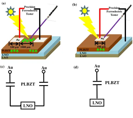
To study the ferroelectric and electrical characteristics, semi-transparent gold (Au) electrodes of
average thickness 40 nm in a square shape having a length 100 μm X 100 μm with a separation
of 1000 μm were deposited by using a shadow mask and performed electrical characterization as
shown in the schematic diagram (see Fig.3 (a &b)). Ferroelectric properties were measured at
room temperature using a Radiant ferroelectric tester. The current-voltage characteristics were
performed under illuminated of laser and white light using Keithley-236 source-meter at ambient
conditions.
Three conditions are employed to check ferroelectric polarization; i.e. dark (D), under
illumination of weak white light (W) with spectral range from 450 nm to 1200 nm and
light and laser source was nearly 60 mW/cm2 and 30 mW/cm2, respectively which illuminated at
the center of the semi-transparent electrode for the single capacitor and the center point between
two electrodes for the double capacitor. The nomenclatures 1D, 1W, 1L and 2D, 2W, 2L for
dark, illumination of white light, and illumination of laser for SC and DC, respectively.
3. Results and Discussion
3.1X-ray diffraction (XRD)
Figure. 1(a) shows the XRD patterns of highly oriented PLBZT thin films with an
average thickness about 150 nm grown on LNO (50 nm) coated LAO substrate. All peaks are
identified and mentioned in the fig. 1 (a), however (#) represents an alien peak of the substrate.
The XRD peak at 29.4° and hump XRD peak near 37° represent domain twining and impurities
of LAO substrate (not shown here). Sometime it develops due to imperfect growth, cutting and
polishing conditions of single crystal substrate. The LNO peak is very weak and also shadowed
by the highly intense (002) peak of LAO (marked in the Fig.1 (a)). The XRD patterns of as
received LAO substrate is given separately in supplementary information (Suppl. Fig.1). The
profilometer data confirming the film thickness (~150 nm) is also shown in supplementary
information (Suppl. Fig.2). The close view of PLBZT/LNO/LAO (002) peak with bulk PLBZT
XRD peaks is shown in figure 1 (b). The XRD patterns are shown in figure 1 (a) & (b) confirmed
phase purity and preferential orientation along (001) plane. A close view of (200) & (002) planes
of bulk PLBZT ceramics indicates that the PLBZT film possesses a large tensile strain along
(200) plane (in-plane) and compressive strain along (002) plane (out of plane) compared to the
bulk lattice. It occurs due to possible large lattice mismatch of bulk tetragonal PLBZT (lattice
substrate (a = 3.79 Å, c = 13.11 Å) [29]. To explore the effect of strain on the ferroelectric and
conductivity properties, the strain (ε) in the films due to lattice mismatch (or misfit) between
bulk and thin film was calculated using equation; ߝ =್ೠೖି
್ೠೖ × 100, where, ε is the lattice
strain, abulk is the lattice constant of the bulk, and afilm is the lattice constant of the film. If ε > 0,
films will experience plane tensile strain related to their bulk counterpart. Nearly 2.5%
in-plane tensile strain was observed in the film compared to bulk crystal structure. The magnitude
of strain is rather large which favors the condition for orientation of polarization along in-plane
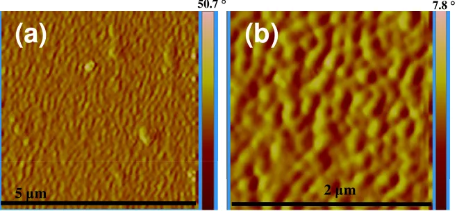
which predicts the possibility of large in-plane polarization. Figure 2 (a & b) shows surface
morphology of PLBZT thin film over an area of 5x5 μm and 2x2 μm on two different regions
that provide an average grain size of 10-25 nm and with average surface roughness of 1-3 nm. A
well dense wave nature of granular microstructure was seen in most of the investigated area.
3.2Schematic Illustration of circuit diagram
Figure 3(a) & (b) show a schematic circuit diagram which is used to measure the in-plane
and out-of-plane polarization and their enhancement under illumination of a light source. Figure
3(a) and (b) represent the DC and SC configuration with an equivalent electrical circuits Fig. 3(c)
and Fig. 3(d), respectively where the top square shape Au electrodes of 100 X 100 μm dimension
was fabricated using shadow mask with a separation of 1000 μm. The well saturated and concave
nature of polarization loops was observed under dark and illumination of light conditions.
3.3. Ferroelectric Properties
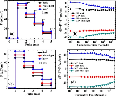
The ferroelectric polarization versus voltage (P-V) hysteresis loops and displacement currents
have been investigated to understand intrinsic polarization behavior of the highly oriented film
area between two electrodes (connected through bottom LNO electrode) was fabricated to probe
the polarization. P-V loops were symmetrical and saturated, and almost frequency independent
below 10 Hz probe frequency as can be seen from Fig. 4(a). A significant enhancement (nearly
100%) in ferroelectric polarization and displacement current were observed under illumination of
monochromatic light for DC configuration, whereas a small change (nearly 15 %) under
illumination in ferroelectric polarization (at 50 Hz) were observed in the case of SC
configuration. It indicates that a large amount of optically active charge carriers contribute
significantly for DC connected in series (due to the large active area) rather than SC
configuration under illumination. We have done polarization and PUND analysis for various
frequencies and pulse widths. The presented data is the best data where the film shows a
maximum change in polarization under illumination of light. The enhancement in polarization
under illumination of thin film heterostructure by an energy source may be due to the effective
contribution of electronic polarization and orientation of ionic polarization in the direction of
applied electric field. Matthew Dawber et. al. suggested that change in the spatial distribution of
2p electron orbitals of oxygen ions in perovskite octahedral may lead to the development of
electronic polarization [21] Here illumination of light changes the electronic weight of oxygen
2p orbitals which shifts opposite to the direction of central cations (Ti4+/Zr4+) responsible for
ionic polarization (Pion), resulting an additional electronic polarization (Pele) in the matrix in the
direction of ionic polarization [21]. It is also possible that under illumination of light, a large
number of electronic charge carriers jump from valance band to conduction band and developed
a shift current due to the asymmetry of the electronic band which may significantly affect the
3.4PUND analysis
A PUND (positive-up & negative-down) analysis has been carried out to check the
intrinsic polarization in both the configurations. We have used a 1ms (width) pulse signal with
15 V pulse amplitude to measure the polarization of DC connected through bottom electrode and
for a SC with out-of-plane configuration 10 ms (width) pulse signal with 10 V pulse amplitude.
These pulse widths and pulse amplitudes are optimized for both configurations to achieve
maximum control of polarization under illumination. Figure 5 (a,c) shows PUND plots for
various switchable and non-switchable polarization (remanent and saturation) of PLBZT film in
SC and DC modes of configuration. The net switchable polarization (dP) is as follows: dP = P* -
P^ = where P* = (switchable polarization + non-switchable polarization) and P^ =
(non-switchable polarization); dPr = P*r - P^r where P*r = (switchable remanent polarization +
non-switchable remanent polarization) and P^r = (non-switchable remanent polarization). The PUND
analysis indicates nearly 10% enhancement in switchable polarization compared to the 100%
enhancement in total polarization from the out-of-plane (DC) P-V hysteresis loops under
illumination of light. These results suggest that nearly 10% enhancement in intrinsic remanent
polarization under illumination, a similar magnitude of enhancement can be seen for the SC
configuration. The large difference between the switching and non-switching responses and
significant enhancement under illumination suggest a possible intrinsic polarization with and
without light and may be useful for developments of various logic states.
To measure the lifetime of the ferroelectric device under application of the external
electric field, a PUND based fatigue characteristics has been carried out on both configurations.
We have applied a train of a pulse having a pulse width 1 ms and amplitude 10 V across the
remanent polarization versus cumulative time under dark and illumination of white light is
displayed in Figure. 5(b,d). The fatigue results suggest nearly 30% degradation of remanent
polarization (2dP) after 105 cycles under white light illumination conditions for both the
configurations, however, nearly unchanged polarization under dark conditions. These results
suggest that the photo-generated charge carriers which relocate the electronic weight in the
lattice and saturate after a long period, however, the polarization under illumination are still
higher than the dark condition.
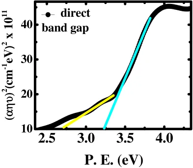
3.5 Band-gap calculation
Figure 6 shows the Tau plot of PLBZT thin films which indicate direct bandgap (~ 3.1
eV) where almost 75% transmission impede however another slope can be seen where almost
100% transmission stop. The last slope gives a direct band nearly 2.5 eV which may be due to
the presence of defects in the system. These values are less compared to the basic Ti-rich PZT
films (~ 3.5 eV).
3.6 Conduction mechanism in ferroelectric thin films
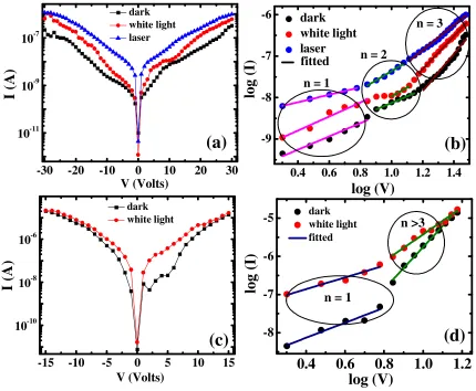
Figure 7 (a,c) shows the leakage current behavior in the dark and under illumination of an
external light source for SC and DC configurations, respectively. It is almost symmetrical in
nature under both positive and negative bias till ± 30 V and ± 15 V for DC and SC
configurations, respectively. The average dark current is about ~10-7 A at ±30 V and 10-5 A at ±
15 V for DC and SC, respectively. An order of higher current magnitude is observed in two
capacitors connected in the series configuration under illumination of white light and
monochromatic light. This enhancement in leakage current is due to optically active charge
modify the Fermi level and cross the Schottky electrode-ferroelectric barrier height. The
optically active charge carriers and cations trap the light and modify the surface charge layer,
redistribute the charge carriers across grain boundaries, and neutralization of depolarization field
at electrode-film interface. In DC configuration with large distance (1000 μm) between the
electrodes to avoid the contribution of photocurrent in intrinsic polarization, but at the same time
illumination of light also helps to develop electronic polarization which improves ionic
polarization and orient the in-plane polarization vector along the electric field. In general, the
photo-generated charge carriers annihilate within few micrometer distances, but some of them
hop to the nearest neighbor site and significantly contribute the electrical conduction.
All possible conduction mechanisms have been employed to understand the conduction
mechanism of PLBZT thin films, but none of them meet their theoretical criteria except trap
assisted space charge limited conduction (SCLC) mechanisms [31]. Figure 7 (b,d) shows the
linear fitting of the current-voltage data in three different voltage regions, low voltage region
follows Ohmic behavior, intermediate voltage meets the basic criteria of trap-assisted current
conduction process, and high voltage regions deep level trap assisted current conduction with an
exponent higher than 3. In the intermediate and high voltage regions, the injected charge carrier
increases very rapidly and quickly filled the trap centers and developed a condition of trap-free
conduction with a very narrow window of applied electric field. At low applied voltage, I-V
characteristics followed Ohmic current behavior because the densities of thermally generated
free carriers inside the films were larger than the injected charge carriers. When the internal field
is dominated by space charge (either from free or trapped carriers), the current (I) is expected to
follow a power-law dependence on voltage (I α Vn) [33]. I-V characteristics show that at a
bottom conductive electrode. Room temperature slope exponents (n) were found 1, 2 and 3
which represent initial Ohmic conduction, intermediate trap-assisted conduction and high voltage
deep level trap-free conduction, respectively which suggest that SCLC conduction is likely to be
the dominant leakage mechanism.
The present investigation was intended to check the control of polarization by various
weak light sources to develop multistate NV-FeRAM logic elements. In this regards, we have
characterized two basic configurations of out of plane capacitor-type device. First, we probed a
conventional single capacitor (SC) with semi-transparent top Au electrode and conducting LNO
bottom electrode. In this particular configuration, the device provides nearly 12% enhancements
in polarization under illumination of a weak light source. To improve the effect of light on
polarization, we further studied an alternative device structure where two single capacitors
situated nearby were connected through bottom electrode in series. It was expected that the
second configuration should provide significant enhancement in polarization under illumination
of a weak light source since this particular configuration take advantage of the surface
polarization as well as out of plane polarization and its maximum interaction with light (surface
area). As expected nearly 100% enhancement in polarization was observed for DC configuration
for a weak light source. The DC configuration will also provide an extra degree of freedom for
miniaturization of an optically active device for future microelectronics.
4. Conclusions:
We have investigated two out-of-plane configurations of PLBZT device; (i) the DC
connected through conducting bottom LNO electrode and (ii) a SC with top Au electrode and
possible ferroelectric polarization-based logic elements. A detailed investigation of
well-saturated hysteresis loops, enhancement of polarization under illumination of a light source,
PUND based switchable polarization, and displacement current suggests the intrinsic nature of
polarization and displacement current and its enhancement under illumination of light. The
substitution of optically active cations significantly reduced the direct bandgap (~ 3.1 eV)
compared to the basic Ti-rich PZT films. Almost thirty percent polarization fatigue was observed
for a large number of test cycles under illumination of light. However, negligible reduction in
polarization was seen in dark conditions. The current conduction process meets the criteria of
space charge limited mechanism which becomes trap-free at high applied voltage. These results
may help the engineers to design out-of-plane ferroelectric memory cell with electrically write
and optically read process.
Acknowledgment
Ashok Kumar acknowledges the CSIR-NPL, India project PSC-0111. Hitesh Borkar would like
to acknowledge the UGC-SRF to provide fellowship to carry out the Ph.D program. Authors
sincerely thank the Director, NPL, Dr. Ranjana Mehrotra and Dr. Sanjay Yadav for their constant
Figure captions
Fig. 1 (a) X-ray diffraction patterns of PLBZT/LNO/LAO epitaxial thin film over a wide range
of Bragg's angle. Fig. 1(b) shows the close view of (002) PLBZT film plane and compared with
lattice plane of bulk PLBZT ceramics in the same Braggs angle range.
Fig. 2 Surface topography image of PLBZT thin film over an area of (a) 5μm x 5μm and (b)
2μm x 2μm at two different places on the surface.
Fig.3 (a) shows a schematic illustration of the testbed device structure for two out-of-plane
capacitors i.e. double capacitor (DC) connected through bottom electrode, (b) single capacitor
(SC) device structure, (c) circuit diagram for DC in series connection and (d) circuit diagram of
SC for out-of-plane configuration.
Fig.4 (a) illustrates ferroelectric polarization and (b) switching of displacement under three
different conditions i.e. 2D, 2W, & 2L for DC at 10 Hz, respectively. Fig. 3 (c) and (d) illustrate
ferroelectric polarization and switching of displacement current under three different conditions
i.e. 1D, 1W, & 1L for SC at 50 Hz, respectively.
Fig.5 (a) & (b) show the PUND data and fatigue characteristics of DC that utilized a pulse signal
of width 1 ms and amplitude 15 V for PUND and 10 V for fatigue, respectively. Fig 5 (c) & (d)
show the PUND data and fatigue characteristics of SC that utilized a pulse signal of width 10 ms
Fig.6 Illustrates the Tau plot of PLBZT thin film without bottom electrode to calculate the
bandgap of the system.
Fig.7 (a) & (b) show the leakage current (I) as a function of applied voltage (V) and linear fitting
of I-V characteristics in log-log scale to check the suitability of SCLC mechanism for DC mode
under 2D, 2W, and 2L, respectively. Fig. 6 (c) and (d) show the leakage current (I) as a function
of applied voltage (V) and its linear fitting for SC mode under 1D and 1W condition,
(b)
40
45
50
L A O (0 0 2 ) L N O (0 0 2 ) (2 0 1 ) (2 1 0 ) (1 0 2 ) (0 0 2 )
In
te
n
si
ty
(
a
rb
.u
n
it
)
2θ
2θ
2θ
2θ
((((degree)
B u lk P L B Z T * (2 0 0 ) P L B Z T (0 0 2 ) Film
20
40
60
80
L A O (0 0 3 ) P L B Z T (0 0 3 ) P L B Z T (0 0 1 ) L N O (0 0 2 ) P L B Z T (0 0 2 ) L A O (0 0 2 ) #
In
te
n
si
ty
(
a
rb
.u
n
it
)
2θ
2θ
2θ
2θ
(degree
)#
Figure 1
Figure 2
5 μm 2 μm
7.8 °
50.7 °
Figure 3
(a)
LNO
Au
Au
PLBZT
100 μm
LAO PLBZT
LNO
Precision Ferroelectric
Tester
Au
LNO
Au
PLBZT
(b)
(c) (d)
LAO
PLBZT
LNO
Precision Ferroelectric
Tester
100 μm 1000 μm
-10 -5 0 5 10 -30 -20 -10 0 10 20 J D ( µµµµ A /c m 2 ) V (Volts) dark white light laser 50 Hz
-10 -5 0 5 10
-60 -40 -20 0 20 40 60 P ( µµµµ C /c m 2 ) V (Volts) 50 Hz dark white light laser
-15 -10 -5 0 5 10 15
-4 -2 0 2 4 6 J D ( µµµµ A /c m 2 ) dark white light laser 10 Hz V (Volts)
(b)
(d)
(c)
-15 -10 -5 0 5 10 15
Figure 4
Figure 5
100 101 102 103 104 105
-40 -30 -20 -10 0 10 20 30 40
Cumulative Time (Seconds)
2dP: dark -2dP: dark 2dP: white light -2dP: white light
d P = P * -P ^ ( µµµµ c/ cm 2 )
100 101 102 103 104 105 -20
-10 0 10 20
Cumulative Time (Seconds)
d P = P * -P ^ ( µµµµ c/ cm 2 ) 2dP: dark -2dP: dark 2dP: white light -2dP: white light
(d)
(c)
(b)
1 2 3 4 5
0 20 40 60 80 10 ms Pulse (ms) P ( µµµµ C /c m 2 ) dark white light laser
0 1 2 3 4 5
Figure 6
2.5
3.0
3.5
4.0
10
20
30
40
P. E. (eV)
(α
η
υ
)
(α
η
υ
)
(α
η
υ
)
(α
η
υ
)
2
(
cm
-1
eV
)
2
x
1
0
1
1
direct
Figure 7
0.4
0.6
0.8
1.0
1.2
-8 -7 -6 -5
lo
g
(
I)
log (V)
n >3n = 1
dark white light fitted
0.4 0.6 0.8 1.0 1.2 1.4 -9
-8 -7 -6
fitted
n = 3
n = 2
n = 1 dark white light laser
log (V)
lo
g
(
I)
-30 -20 -10 0 10 20 30 10-11 10-9 10-7 V (Volts) dark white light laser
I
(A
)
References:
[1] Dawber M., Rabe K. M., Scott J. F., 2005 Rev. Mod. Phys.77, 1083.
[2] Catalan G., Seidel J., Ramesh R., Scott J. F., 2012, Rev. Mod. Phys.84, 119.
[3] MatzenS., NesterovO., RispensG., HeuverJ. A., BiegalskiM., ChristenH. M., Noheda B., 2014, Nature Communications 5, 4415.
[4] Tsymbal E. Y., Gruverman A., Garcia V., Bibes M., Barthelemy A., 2012 MRS Bull.37, 138.
[5] Fu H., Bellaiche L., 2003 Phys. Rev. Lett.91, 257601.
[6] Schilling A., ByrneD., Catalan G., Webber K. G., GenenkoY. A., Wu G. S., Scott J. F.and GreggJ. M., 2009, Nano Lett.9, 3359.
[7] Balke N., WinchesterB., RenW., ChuY. H., MorozovskaA. N., EliseevE. A., Huijben M., VasudevanR. K., MaksymovychP., BritsonJ., et. al, 2012 Nat. Phys.8, 81.
[8] Yang S. Y., Seidel J., Byrnes S. J., Shafer P., Yang C. H., Rossell M. D., Yu P., Chu Y. H., Scott J. F., Ager J. W., III, Martin L. W., Ramesh R., 2010Nature Nanotechnology5, 143.
[9] Uchino K., 2000 Ferroelectric Devices, Marcel Dekker, New York.
[10] Lines M. E. and Glass A. M., 1977 Principles and Applications of Ferroelectrics and Related Materials, Oxford University, New York.
[11] Scott J. F., 2007, Science315, 954.
[12] Kholkin A. L. and Setter N., 1997 Appl. Phys. Lett., 71, 2854.
[13] Polkawich R. L.and Trolier-McKinstry S., 2000 J. Mater. Res.,15, 2505.
[14] Kholkin A., Boiarkine O., and Setter N., 1998 Appl. Phys. Lett.72, 130.
[15] Zubko P. and Triscone J. M., 2009 Nature, 460, 45.
[16] Wadhawan V. K., Introduction to Ferroic Materials, Gordon and Breach Science Publishers, Amsterdam (2000).
[17] Alexe M. and Hesse D., 2011 Nat. Commun.2, 256.
[18] Choi T., Lee S., Choi Y. J., Kiryukhin V. and Cheong S. W., 2009, Science, 324, 63.
[19] Kumar A., Borkar H., Rao V., Tomar M., Gupta V., Multi-States Nonvolatile Opto-Ferroelectric Memory 2016, Indian patentNo #: 201611001338.
[20] Hu W. J., Wang Z., Yu W., Wu T., Nature Comm.7, 10808 (2016).
[21] Dawber M. 2012 Physics5, 63.
[22] Land C. E. and Smith W. D., 1973 Appl. Phys. Lett., 23, 57.
[23]Maldonado R., Fraser D. B., and Meitzler A. H., 1975 In Advance in image Pickup and Display, edited by B. Kazan Academic, New York, 65, 168.
[24] Borkar H., Tomar M., Gupta V., Scott J. F., Kumar A., 2015 Appl. Phys. Lett., 107(12),
122904.
[25] Kundys B., Viret M., Colson D., and Kundys D. O., 2010 Nat. Mater.9, 803.
[26] Polkawich R. L. and Trolier-McKinstry S., 2000 J. Mater. Res. 15, 2505.
[28] Borkar H., Rao V., Tomar M., Gupta V., Scott J. F., Kumar A., 2017 RSC Advances
7,12842 .
[29] Luo X. and Wang B., 2008 J. Appl. Phys.104, 073518.
[30] Young S. M., Rappe A. M., 2012, Phys. Rev. Lett.109, 116601.