TCAD device simulation of novel test structures for
determining the lifetime in solar cells
Javid Aliyev, Ray Hueting, Rufat Alizada, Lis Nanver
Department of Semiconductor Components, University of Twente, Enschede, The
Netherlands
(emails: [email protected], [email protected])
Abstract—In this work a new device test structure for determining the charge carrier lifetime in solar cells is investigated using device simulations. This structure comprises apnpphototransistor structure, which allows to determine the recombination or (effective) lifetime at the surface or in the shallow junction of the transistor. Several separate current components can be investigated, including that component solely determined by recombination at the surface, not possible in a standard diode or solar cell. Yet, the heart of this transistor basically imitates the solar cell. Investigating the current characteristics of the given structures and calculating the lifetime gives a clear explanation of the recombination process in solar cells, which is one of the main factors influencing the efficiency of solar cells.
By examining the current density values calculated and simulated with different methods, the test structure is proven to be valid for the carrier lifetime investigation. A different outcome between a cylindrical and a 2D structure is observed, which can be attributed to base current spreading. The results indicate that a less uniform current flow is obtained for a wide cylindrical structure making this structure less suitable for lifetime extraction. The re-lation between current density and effective recombination along with the calculations of the sheet resistance are also presented.
This work is important for improving the solar cell efficiency.
Index Terms—Solar cell, carrier lifetime, surface recom-bination, phototransistor, base current, electron concentra-tion, current density, TCAD.
I. INTRODUCTION
T
HE worldwide demand for energy forces more and more people to rely on renewable energy sources rather than conventional ones. Solar cells appear to play a big role in satisfying today’s grow-ing energy demand in an environmentally benign way. But, for implementing those in a mass scale, further cost reduction is essential [1]. To reduce thecosts many approaches have been considered, some of which affect the conversion efficiency of solar cells.
Surface recombination is one of the factors that influence efficiency of cells. Reducing the surface recombination leads to a longer carrier lifetime. The lifetime is a measure of how long a carrier is likely to stay around before recombining and is one of the most important parameters for the characterization of power electronic devices and photovoltaic solar cells. In particular, determining the lifetime plays an important role in optimization of solar cell per-formance. Therefore, a clear understanding of how many and where carriers are recombining is crucial for solar cell efficiency. However, determining the value and location of the (effective) lifetime in a solar cell, which is basically a diode, remains to be an issue. Surface recombination and lifetime in silicon devices have been studied and different lifetime extraction approaches were proposed [2], [3], [4]. However, the effect of carrier trapping on lifetime measurements should be taken into account. When traps are present, carriers tend to get trapped, but they do not recombine. Therefore, the measured apparent lifetime does not represent the actual recombination lifetime [5], and hence cause significant problems with the measurements [6].
test structures [9] can be optimized further by fine tuning several device parameters.
In this paper these test structures will be ex-plained. The approach is to adopt the device simula-tion software to investigate the effect of lifetime or surface recombination on the device performance, thus, on efficiency of solar cells. The paper will conclude on whether this test structure is suitable for carrier lifetime investigation.
II. TEST STRUCTURE
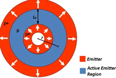
Figure 1 shows the schematic cross-section of the pnp phototransistor. We investigate both a 2D and a cylindrical structure with a constant radius
r =68.5 µm to the center of the active emitter
[image:2.612.343.534.59.187.2]layer, that is rotated around the indicated dashed line. The structure consists of two p+-type emitters and a shallow p-type region, i.e. the active emitter region, in between. This region has been varied to investigate electron current density, using different methods elaborated in section III.
Fig. 1: Cross section of the test structures: (a) with electrode and (b) oxide layer. E and B indicate the emitter and base contact regions respectively.
Figure 1a illustrates a structure with an electrode on top of the active emitter region. By using an artificial electrode bulk and interfacial recombina-tion effects are included in a single parameter called (effective) surface recombination velocity. Figure 1b shows a similar structure with an oxide layer instead of an artificial contact, which is more realistic and can be compared to real lifetime measurements. The purpose of using the first structure is to at-tract more electrons to the active emitter region
Fig. 2: The basic structure of the totalpregion.
TABLE I: Test parameters
Base contact width 2µm Emitter contact width 1µm
Substrate thickness 200µm Base thickness 1µm n-type base doping 2e16 cm−3 p-type substrate doping 1e15 cm−3 Base doping implant 2.5e20 cm−3 Emitter doping implant 1.5e20 cm−3 Junction depth 0.0022µm
Temperature 300 K
and, hence, to better illustrate the electron current density extraction method explained in section III. The highlighted region in Figure 1a shows the part that imitates a diode, thus a solar cell. By analysing this structure, it is possible to investigate several separate current components and determine the carrier lifetime, which is not possible in real-life measurements of a standard diode or solar cell.
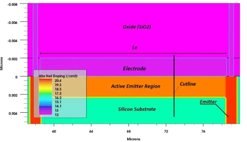
Figure 3 shows the zoomed-in device structure with the electrode with a surface recombination ve-locity of 102 cm/s constructed using Silvaco TCAD and plotted with Tonyplot. The length of the active emitter region, as well as many other parameters, such as device geometry, temperature, doping and surface recombination velocity (or lifetime), are included as variables. A variation of the electrode and oxide on top of the p layer has also been done. The doping profiles, like all other fixed parameters, are assumed to be uniform (see Table I).
[image:2.612.52.298.367.567.2]Fig. 3: Cross section of the test structure plotted with Tonyplot
III. METHOD
A. Electron current at interface
It is important to notice that the base current consists of two components: In and Ip, where In
is the electron current component from the base to emitter and Ip - the hole component from the
emitter to base. Because of the special structure of the phototransistor, the electron base current itself also consists of two components: In1 andIn2, where
In1 is the electron component from base to emitter and In2 - to the active shallow emitter layer. Thus,
Ib=Ip+In=Ip+In1+In2 (1)
whereIn2=Jn2·A, withA- area of the active emitter
region.
In this work the second electron current com-ponent will be investigated, since this comcom-ponent is determined by the surface recombination. It is important to mention that surface recombination is a measure of the lifetime, as addressed in the appendix. To disentangle this component from the whole base current, the length of the active layer (Le) is varied (from 4 to 44µm). By varying this
length, base current values corresponding to dif-ferent Le values can be determined. Further, it is shown that subtracting these Ib values leaves only
In2component. From4Ib vs4Legraph the electron
current density can be calculated using:
Jn= 4Ib
4A =
4Ib
2πr· 4Le
(2)
where r is the fixed radius of the emitter ring and
Le is the active emitter layer length.
To show that calculated Jn indeed corresponds to the second component of the electron current density, Jn2 is extracted using the cutline function
of Tonyplot (see Figure 3). A vertical line crossing the active emitter layer is used to look inside of the device, allowing direct determination of Jn2.
Another method of obtaining this value is from 1D electron distribution inside the layer using the following formula [8]:
Jn2=qDn·
(n2−n1)
d ≈qDn· n2
d (3)
where,
Dn= µnkBT
q (4)
with µn - mobility of electrons, kB - Boltzmann’s
constant, T - temperature, Dn - diffusion constant
and q - the elementary charge,d - diffusion length. The excess minority concentration n2 at the base side of the active emitter layer has its maximum. Diffusion takes place resulting in an excess concen-tration smaller than n2 [8]. The Silvaco software
makes it possible to examine the distribution. Same results obtained from different methods indicate that studying the active layer and inves-tigating electron current component determined by the surface recombination is possible using the test device.
Alternatively, from electrons diffusing through a p-type region with an electrode [13], [14] or some non-ideal interface on top (see Figure 6), the relation between the electron current density and effective recombination velocity can be derived (see Appendix):
Jn= q·Seff(n1−n0)≈q·Seff·n1, (5)
where q is electron charge, Seff is the effective recombination velocity, n0 is the equilibrium
con-centration and n1 is the concentration at the surface
of the artificial contact or interface.
B. Sheet Resistance
of the resulting linear I-V curve the resistance can be determined. In transistors and other electronic devices, the contacts are part of the device, and con-tribute to the contact resistance. So, the simulated resistance consists of two components:
Rm=Rs+2Rc, (6)
where Rs is the semiconductor resistance and Rc is the contact resistance.
The cylindrical ring structure has a fixed perime-ter, therefore only two variables are important for the sheet resistance extraction: the measured resis-tance Rm of each structure and the active emitter region lengthLe. The contact resistance can be
elim-inated, by measuring the resistance between two emitter contacts for a set of different active emitter lengths. Resistance values Rm are subtracted and plotted against corresponding length differences. Thus, only the first component of Eq. (6) is left. The slope of the resulting4Rm vs4Le graph gives
a number corresponding to the value of Rsh/w [8],
where Rsh is the sheet resistance and w - width of the layer. From this slope the sheet resistance can be calculated.
In [9] three methods of performing the differential extraction of Rsh, each with an increasing degree of complexity and validity, are described, where the first one is the aforementioned method. The second method takes the radial spreading of the current into account, which is important for large 4Le values.
Hence,
Rmj−Rmi=Rsh·αijedge (7)
and
αijedge= 1
2πln[
r+0.5·Lij
r−0.5·Lij], (8)
where indexes i=1, ...,n and j =1, ...,n refer to each specific test structure (with j>i) and Lij =
Lj−Li=4Le.
The third method is applied when the length of subtracted regions become so large, that the radial spreading through these regions cannot be neglected. An accurate differential relationship can be established by subtracting the region of Li at the center of Lj rather than at the edges [9]. Thus,
Rmj−Rmi=Rsh·αijedge (9)
and
αijedge= 1
2πln[
(r−0.5·Li)(r+0.5·Lj)
(r+0.5·Li)(r−0.5·Lj)]. (10)
To show the validity of the calculated value, the sheet resistance can also be derived with [8]:
Rsh=ρ
d =
1
qR∞
0 µp(x)·N(x)Adr
≈ 1
µpqNAd
(11)
where N is the doping concentration of the active emitter layer. The value ofµpis directly taken from
the simulations using the cutline function.
C. Ideality factor
The ideality factor of a diode is a measure of how closely the diode follows the ideal diode equation. The ideal diode equation assumes that all the recom-bination occurs via band to band or recomrecom-bination via traps in the bulk areas (i.e. quasi-neutral areas) from the device. Using that assumption, the deriva-tion produces the ideal diode equaderiva-tion with ideality factor n of 1 [10]:
I=I0·(e V
n·uT −1) (12)
whereIis the current through the diode,V - voltage across the diode, I0 - dark saturation current and n
- ideality factor. For relatively high forward voltage values the -1 term can be neglected.
However, recombination does occur in other ways and in other areas of the device, e.g. recombination inside the depletion region (SRH recombination [8]). This type of recombination produces an ideal-ity factor that deviates from the ideal case. In order to calculate the ideality factor, log of both sides of Eq. (12) can be taken:
ln(I) =ln(I0) +
1
uTln(10)·V (13)
When plotting the natural log of the current against the voltage, the slope gives uTln(10)/n and the intercept gives ln(I0). Thus, the ideality factor
can be found from the slope (for 0.4 V) (see Figure 4):
n= (
∂logI ∂V )
−1
uTln(10) =
(1.66/0.1)−1
IV. RESULTS
A. Surface recombination
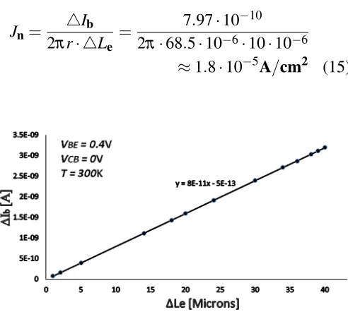
Figure 4 illustrates the Gummel plot taken from simulations of the structure (for Le=44µm). Base
[image:5.612.319.561.58.182.2]current values for each active emitter length at 0.4V were derived, and subtracted current values were plotted against the length differences (see Figure 5).
Fig. 4: Gummel plot forLe=44µm obtained from simulations
Using Eq. (2) for a cylindrical structure Jn can be calculated:
Jn=
4Ib
2πr· 4Le
= 7.97·10
−10
[image:5.612.50.306.175.332.2]2π·68.5·10−6·10·10−6 ≈1.8·10−5A/cm2 (15)
Fig. 5:4Ibplotted against subtracted active emitter layer length (4Le)
extracted from cylindrical structures
Figure 6 illustrates the electron concentration and
Jn of the active emitter layer. The value of Jn was
found to be around 1.6·10−5A/cm2, which is very close to the value calculated in Eq. (15).
[image:5.612.52.298.390.611.2]From Figure 6 it can be seen that the minority carriers show a near linear decrease towards the electrode. In case of a short distance between the
Fig. 6: Electron concentration andJnsimulated using cutline function
electrode and the edge of the depletion layer expo-nential decay, which is inherent to the recombina-tion process, can be approximated by a linear decay. However, due to some bulk recombination inside the layer simulated line is not perfectly linear.
By substituting values of electron concentrations into Eq. (3), the value of electron current density was derived:
Jn ≈qDn·n2
d =
=0.4975·1.602·10−19· 2.8438·10 8
4.56·10−6−3.36·10−6 ≈1.88·10−5A/cm2 (16)
All three methods gave similar results, meaning that the test structures are suitable for active emitter region analysis.
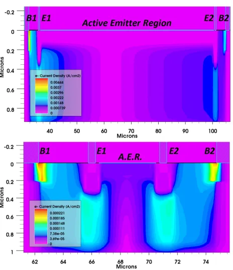
As a next step, in order to see the relation with the lifetime, the surface recombination in the active emitter area was varied. The electron current density was simulated for the cylindrical structure, and the results showed that Jn is decreasing horizontally from emitter 1 to emitter 2 (see Figure 9). Therefore, with increasing active emitter region length, the horizontal variation of Jn also increased (see Table
II). Hence, there is a non-uniform current flow for large cylindrical structures. Figure 7 shows the electron current density contour of the simulated structure for two different Le values. This figure
also indicates that for large Le the current flowing
from base 1 to emitter 1 is higher than the current flowing from base 2 to emitter 2. The reason of that is the radial spreading of the current in cylindrical structures, even at low injection.
Fig. 7: Electron current density contour plot in a cylindrical structure for Le=64µm andLe=4µm
TABLE II: Difference in electron current density for different active emitter region lengths (see Figure 9)
Le[µm] J1[A/cm2] J2[A/cm2] 4 3.016·10−5 2.89·10−5 10 3.12·10−5 2.7826·10−5 20 3.3556·10−5 2.6259·10−5 24 3.4537·10−5 2.5707·10−5 34 3.7249·10−5 2.4366·10−5 44 4.0446·10−5 2.32·10−5 64 4.87·10−5 2.11·10−5
Jn=
4Ib
2πr· 4Le
= 1.25·10
−10
2π·68.5·10−6·10−6
≈2.9·10−5A/cm2 (17)
For smallLethe horizontal component of electron current density can be assumed to be constant, and the result of Eq. (17) matches with the simulation results (for Seff = 104cm/s). However, for large
Le the variation in current density becomes more significant (see Table II) and derived Jn cannot be compared to simulation results. For confirmation, the structure was changed to 2D, and here a constant
Jn component was observed irrespective of the Le
[image:6.612.313.552.229.361.2]value. This implies that the current flow is strongly affected by the curvature of the cylindrical struc-tures, unlike in 2D structures.
Fig. 8: Electron current density simulated with horizontal cutline through active emitter region
Fig. 9: Electron current density simulated with horizontal cutline through active emitter region forLe=20µm
For an additional check for the 2D structure, Jn
for different surface recombination values was simu-lated (see Table III). Figure 10 illustrates the Gum-mel plot of the base currents plotted for different surface recombination velocity values [12], showing that the increase inSeff provokes the increase of the base current. This behaviour is in agreement with Eq. (5).
Fig. 10: Gummel plot of the base currents for different surface recombination velocities
[image:6.612.60.292.381.575.2] [image:6.612.317.558.539.684.2]and electron concentration into Eq. (5):
Jn=q·Seff(n1−n0) =
1.602·10−19·105·(8.6517·108− 10 22
7.12·1019) ≈1.4·10−5A/cm2 (18)
The calculated value (forSeff=105cm/s) matched with the simulated one (see Table III).
As in case of the cylindrical structure, base cur-rent values for each active emitter length at 0.4V for
Seff=105cm/s were derived, and subtracted current values were plotted against the length differences (see Figure 11). Since the simulated structure is here 2D, following formula was used to calculate electron current density:
Jn = 4Ib 4Le
[image:7.612.388.488.75.131.2]≈1.43·10−5A/cm2 (19)
Fig. 11:4Ibplotted against subtracted active emitter layer length extarcted
from 2D structures (forSeff=105cm/s)
So, Eqs. (18) and (19), as well as simulation results (see Table III), gave similar results, meaning that the effect of added surface recombination is correct. This experiment has been done for different surface recombination values. However, for much lower values (e.g. Seff=102cm/s) derived electron current density did not match with the results from Table III. The reason for that could be that the electron current flowing from base to emitter is much higher than the current flowing to the active emitter region, and for very low surface recombina-tion values Jn becomes negligibly low. Since then
surface recombination is less important, this is no issue.
These experiments imply that indeed lifetime in solar cells can be extracted using this test structure.
TABLE III: Relation between simulated electron current density and surface recombination
Jn[A/cm2] Seff[cm/s] 1.5·10−8 102 1.49·10−7 103 1.48·10−6 104 1.39·10−5 105
TABLE IV: Sheet resistance derived with three different methods reported in [9]
Lij [µm] Rsh(M1) [Ω] Rsh(M2) [Ω] Rsh(M3) [Ω]
1 173.5184 173.5147 173.326
2 173.4375 173.4315 173.2031
4 173.8955 173.8521 173.2928
6 173.6621 173.6247 173.2522
16 183.6515 182.7897 173.367
20 182.5151 181.2219 173.3685 24 178.4732 176.6424 173.3502
56 190.0457 178.9422 173.402
59 189.2097 176.8695 173.377
B. Sheet Resistance
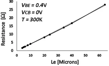
[image:7.612.65.284.298.491.2]To find the sheet resistance, 0.4V was applied on emitters of the cylindrical structures with different active emitter layer lengths. From the I-V curves resistance values were derived (see Figure 12).
Fig. 12: Simulated resistance values plotted against active emitter layer length for cylindrical structure
As explained in section III, three methods of deriving sheet resistance were used. Table IV sum-marizes sheet resistance values derived for different subtracted active emitter region length values. Ide-ally, different subtracted length values with the cor-responding resistance values from Figure 12 should give the same sheet resistance. From Table IV, it is clearly seen that the sheet resistance value obtained from the first and second methods fluctuate, whereas the third method gives a constant number, meaning that it is more accurate.
[image:7.612.326.551.405.541.2]Rsh=Rmj−Rmi
αijedge
= Rmj−Rmi
1 2πln[
(r−0.5·Li)(r+0.5·Lj)
(r+0.5·Li)(r−0.5·Lj)] ≈173Ω/2 (20)
To check the validity of the sheet resistance value calculated using the third method, Eq. (11) was used:
Rsh= ρ
d =
1
µnqNd
=
1
30·1.602·10−19·1021·1.2·10−6
≈173Ω/2, (21)
where the value of the electron mobility µn was
taken from simulations using the cutline function. As Eqs. (20) and (21) gave the same result, it can be concluded that the surface channel sheet resistance of the structure with an oxide layer on top of the active emitter layer was derived correctly. Unfortunately, actual sheet resistance measure-ments of the structure with an oxide layer on top were not available. Therefore, the values calculated from simulations could not be compared to the measured data.
V. CONCLUSION
In this paper, dedicated phototransistor test struc-tures, all imitating a solar cell, were simulated. By varying the length of the active emitter layer, the actual value of the electron current density was found. Several methods were used to show the validity of this value. In turn, from the electron current density the surface recombination or lifetime can be extracted, showing that these structures are suitable for analysing the efficiency of solar cells. Difference between the cylindrical and 2D structures was observed, as the horizontal component of the electron current density at the active emitter region of the cylindrical structure showed a non-uniform behaviour due to radial spreading. Therefore, further comparison of different methods of extraction of the electron current density value for cylindrical structure with large Le was not possible. For this 2D structures are advised.
In addition, the differential measurement tech-nique using the test structure has been demonstrated
to be a technique of accurately determining the surface channel sheet resistance. This allows a direct comparison with the sheet resistance measured in the lab.
For future research it is suggested to use more realistic profiles of the structure to be able to com-pare simulation results with the actual measurement results.
VI. APPENDIX
First, an artificial contact is considered on top of the active emitter region. In this way possible bulk and/or interfacial recombination effects are incorporated in a single parameter called (effective) surface recombination velocity Seff [13], [14].
From the change in carrier density due to the dif-ference between the incoming and outgoing flux of carriers the following continuity equation is derived [15]:
1
q·
∂Jn ∂x =
n(x)
τ (22)
where
n=n1·ex−Lw (23)
withw- artificial contact thickness andL- diffusion length. Hence,
Jn=q·
Z w
0
n1
τ ·e x−w
L dx (24)
Assuming wL:
Jn =
qn1L
τ =q
r
Dn
τ ·n1≡q·Seff(n1−n0) (25)
Therefore,
Seff≡
r
Dn
τ (26)
However, in case of an ultra-thin interfacial layer in which the minority concentration drops to equi-librium value n0 (e.g. oxide layer), the derivation
changes. Assuming 0 Lδ w, where δ is
the thickness of the interface (e.g. silicon-dioxide interface):
Jn≈ lim
δ→0
qδ
τ(
n1−n0
2 +n0)≈δlim→0
qδ
2τn1 (27)
Thus,
Seff≡ lim
δ→0 δ
2τ (28)
REFERENCES
[1] Islam, K., and Nayfeh, A. ”Simulation of a-Si/c-GaAs/c-Si Heterojunction Solar Cells.” Computer Modeling and Simulation (EMS), 2012 Sixth UKSim/AMSS European Symposium : 466-470.
[2] Neugroschel, A. ”Determination of lifetimes and recombination currents in pn junction solar cells, diodes, and transistors.” Electron Devices, IEEE Transactions on 28.1 (1981): 108-115. [3] Gonzalez, F. N, and Neugroschel, A. ”Measurement of diffusion
length, lifetime, and surface recombination velocity in thin semiconductor layers.” Electron Devices, IEEE Transactions on 31.4 (1984): 413-416.
[4] Lederhandler, SRj, and Giacoletto, LJ. ”Measurement of mi-nority carrier lifetime and surface effects in junction devices.” Proceedings of the IRE 43.4 (1955): 477-483.
[5] Macdonald, Daniel, Ronald A Sinton, and Andrs Cuevas. ”On the use of a bias-light correction for trapping effects in photoconductance-based lifetime measurements of silicon.” Journal of Applied Physics 89.5 (2001): 2772-2778.
[6] Fahrenbruch, A. L, and Bube, R. H. Fundamentals of Solar Cells: Photovoltaic Solar Energy Conversion. New York: Academic Press, 1983.
[7] Atlas TCAD process and device simulation software, Silvaco, Inc., Available: http://www.silvaco.com/
[8] Sze, S. M, and Ng. K.K. Physics of semiconductor devices. John wiley and sons, 2007.
[9] Evseev, SB, Nanver, LK and Milosavljevi, S. ”Ring-gate MOS-FET test structures for measuring surface-charge-layer sheet resistance on high-resistivity-silicon substrates.” Proc. 19th IEEE Int. Conf. on Microelectronic Test Structures (ICMTS) 6 Mar. 2006: 3-8.
[10] McIntosh K. R. and Honsberg, C. B., The Influence of Edge Recombination on a Solar Cells IV Curve, 16th European Photovoltaic Solar Energy Conference. 2000.
[11] Schroder, D. K. Semiconductor material and device character-ization. John Wiley and Sons, 2006.
[12] Touboul A. et al. (1998). Proceedings of the 28th European Solid-State Devices. Bordeaux, France
[13] De Graaff, HC, Slotboom, JW. and Schmitz, A. ”The emitter efficiency of bipolar transistors: Theory and experiments.” Solid-State Electronics 20.6 (1977): 515-521.
[14] Post, I. R.C, Ashburn, P. and Wolstenholme, G.R. ”Polysilicon emitters for bipolar transistors: a review and re-evaluation of theory and experiment.” Electron Devices, IEEE Transactions on 39.7 (1992): 1717-1731.