WINCHESTER
TECHNICAL MANUAL
11
&
23MB VERSIONS
AVAILABLE IN 5500, 5600, 5615, 5700, 5011, 5013, & 5015
1. 2. 3. 4. 5. CO}'7ENTS
GENERAL
...
FEATURES
...
Compact Size
... . ...
Inexpensive ••.••••••
High Reliability •••••••••••••••.•••••••••.••. 2.1 2.2 2.3 2.4 2.5 2.6
Preventive Maintenance ..••...•.••••.••..•...•....
DC Pover Supply . . . .
Physical Dimensions •••.•.••.•••••••••••.••...•
2.7 Vertical or Horizontal Installation ••••••••.•.
2.8 Lo~ Power Consu~ption
2.9 Lo~ Noise 2.10 Low Vibration
SPECIFICATIONS 3.1 3.2 3.3 ~.4 3.5 3.6 Performance Reliability
Error Rate
Positioning Time
Start and Stop Time .••.••..••
Environmental Conditions
.
....
STRUCTt'TRE .•••••••••••••••••••••.•.••••.•.••••••••.•• .o • •
4.1 4.2
External Size
Unit Structure
INSTALLATION
5.1 5.2 5.3
Locker Installation
Service Areas
6.
7.
8.
CABLE CONNECTION
.
... .
6.1 6.2 6.3 6.4 6.5 6.6
Unit Connectors
...
Cable ~onnector Specifications ••••••••••••••••••••••• Single Connection
...
Connecting Multiple Units •••••••••••••••••••••••.•.••
...
Driver/Receiver
DC grounding
...
INTERFACE
7.1 7.2
7.3
Signal Lines
Input Signals
Output Signals
...
7.4 Timing Specifjcations
7.4.1 Seek timing
"J .4 • 2 Read /lI .. ri,te data timing •••••••••••••.•••••••••••••
7.5 Formats •.•••••••.•••.
7.5.1 Track format
7.5.2 Read/Write timing
7.6 Connector Positions
.
.
.
. . .
.
.
.
.
.
.
.
.
.
.
.
.
.
.
.
.
. . .
.
.
,
.
...
7 • 7 Power Supply Input Connector •••••.••.••••••.••••••••••
POWER SUPPLY COh~ITIONS
8.1 8.2 8.3 8.4 8.5 8.6
Input Voltage and Permissible Input Voltage
Variation ... .
Current Values
...
Power Consumption
Current Waveforms
Power ON/OFF Sequence
...
Others •••••••••••••.•
.
.
.
.
.
.
.
.
.
. . . .
.
.
.
.
. .
.
.
.
.
. .
.
. . .
.
. .
9.
10.
MAINTENANCE PARTS
Connection to a
Figure 4.1
Figure 4.2
Figure 5.1 Figure 5.2
Figure 5.3
Figure 5.4
Figure 5.5.
Figure 6.1
Figure 6.2
Figure 6.3
Figure 6.4
Figure 6.5
Table 6.1
ILLUSTRATIONS
Structure . . . .
Air Circulation ••••.•••••.••••••••••.•••••
Locker Installation •••••••••••••..•.••••••
Maintenance Sections ••••••••.••••••.•••.••
Fixing the Carriage •••••••••••••••••••••••
Fixing the Uni t •••••••••••••••••••••••••••
Cable Holder •••••••••••••••••••••••••••••
Uni t Connec tors •.••••••••••.•• 0 • • • • • • • • • • •
Single Connection •••••••.••••••••..••...••
Connecting Multiple Units •••••••••••••••.•
Driver /Recei ver •••••••••••.•••••••.•.•••••
DC Grounding
TABLES
Cable Connector Specifications
Table 9.1 Maintenance Parts ••••••••••••••••..•••••••
APPENDICES
Appendix 1. Media Error ••••••••••.•••.••••.••••.••••• Appendix 2. Switch Setting Procedures ••.•••. o • • • • • • • • •
1. GENERAL
The M2301A/M2302A ~ini·-disk drive unit is a compact (floppy size),
inexpensive, and highly reliable fixed disk drive developed for
random access use in small computers, word processors, and
terminals.
The storage capacities (unformatted) of the M2301A and M2302A are
11.1M bytes and 23.4M bytes, respectively.
2. FEATURES
2-1 Compact Size
Since the disks are 200mm in outer diameter and are driven by
a DC motor directly connected to the spindle, the unit is
extremely compact in size:
8.5in. (width) x 4.4in. (height) x 14.0in. (depth)
2-2 Inexpensive
The stepping motor positioning mechanism uses a steel band
and viscose damper. This simplifies the structure and lowers
the cost of the unit.
2-3 High Reliability .
Heads, disks, and positioner (Winchester technology) are
hermetically sealed inside a plastic cover, and the air
inside the DE (disk enclosure) is kept clean by a
breather filter and recirculation filter. This increases
reliability by reducing the chance of a head crash.
2-4 Preventive maintenance is unnecessary.
-1-2-5 DC Power Supply
The integral DC spindle motor requires no adjustment for lj.ne
frequencies (50Hz/60Hz) or input power voltages (100, lIS,
220. 240V).
2-6 Physical Dimensions
Because its physical size is the same as that of a floppy
disk drive, this unit can replace a floppy disk drive
without requiring a new locker.
2-7 Vertical or Horizontal Installation
The unit may be installed in its locker either vertically or
horizontally, whichever is optimal.
2-8 Low Power Consumption
The power consumption is 60W when seeking and SOW when not
seeking. This low power consumption enables the unit to
be used in a very wide environmental temperature range
(50 to 450C) without a cooling fan.
2-9 Low Noise
The unit's low noise output, less than '55' dB, (A-scaie
weighting)even during seeking makes it ideal for office use.
2-10 Low Vibration
The unit is attached to the locker through four
vibration-da~ping rubber mounts.
-2--,
3. SPECIFICATIONS
3.1 Performance
Model
Spec
.
Total storage ' Unformat
capacity
*
Format Storage capa- Unformat
city/track
*
Format Number of platters Number of heads (R/W)
(Clock) Number of cylinders
Number of tracks/cylinder Number of sectors
Recording density Track density
Transfer rate Rotational speed Average rotational Latency
Recording method Positioning time
Input voltage
External size
Min Ave Max
width x height x depth Disk size
Weight
[ME]
[liB]
[ B ] [ B ]
:Li.==w:..-=::;::.~;."-"' =
Mini -Disk Drive
M230l M2302
:
11.71 23.42
9.99 19.98
12,000
10',240
" , .
I
'"
4 I
1 244
4
!
I
Variable/Hard 6,100 BPI
195 TPI
593 KB/S 2,964 RPM
10.1 ms
MFM
30 ms
70 ms 140 ms
+24V±lO%, l.6A (MAX 6.0A) + 5V± 5%, 4.1A (MAX 6.0A) - 5V± 5% .
or - 7V"-16V' O.5A
8.5" x 4.4" x 14.0"
(217mm x 111mm x 356mm) OD ~20Omm ID ~10Omm
14 Ibs : (6.3 kg)
4
8
8
*
Format based on 40 sectors/track.- 3 - .
3.2 Reliability
(1) MTBF
MIBF is defin~d as follows:
MIBF c operating time/number of malfunctions in the unit.
The operating time refers to time during which the power is
turned on (maintenance time is excluded). Malfunctions in
the unit refer to those that require repair, adjustment, or
replacement. Ualfunctions caused by operator errors, power
supply troubles, troubles in the controller or cables, and
other environment problems not related to the device itself
are excluded.
The MTBF of the M2301A/M2302A MDD is 10,000 hours (design
value) •
(2) MTTR
MTTR is the average time taken by a well-trained service
technician to diagnose and repair a unit malfunction. The
M2301A/M2302A is designed for an MTTR of 30 minutes or less.
(3) Service Life
Overhaul of M2301A/M2302A MDD is not required for five
years or 20,000 hours of operation.
(4) Power Loss
Integrity of the data on the disk is guaranteed against all
forms of abnormal DC power loss. (Data is not assured during
a ¥."I'ite operation):
-3.3 Error Rate
Errors detected upon initialization and replaced by an alternate record are not included in the error rate.
(1) Recoverable error rate
A recoverable error is one which can be read correctly within one retry command and should not exceed one per 1010 bits.
(2) Non-recoverable error rate
Errors that cannot be recovered wlthin 16 retries are inc1udec in the MTBF.
(3) Positioning error rate
The rate of positioning errors recoverable by one retry is one error ~~ less per 106 seeks.
(4) Media error
(a) No defects at HO and HI areas on cylinder 000 .
• ~ (b) The number of defective sectors in the M2301A/M2302A (40-sector format) are as follows:
M230lA M2302A
maximum 20 maximum 40
3.4 Positioning Time (ms) 150 C1i e ~ 100 £-4 oc s:: ~ ~ 0 50 ~ ... ~ C/j 0 ~
100 200 240 (cyl)
Distance 3.5 Start and Stop Time
When the drive is powered down. dynamic braking is used to
minimize wear on disks and heads. Start time (time from when
power is turned on until unit is ready) and stop time ( time
to completely stop when power is turned off) are 20 seconds
or less each.
3.6 Environmental Conditions
Temperature Relative humidity Vibration Operating Non-operating Gradient Operating Non-operating Operating Non-operating (polJer-off state after installation)
During transporta-tion and storage
6
-41° to l130F (SoC to 4SoC) -40°F to 140°F (-40°C to 60°C)
lscC/H or less
20~' ,.~ 80~ RH 5~' '\, 95% RE
Moisture must not condense.
O.2G (3'V 60H2 t except
resonance condition~)
2min. x 3J cvcJ~~
0.4G (~60Hz)
2 min. x 30 cycles (sinusoidal)
Shock During operation 2G maximum 1
Oms
Non-operating time 3G maximum lOms During
transporta-tion and storage 5G maximum 30ms
Altitude During operation 10,000 ft (3,000m) or below
above sea
Non-operating time 40,000 ft (12,00Om) or below
level
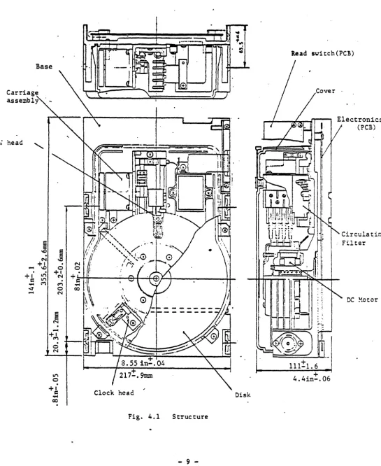
-4. STRUCTURE
4.1 External Size
See Fig. 4.1.
4.2 Unit Structure
The mini- disk drive unit consists of disks, heads, DC motor,
carriage assembly, cover, recirculation filter, base, read switch
(PCB), and logics (PCB).
(1) Disk
Disks are 100mm in inner diameter and 200mm in outer diameter
and are coated with a special lubricating material
(Winchester-type). Durability is over 10,000 starts and stops.
The numbc~ of disks per unit is two in the M230lA and four in the M2302A.
(2) Head
The Winchester-type heads are in contact with the disks when
the disks are not moving, but begin to fly when the
rotation reaches a certain speed.
The number of
the M2302A.
heads is four in the M230LA, and eight in
A similar head is used as the clock head, which.reads the
data written on the lower surface of the bottom disk to generate
~ndex, Sector, Write clock, Read clock and PLO clock signals.
(3) DC motor
The disks are rotated by a direct-drive DC motor. This motor
.
attains a very precise rotational speed of 2964 rpm±2% because
the current
is
controlled by comparing the phases of the clock-Base
Carriage asse:nbly
R/\\ head
~
-.0
.
N+1
-
.
-.0.
+1 Lt"I Lt"I
c: M
Of"! ..;:t
-i
-.0
.
0
+1 N
.
M0
N
§
N
·
LI"'I
o
·
+1 c:
.,..
co
·
Read switch(PCB)
Circ:ula tir:~
Filter
DC Hotor
Clock head Disk
Fig. 4.1 Structure
[image:13.626.25.570.68.733.2]-signal from the control circuit o~cillator and the clock signal read by the clock bead.
(4) Carriage assembly
This assembly consists of a 4-phase stepping motor. band actuator. viscose damper. and carriage with a linear bearing. The carriage working with the special 4rive circuit. gives increased reliability and a very short average access time of 7Oms.
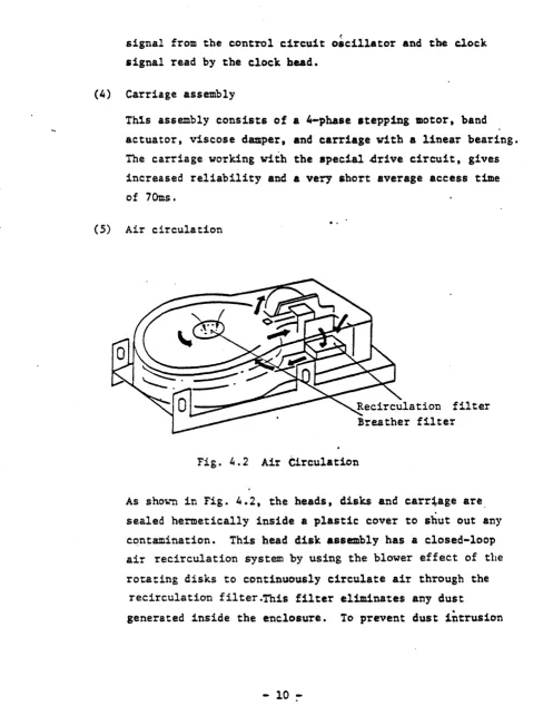
(5) Air circulation
Recirculation filter Breather filter
Fig. 4.2 Air Circulation
As sho~~ in Fig. 4.2. the heads. disks and earr~age are, sealed hermetically inside a plastic cover to shut out any contamination. This head disk assembly has a closed-loop air recirculation system by using the blower effect of the
rotating disks to continuously circulate air through the recirculation filter.This filter eliminates any dust
generated inside the enclosure. To prevent dust intrusion
[image:14.613.53.541.77.711.2]-due to pressure differences, a breather filter is attached at
the center of the disk where the pressure is lowest. This
breather filter equalizes the internal air pressure with
atmospheric pressure due to start up conditions and
temperature differences between the DE and its environment.
The filters used here are all absolute filters ~ith a dust elimination rate of 99.97% for particles O.3}lm or larger.
(6) Read/Write Circuit
The read/write circuits are designed using special analog
LSIs developed for large disk drive units. Use of these
LSIs simplifies circuitry and increases data reliability.
A VFO circuit and modulation/demodulation circuit for
MFM data are incorporated to reduce the controller's
cost and facilitate controller design.
(7) Stepping Motor Drive Circuit
The speed of the stepping motor is controlled by a speed
up/slow down control circuit that uses a ROM. It generates
an optimal pulse train and shortens access time. The
stepping motor is driven by two power supplies, so it
per-forms fast access with low power consumption when not seeking.
When 255 or more step pulses and the FALSE direction signal
(outer direction) are issued, the unit assumes the
Return-to-Zero (RTZ) instruction and automatically seeks to track O.
(8) DC Motor Drive Circuit
Rotational speed is controlled by comparing the byte clock
recorded in the clock track and a crystal oscillator signal.
This circuit thus maintains constant rotational spe~d.
-(9) Index/sector circuit
Index/sector signals are obtained from the index information in the clock track and the byte clock. The number of sec-tors can be set at the required value using switches on the printed-circuit board.
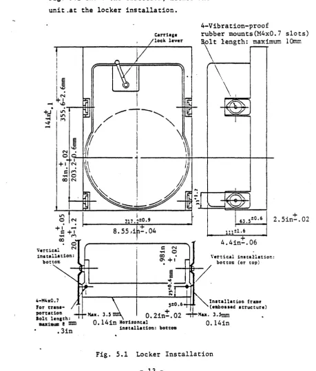
-5. INSTALLATION
5.1 Locker Installation
Fig. 5.1 shows the direction, method and frame structure of the
unit.at the locker installation.
...-4
.
+d ~ ~ ...-4
,
I ! II~
1\0
~~
\0
.
I~ ~..
c:C""'\~o «>N
Carriag_
lock lever
c: N
~ 0
«> •
Q'\
.
+ Ii
~---~---~
c---...
I ~
4-M4xO.7
4
For
trans-porut1ofl !1.ax. O. 2in!. 02
lolt iencth:
aax111UIC e mm O. 14 in Horizontal
.3in 1nstallat1oa: botto.
4-Vibration-proof
rubber mounts(M4xO.7 slots)
\t
length: maximum lOmm\\
\
I
63.S: 0 •6111 ~1.6
2.5in-:.02
Ver:ic~l 1nstallatior.:
bot to: (or tOJ))
In.tall_tioe frame
(.lIbo.led Itructure)
Hu. 3.Smm
0.14in
Fig. 5.1 Locker Installation
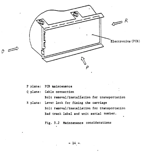
[image:17.615.74.534.179.719.2]5.2 Service Areas
The areas used for maintenance. securing the unit for trans-portation. and cable connection are the p. Q. and R planes sh~n in Fig. 5.2. Ease of maintenance should be considered
when deciding the system service clearance and locker instal-lation.
P plane:
Q plane:
R plane:
PCB maintenance Cable connection
~
p
Electronics (PCB)
Bolt removal/instal!ation for transportation Lever lock for fixing the carr-iage
Bolt removal/installation for transportation Bad track label and unit serial number.
Fig. 5.2 Maintenance considerations
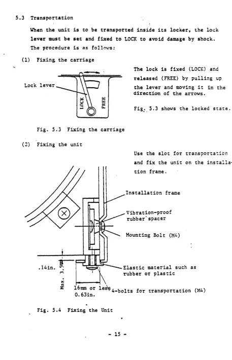
[image:18.620.68.534.257.763.2]5.3 Transportation
When the unit is to be transported inside its locker, the lock
lever must be set and fixed to LOCK to avoid damage by shock.
The procedure is as follcws:
(1) FixinS the carriage
Lock lever
The lock is fixed (LOCK) and
released (FREE) by pulling up
the lever and moving it in the direction of the arrows.
Fig:. 5.3 shows the locked state.
Fig. 5.3 Fixing the carriage
(2) Fixing the unit
.141n.
.
M
Fig. 5.4
Use the slot for trans?ortation
and fix the unit on the
installa-tion frame.
Installation frame
Vibration-proof rubber'spacer
Mounting Bolt (M4)
Elastic material such as rubber or plastic
l6mm or les\; 4-bolts for transportation (M4)
0.631n.
Fixing the Unit
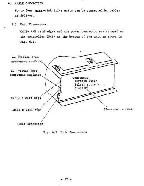
[image:19.627.69.527.75.786.2]-(3) Preventing connector disconnect
To prevent the connecting cables from disconnecting, they are retained by a cable holder as shown in Fig.
S.S.
The cable holder is fixed on the CNA and CNB surfaces by screws.
--~---~---~---I
I
I
I CNA
PO~~R eN
Fig. 5.5 Cable Holder
[image:20.624.56.525.75.734.2]-6. CABLE CONNECTION
Up to four mini-disk drive units can be connected by cables
as follows.
6.1 Unit·Connectors
'Cab1e A/B card edges and the power connector are arrayed on
the controller (PCB) at the bottom of the unit as show~ in Fig. 6.1.
A2 (viewed from component surfac
B2 (viewed from component surface
Cable A card
/
Cable B card edge /
/
/
Power connectorComponent surface (top) Solder su'rf ace (bottom)
Fig. 6.1 Unit Connectors
- 17 -.
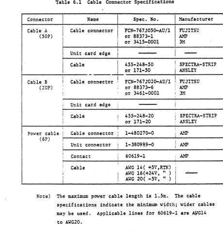
[image:21.613.78.559.119.741.2]6.2 Cable Connector Specifications
The recommended cable connector specifications are listed in
Table 6.1.
iable 6.1 Cable Connector Specifications
Connector
I
Name Spec. No. ManufacturerCable A I Cable FCN-767JOSo-AU/1 FeJITSU
I
connectorI
(SOP)
I
i
or 88373-1 or 341S-0001 AMP 3t-iI I
I
I
Unit card edge I I-I
I
I
Cable 4S5-248-S0 ! SPECTRA-STRIP
or 171-S0
I
ANSLEYI
-
-I I
I
Cable B I Cable connector I FCN-767J02D-AU/l ! FUJITSU
(20P) : : or 88373-6 j
A..~
I
! or 3461-0001 ! 3M
I Unit card edge ; f
I
! Cable ! 45S-248-20 I SPECTRA-STRIP
;
! I or 171-20
I
ANSLEY
,
; I
Po~'er cable I Cable connector I 1-480270-0
;
A.~i I
(6P) I :
i Unit connector I 1-38099.9-0 ! A.."!P
i ! I
i Contact 60619-1 AMP
i i
I
i I !
I
Cable AWG 14( +S'\',RTN) !
i I AWG l6(+24V, " ) I
-i !
AWG 20( -SV,
" ) I
I
! jNote) The maximum power cable length is l'.Sm. The cable
specifications indicate the minimum ~~dth; ~ider cables
may be used. Applicable lines for 60619-1 are AFG14
to AWG20.
[image:22.623.65.525.189.698.2]-6.3 Single Connection
Connection of one unit to its controller is shown in Fig. 6.2.
,
Cable A &B,1M
I
DRIVE ""t.J .I
CONTROLLER
Power cable
,
POWER SUPPLY ..I
Fig. 6.2 Single Connection
6.4 Connecting Multiple Units
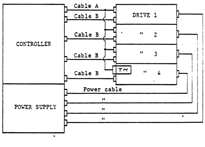
To connect ~o to four units, cable A (control signals) must be connected indaisy~chain and cable B (R/W signals) must be connected radially as shown in Figure 6.3 .
., Cable A r
CONTROLLER
.. DRIVE 1 nl--_ _
r ~
I
~~---~
~
Cable BI~
..
~~---~
~
., Cable B
..
"
2I
~
" 3h
., Cable B t ,.
~
1
~ I II
, Cable B
Y.
T MI
..
4tr-!
I '
~---~..
, Power cable~~---~
~
"
PO~~R SUPPLY ""
.,
"
"
Fig. 6.3 Connecting Multiple Units
[image:23.612.137.504.186.302.2] [image:23.612.149.490.443.687.2]-6.5 Driver/Receiver
See Fig. 6.4. The length specified is the maximum, and must not be exceeded when daisy-chained.
Control signal
R!\..' signal
I
i
l -i
+5V
Fig. 6.4 D=iver/ Receiver
6.6 DC Grounding
A tap (M4 x 0.7) is included for DC grounding at the location
indicated in Fig. 6.S. The scre~ must be M4 x 8 or smaller.
Cable holder DC grounding tap
Fig. 6.5 DC Grounding
[image:24.613.72.514.88.751.2]*(1 *(1
i • INTERFACE
This section describes the physical ahd logical conditions of the signals transferred through the interface between the disk drive and the.disk control unit. The timing is specified at the driver/
receivers of the unit.
7.1 Signal Lines
Controller sid e
(3) HEAD SELECT ~~2
(4) DRI'~ SELECT 1~4
(1) DIREC:IO~
(1) STEP
(1) FAU1.T CLEAR
(1) WRITE GATE
(1) READ GATE
paired) t-.'RI!'! DATA paired) t-.TP .. I TE CLock
12 lines + 2 pair s
Cable A
Drive side
INDEX (1)
READY (1)
SECTOR/BY!E CLOCK (1)
TRACK 0 (1)
WRITE FAu~T (1)
(SEEK COMPLETE) (1) *
READ DATA (1 paired)* PLO CLOCK (1 paired)*
6 lines + 2 p~irs
*
This signal line is connected bysetting a switch on the PCB. .
Cable B
CONTROLLER SIDE DRIVER SIDE
INDEX (1)
READY (1)
SECTOR/BYTE CLOCK (1)
SEEK COMPLETE (l)
(1 paired) ~~I!E DATA READ DATA (1 paired)
(1 paired) wiRI!E CLOCK PLO CLOCK (1 paired)
2 pairs 4. lines + 2 pairs
7.2 Input Signals
(1) Head Select 0 ~ 2
This signal line is used to select one of the eight or four
(in M230lA) data heads in the disk drive.
(2) Drive select 1 ~ 4
This signal line is used to select one of the four drive
units and validate the input/output signals of the selected
disk drive. The Drive Select 4 signal can be altered to the
Seek Complete signal by setting a swtich on the PCB.
(3) Direction
This siena1 line is used to oetermine the seek direction of
the data heads when the step pulses are given to the disk
drive. When this signal i~ true, seek is perforrnaned in an inward direction; when false. seek in performed in an outward
direction.
-(4) Step
This makes the data heads seek to one track in the
direc-tion indicated by the Direcdirec-tion signal at one of the
tran-sients (fales-t true) in the following modes:
(i) Controlled step mode
When the step pulse rate is 1 KHz or less, the drive responds to every step from the controller immediately.
(ii) Slave step mode
When the step pulse rate is between 3 KHz and 3MHz,
the drive does not begin seeking until after receiving all the step pulses and responds with the 5eek Complete signal after completing the seek operation.
(iii) Return to Zero Mode
When 255 or more step pulses are issued at slave mode, the date heads will move to Track 0 at a constant speed.
Note: Step rates between 1 KHz and 3 KHz are pro-hibited.
(5) Fault Clear
This signal line resets the write fault latch in the drive. The pulse width must be 100 ns or wider.
(6) Write Gate
This signal line gates WTite current to the selected data head in the drive.
(7) Read Gate
This signal is used to read from the selected data head in the drive. Read data is valid 8 bytes (13.5 JAs) after
Read Gate appears.
-23-(8) Write Data (balanced transmission)
This is a write data signal in the NRZ format and is
trans-mitted from the controller using balanced transmission lines.
It is synchronized with the leading edge of the Write Clock
signal in the drive.
(9) Write Clock (balanced transmission)
This is a write clock signal from the controller, and is
synchronized with the Write Data signal.
7.3 Output Signals
(1) Index
This is a pulse signal with a width of 1.7ps and is sent through CNA/B once per revolution of the disks in the
selected drive.
(2) Ready
This indicates that the rotational speed of the drive unit
has reached nominal speed, the PLO circuit is synchronized
with the rotational speed of the disk, and the drive is
selected. This signal is sent out ~hrough CNA/B.
(3) Sector (Byte Clock)
Sector or Byte Clock is selected by a switch on the PCB
in the drive unit. The signal is transmitted through CNA/B.
(i) Byte Clock
This is a pulse signal with a width of O.84~s, set for 12,000 bytes per track.
-(ii) Sector Mark
This is a pulse signal with a width of l.7ps. It is
generated by counting the number of bytes per sector
as selected on the PCB of the drive unit. Maximum is
4,096 bytes/sector.
(4) Track
°
.This indicates the data heads are stopped on track O.
(5) Write Fault
This indicates that one of the following abnormal states
occurred during writing, and is retained until reset by
Fault Clear.
(i)
(ii)
(iii)
(iv)
(v)
Write Gate was received before the drive unit was
ready.
Write Gate and Read Gate were received simultaneously.
Write Gate was received during multiple head select.
Write Gate was received when not SKC.
Appropriate write current did not flow through the
head during writing.
(6) Read Data (balanced transmission)
This is a read data signal in the NRZ format. This signal
is valid l3.5ps (8 bytes) after Read Gate, and is transmitted
synchronously with the leading edge of PLO Clock.
(7) PLO Clock (balanced transmission)
This is a l-bit interval pulse Signal. When reading is not
performed, PLO Clock is synchronized with the signal
-1
from the clock track. When reading is performed, the PtO is
syn-chronized with the Read Data signal from the data head.
PLO Clock is used as Write Clock by the controller during
_"r~ting.
(8) S~ek Complete
This indicates that the data heads are positioned
a: the requested track. This signal includes the settling time of the head, and when it is true, read/WTite operations are enabled. This signal is trahsmitted through CNA/B. Transmission through CNA is enabled by setting a switch on the PCB.
7.4 Timing Specifications
7.4.1 Seek timing
. (1) CO~TROLLED STEP MODE
STEP PULSES ---~
U
i •
I min 1.Oms
I
!
--..,jl
r--
100ns",,1.0~sI
( 2 ) SLA \~ STEP !-10DE
STEP PULSES
DIREcrIOl~
U
I
I
~'L
~
U
33Ons".330~s
---l
I--loons'\,250nsI
min lOOns
~
min lOOnsDRIVE SELECr _ _ 11111:=11 _ _ _ _ _ _ _ _ _ _ . . . ~
1--
min lOOns7.4.2 Read/Write Data Timing
(1) WRITE DATA, WRITE CLOCK
"1'''
"0" "1 "WRITE DATA
_ ... 1.
r-
210ns ---. II
t..'RITt CLOCK
Ons:30ns
(2) READ DATA, PLO CLOCK
RE..bJ) DATA
I
I
.r-
210ns-
II
PLO CLOCK
I
~I
E5ns~
I
I
~ ns20 ns 210ns
---1
-7.5 Formats
7.5.1 Track format
Example of a 40-sector format
"Index/Sector
Gap 1
17B Address Area 7B
Gap 2
l3B Sync. Data Area
Sync. Flag status
(1) Gap 1,2,3
Upper cyl.
(2) Sync." Pattern
7.5.2 Read/Write timing
(1) Write format
I!>"DEXI SECTOR
-1
\'''RITE GATEI
-i
I
t-3 Bits max
lB 2S6B
Lowler :Head Sec tor cy" \
all "0"
Address Area .. O!"
Data Area "09"
28
-CRe
Index/Sector
CRe
2B
eRe
Gap 3
(2) Write data
INDEX/stc~~ _ _ _ _ _ _ _ _ _ _ _ _ _ _ _ _ _ _
r L
I
Gap 1I
AA Gap 21
Data Gap31
READ GATE
I
J
I
I
--8 Bytes ~l Byte i
~'RITE GATE
2 Bytes
I
I
1 Byte(3) Read data
:~~!X/SEcrOR
~r-i
1____________________________________
n
~----I
j Gap 1 AA Gap 2 Data
I
I
--~
1 Byte~3 Bytes
~ 8
Bytes-I
,""---I' L l
I Bvte •R::AD GATE
7.6 Connector Positions
CNA
1
I.
Gl-i"D 2 - HEAD SELECT 03 : tI
4
..
15
"
6..
27
"
S SPARE9 '
"
10 -INDtX11
"
12-READY
13
"
14 -StCTOR/BYTE CLOCK15
"
16 -DRIVE SELECT 117
"
1S"
219
"
20 tt3
21
"
.22"
423 II
24 -DIRtCTION
:5
"
26 -STEP ,.27 " 28 -FAULT CLEAR
29
"
30 -t..'R!TE GATE31
"
32 -TRACK 0 33 I"
34 -t.."'RITE FAULT35 II
36 -READ GATE
37 " 38 G~"D
39 .;.t.,1UTE DATA 40 -wRITE DATA it1 I Gl\"D I 42 -WRITt CLOCK
43 +\'-'RITE CLOCK 144 G~"D
it5 +PLO CLOCK i
I
46 -PLO CLOCK 47 G~"DI
48 +READ DATAI
~9 -READ DATA
I
50 GNDKey slot: Between 4P and 5P
cm
I
I
1 -INDEX
I
2 GND3 I I -READY i 4
"
I
5
.j
- SECTOR/BY!E CLOCK ! 6 It!
!7 I -SEEK COMPLETE 8 I "
9 +WRITE DATA ! 10
I
-WRITE DATAt I
11 G~'D ! 12
I
+WRITE CLOCK13 -WRITE CLOCK 114 ; Gh"D
I !
15 +PLO CLOCK ; 16 ! -:PLO CLOCK
17 G!\'D
118 '
+R.tAD DATA19 -READ DATA . 1 20 G~""D
Key slot: Between 4P and SP
7.7 Power Supply Input Connector
1 +24V 2 +24V RTN
3 - 5V RTN 4 - 5V
5 + 5V 6 + 5V Ron;
-8. PO~~R SUPPLY CONDITIONS
8.1 Input Voltage and Permissible Input Voltage Variation
Input voltage
+24V +24V:10%
+ 5V + 5\1:5%
- 5V
The above values are voltages at the.power supply input
terminal section of the unit.
8.2 Current Values
Peak Average current
current Not seeking Seeking
+24\1 6.0A 1.2A l.6A
+SV 6.0A 4.0A 4.1A
-5V O.SA O.5A O.5A
The average current during seeking ii the value at the
time of: (average seek) + (latency time) + (reading or
~~i:ing during one revolution).
8.3 Power Consumption
Not seeking
Seeking
Sl.3W
6l.4W
-8.4 Current Waveforms
(1) +24V current waveform
6A~I ______________ ~ ______ _
I
4 .5A ~ _ _ _ _ _ ...
I
3AI ~ ____________ ~--__ ~
DC motor activation
Ready
(Not seeking) Seeking
I
Expansion of B section
3 A - - - _
OA---f
- 33 - .
Expansion of C section
0 3
A A.
Jl
loo...---..j/l,-
Same waveform as that of B section (average current 1.2A)3A
OA---f
lms+ 0 ~ 2ms
+
The ~aveform of the C section is obtained by superimposing the above two waveforms as)~chronously.
(2) +5\' current waveform
+5\' current has a sat.;tooth waveforJD during seeking, as shot.,"n
beloio.~ .
6.0A
2. SA _ _ _ _ _ ~J_
S KC =====::11
1\
\II
\1
- 34
-Even-numbered cylinder 4.lA Odd-numbered cylinder 3.3A
Expansion of A section
6 . 0 A - - -....
3.3A
----!~
l.()'\Jl.Sms l.S'V2.0ms
Note) The peak current (6A) in the A section flows only 3 or 4 times during one seek.
8.5 Power ON/OFF Sequence
~~en the Write Gate signal from the controller is off before
the power is on or off, the power (+24V, +SV, -SV) need not be sequenced. That is, recorded data will not be destroyed and mechanical or electric troubles will not occur. To
maintain the Write Gate ~ignal in the off state at the time of unit power-on or -off, the power supply of the controller and drive unit must be sequenced as follows:
(1) Basic sequ.ence
I
Controller 90~
power supply ____ __ (all power'
supplies)
I
I
I tDisk drive unit I 10%
power supply
---1--1
(+24V ,+5V ,-5\1)
--, Tl
r--Tl, T2: 0 sec. or longer 10%
1
---;T2-I ., 90%
Note) The power supplies of the disk drive unit (+24V, +5\' t
-5V) need. not ~e sequ~nced.
(2) When the +5V for the disk drive is supplied from the controller power supply and the interface signal from the
controller is determined by the +5V controller power supply, the voltage level of +5V is detected in the
drive unit and Write Gate signal is inhibited. Sequencing
is therefore unnecessary.
8.6 Others
(1) To eliminate AC line noise, a noise filter of the
specifi-cations given below should be incorporated in the AC input
terminal of the disk drive power supply.
Attenuation characteristic
Circuit configuration
- 36
-40dB or greater at lOMHz
T type shown below is recommended.
9. MAINTENANCE PARTS
The maintenance parts replaceable in the field are shown in
Table 9.1.
Table 9.1 Maintenance Parts
I
I
I.tem
!
Part name Part No.I
Qty/unit1
I
Controller (PC!)I
I
B16B-6840-8020AI
12
I
Head pre-amplifier (PCB)I
B16B-6990-0020A.
i
I 1I
!
37
-I
\
I
[image:41.624.95.518.114.299.2]Notes for connecting the M2301/M2302 to a controller.
1. Power Supply
(a) The H2301n!2302 needs DC +5V, +24V and -5V. The current of
each voltage is as follows:
(1) +SV DC Average 4.1A
Peak 6.0A (Pulse current)
(2) +24V DC Average l.7A
Peak '4.5A (Start-up cycle, 10 seconds) Note: For +24V, we recommend using a 4.SA power supply.
(3) -SV,DC O.SA (Stable)
Note: -12V cannot currently be substituted for -5V. See Section 5.
Before connecting tr~ power supply to the drive, please make sure tha t the above requiremeo,ts are s~ tisfied. FAI can, if necessary, provide a power supply for your evaluation of the drive.
2. S~itch Options
(a) The l-12301 /~12302 has several s\o.Titch options for SA4000 interface compatibility.
Before you exercise the drive, please verify all switch settings, using the operation manual. The PLO signal on the interface is already inverted.
3. Data Format
Read Gate
Write Gate
(a) At Gap 2 on the data format, the signal Read Gate should be lo~
for more than 1 byte. Sector
Gap 1 Gap 2 Gap 3
ID I I Data I
I I I I
~
,
....4 byte min ...
>1 byte
--...
r-
...---J
,
-->
,
byte~1
""- > 1 byte"
38
(b) The timing si~nals, Write Gate and Read Gate, should satisfy t>l byte, as in the diagram, in order to avoid a write splice.
4. Cabling
(a) If two cables (50 pin and 20 pin) are used with the controller, Read Data Clock and Write Data should not appear on the "Au
cable. This is accomplished through the switch settings on Switch 4.
(b) The PCB connectors for the cables are labeled on the component side as even numbers, 02 - 20 and 02 - 50. When the drive is in the horizontal place, Pin I is on the right
1(facing the connectors) upper side of the PCB.
5. Jumper -aption~
(a) PLO Cleek +
location: D,C,3,4
position for normal clock
Ba
eN Bc:=DTP
position for inverted PLO Clock
Cj~ B
c:::J DTP
(b) DIRECTI,)~1/ STP :iming (Logic levels) loca tion ~ Cl;
Position when triggering on trailing edge of STP (SA4000)
r~ Jumper
I • ''1 DIRECTION
~
______________
~:,~c______________ __
lrall'"~
'WI"
:rI:-~) ~
(
~.
.. 16
----, I .---;
-;r---lrr
STP
~4
200::
:in
SEEK COMPLETE
u
l.
*
.r
*
SEEK COMPLETE must occur 1ms after last STP-- position when triggering on leading edge of STP
L
Jumperr ., I
fall "
I~IIO DIRECTION ~J---~Lr'---~
'e'"
?
L_~(
i
100-ns ...
J
[l---).r'~
ml.nSTP
(c) Voltare selection
Location: E3
•
Currently the drive will operate only with pins 1-2 jumpered for -5V.
later versions of M2301/2 will allow jumperi~g pins 2-3 in order to accept -12V.
40
APPENDIX 1. l1EDIA ERROR
(1) Media Error Display Method
A defective area of the M2301/M2302 media is located with reference
to the Physical Index by the number of bytes from the Physical
Index. The Physical Index represents the Index Pattern Division
recorded on the clock track. The relationships of the Physical
Index and Interface Index/Sector are as shown below.
Physical Index
___
n~
____________ _
Interface Index
_I~n~_
'"~
•
•Interface Section ----~--~
~---~A A~
A: This represents the number of bytes of one sector.
(2) Relation of the Defective Area Display Value and the Defective Sector.
The defective sector number can be calculated from the defective
area display value by uSing the following formula.
Defective Sector Number =
[X) -
1Note 1: X: Defective position display value A: Number of bytes of one sector
(]:
This indicates that all the numbers after the decimal point are to be omitted.For example:
~.~
=
21: Compensates for the difference between Physical and Interface Index.
-1-Note 2: The sector next to the index is assumed to be the
o
sector.Index
____
~n~________________ _
Sector
N
o
1I
2The following 2 examples indicate how the defective sector
number can be calculated.
[ExamPle 2J
x
=
800A =: 300
Defective sector number = [800] _ 1 300
x =
200A = 300
-= 2 - 1.
= 1
1 sector is defective
Defective sector number = [200] _ 300 1
= 0 - 1
= -1
N (last) sector is defective
-2-APPENDIX 2. SWITCH SETTING PROCEDURES
The functions and assignment procedures of the different switches on
the PCB of the M2301/M2302 system are described below.
(1) DRIVE SELECT (Device Number Selector)
The drive select switch is used to select one of the maximum 4
devices to be connected. Of·the 4 keys, you are to turn ON only the relevant key, while turning OFF the other 3. The device
number selection configurations are shown in Table 1 and Figure 1.
Table 1 Device Number Selection
Device Number SW3 Switch
1
2
3
4
Key 8 Key 7 Key 6 Key 5
0 x x x
x 0 x x
x x 0 x
x x x 0
SW3 (Mounting position B6)
The figure at left shows
OFF ON the configuration for
0: ON
x: OFF
•
'15 lCey 5 selecting Device Number 1.•
16 Key 6•
j 7 Key 7-8 Key 8
Figure 1. Device Selecting Switch
[image:47.626.89.562.107.771.2]-3-(2) SEEK COMPLETE
When sending the SEEK COMPLETE signal (name: SEEK COMPLETE) onto
. :.t'lIlie A cable of the interface, turn on Key 4 of SW3. However, at
this point, be sure not to leave DRIVE SELECT 4 in the'ON status (see Figure 2).
SW3 (Mounting position B6)
OFF ON
::::'::"::::3
-4
C~':::=5
Key 3 Key 4 Key 5
The procedures shown in the figure at left are to be used when
sending the SEEK" CO~~LETE signal.
Figure 2. SEEK COMPLETE SWITCH
(3), _~ ~;SECTOR 'BYTE t:LOCK
.~ ·\This switch is used to send either the SECTOR or BYTE CLOCK signal into the interface cable. The switch configurations are shown in
Table 2 and Figure 3 below.
Table 2 SECTOR/BYTE CLOCK
Signal SW2 Switch
Name
Key
.,
Key 2
.-SECTOR 0 x
BYTE CLOCR x 0
SW2 (Mounting position T4)
OFF
ON•
""-~12 I.ey 2 Key 3Figure 3 SECTOR/BYTE CLOCK
-4-0: ON
x: OFF
[image:48.615.64.532.64.763.2](4) SECTOR During the Generation of INDEX
This is used to select whether or not to send the sector mark,
generated in the same timing with the index onto the interfat~.
The switch configurations are shown in Table 3 and Figure 4;~',
Table 3 SECTOR During the Generation of INDEX
SW?
Selection content
f--Key 1
<lend the SECTOR x
--Do not send the SECTOR 0
SW2 (Mounting position T4)
OFF - ON
___ ... _1 Key 1
____ ... 11 by 1
-
o:ONx:OFF
The figure at left shows the switch conf.i.guration when the INDEX/SECTOR is not sent simultaneously.
Figure 4. SECTOR During the Generation of INDEX
(5) WRITE/READ DATA and WRITE/PLO CLOCK
The method of sending the WRITE/READ DATA and WRITE/PLO CLOCK signals onto the A cable of the interface is shown in Table 4 and Figure 5.
Table 4 W /R DATA and l\T
IP
CLOCKSignal Name Assigned Switch SW4
+WRITE DATA Key 7, Key 8 ON
+READ DATA Key 1, Key 2'ON
+WRITE CLOCK Key 5, Key 6 ON
+PLO CLOCK Key 3, Key 4 ON
[image:49.626.73.553.177.754.2]-5-SW4 (Mounting position
OFF ON
~'_l E.ey 1
• 2.
..
2. 3
..
3.4
..
4.5
..
5.6
..
6• 7
..
7.8
..
8B5)
The figure at left shows the switch configuration
when all the signals are to be sent •
Figure 5. W/R DATA and W/P CLOCK
(6) Sector Count Selection
The number of sectors can be selected by using the keys of switches
··SWI and SW2. The key of the respective switches corresponds to
~20 through 211 bytes. (See Table 5)
~
Table 5 Sector Counter Byte Table
SWI No of Bytes SW2 No of Bytes
Key 8 1 Key 8 256
Key 7 2 Key 7 512
Key 6 4 Key 6 1024
Key 5 8 Key 5 2048
Key 4 16
Key 3 32
Key 2 64
Key 1 128
Various configurations of the switches are shown in Tabl~ 6 and Figure 6t where the LAST SECTOR indicates the number of excess
bytes. This also indicates' that only the number of excess bytes
becomes longer.
[image:50.620.102.533.53.762.2]-6-Table 6 Sector Configurations
SECTORS SW1 SW2 BYTES/SECTOR LAST SECTOR
8 7 6 5 4 3 2 1 8 7 6 5
2 1 1 1 1 1 1 1 1 1 1 1 1 4095 +3810+32 -0 3 0 0 0 0 0 1 0 1 1 1 1 1 4000 0
"
4 0 0 0 1 1 1 0 1 1 1 0 1 3000 0"
5 0 0 0 0 0 1 1 0 1 0 0 1 2400 0"
6 0 0 0 0 1 0 1 1 1 1 1 0 2000 0
"
7 0 1 0 0 1 1 0 1 0 1 1 0 1714 +2"
8 0 0 1 1 1 0 1 1 1 0 1 0 1500 0..
9 1 0 1 0 1 1 0 0 1 0 1 0 1333 +3 tt10 0 0 0 0 1 1 0 1 0 0 1 0 1200 0
"
11 0 1 0 0 0 0 1 0 0 0 1 0 1090 +10"
12 0 0 0 1 0 1 1 1 1 1 0 0 1000 0"
13 1 1 0 1 1 0 0 1 1 1 0 0 923 +1"
14 1 0 0 1 1 0 1 0 1 1 0 0 857 +2"
15 0 0 0 0 0 1 0 0 1 1 0 0 800 0"
16 0 1 1 1 0 1 1 1 0 1 0 0 750 0"
17 1 0 0 0 0 0 1 1 0 1 0 0 705 . ,+15"
18 0 1 0 1 1 0 0 1 0 1 0 0 666 .+12"
19 I' 1 1 0 1 1 "I 0 0 1 0 0 631 '+11 It20 0 0 0 1 1 0 1 0 0 1 0 0 600 0
"
2·1I
1 1 0 1 1 1 0 0 0 1 0o :
571 +9 It22 1 0 0 0 0 1 0
a
0 1 0 0 545 +10"
23 1 0 0 1 0 0 0 0 0 1 0 0 521 +17"
24 0 0 1 0 1 1 1 1 1 0 0 0 500 .. " "~'; 0"
25 0 0 0 0 0 1 1 1 1 0 0 0 480 \ 0
"
26 1 0 1 1 0 0 1 1 1 0 0 0 461 +14"
27 0 0 1 1 1 1 0 1 1 0 0 0 444 +12"
28 0 0 1 1 0 1 0 1 1 0 0 0 428 +16"
29 1 0 1 1 1 0 0 1 1 0 0 0 413 +23"
30 0 0 0 0 1 0 0 1 1 0 0 0 400 0"
31 1 1 0 0 0 0 0 1 1 0 0 0 387 +3"
32 0 0 0 1 1 1 1 0 1 0 0 0 375 0"
33 1 1 0 1 0 1 1 0 1 0 0 0 363 +21"
34 0 0 0 0 0 1 1 0 1 0 0 0 352 +32"
35 0 1 1 0 1 0 1 0 1 0 0 0 342 +30"
36 . l' 1 0 1 0 0 1 0 1 0 0 0 333 +12"
37 0 0 1 0 0 0 1 0 1 0 0 0 324 +12"
38 1 1 0 1 1 1 0 0 1 0 0 0 315 +30"
39 1 1 0 0 1 1 0 0 1 0 0 0 307 +27"
40 0 0 1 1 0 1 0 0 1 0 0 0 300.
0"
50 0 0 0 0 1 1 1 1 0 0 0 0 240 0"
60 0 0 0 1 0 0 1 1 0 0 0 0 200 0"
70 1 1 0 1 0 1 0 1 0 0 0 0 171.
+30"
80 0 1 1 0 1 0 0 1 0 0 0 0 150 0"
[image:51.618.74.558.118.729.2]Table 6 Sector Configuration (cont'd)
SECTORS SWI SW2 BYTES/SECTOR LAST SECTOR
8 7 6 5 4 3 2 1 8 7 6 5
90 1 0 1 0 0 0 0 1 0 0 0 0 133 +30+32
-0
100 0 0 0 1 1 1 1 0 0 0 0 0 120 0
"
110 1 0 1 1 0 1 1 0 0 0 0 0 109 +10"
120 0 0 1 0 0 1 1 0 0 0 0 0 100 0"
130 0 0 1 1 1 0 1 0 0 0 0 0 92 +40"
"0" indicates the OFF and "1" indicates the ON status.
SW1 (Mounting position T5)
SW2 (Mounting position T4) OFF ON
Key 1
•
1112
..
2-
The figure at left. 3
"
3 indicates the switch-
14"
4 OFF ON selectionconfigura-5
• 5 It 5
•
15 Key tion for 40 sectors •• 6
"
6•
16..
6•
17 It 7•
17..
7-
18"
8 - 8 If8
Figure 6. Sector Configuration
[image:52.617.42.565.66.768.2] [image:52.617.28.580.183.768.2]-8-(7) DELAY SKC
This is used to select whether or not to send SEEK COMPLETE (signal name: SEKC) with SETTLING TIME or SEEK COMPLETE (signal name: SKC) without SETTLING TIME to SEEK COMPl,.E;'!l!;;on the interface. The switch configurations are shown in } Table 7 and Figure 7.
Table 7 DELAY SKC
Signal Name SW3
Key 1
SEKC 0
,",
SKC x
SW3 (Mounting position B6)
•
OFF ON'---____ -.1
Key 1Figure 7. DELAY SKC (8) Controlling the Basic DRIVE SELECT Signals
0: ON
x: OFF
The figure at left sho¥1s the switch configuration for sending the SEKC.
Even when the relevant devices are not selected, the four basic Signals (INDEX, DRIVE READY, SECTOR/BYTE CLOCK and SEEK COMPLETE) can be sent to the interface cable (both A and B). The configura-tions for sending these Signals are shown in Table 8 and Figure 8.
[image:53.641.80.557.96.755.2]-9-Table 8 Controlling the DRIVE SELECT Signals
A cable
...
! ~ates
t
:lJ~~s not
, - '
SW3 SW3
B cable
Key 2 Key 3
~
, . ,
--1
0 Gates 0
,0 ,~ • • 0: ON
",
gate' x Does' not 'gate x , ~: OFF
1,
SW3 (Mounting~position B6)
1.O~ ON
,., - 2
• 1.3
Key 2
lCey 3
·!be figure at left shows th~< ",_witch configuration when-·'ip.e"
A cable is gated leaving th~~ B cable ungated.
Figure 8 Controlling the DRIVE SELECT Signals
(9) Time Hargin l'leasuring Switch
This switch is usually used in the "ON" status. However, when
!.tn...~~~ring the margin, this is turned HOFF".
SW2 (Mounting position T4)
OFF ON
__ -_4'
:~ey 4 The configuration at leftindicate~:' tb~i1ormal operating positioD(d!---the switch.
Figure 9 Time Margin Measuring:-Swi~ch
[image:54.617.99.524.75.735.2]