950 Rittenhouse Rd. Norristown, PA 19403 (215) 666-7950
(=:
NMOS CMOS
LCD
Component Data Catalog 1981
Section 1
Numerical and Functional Indexes
Replacement Part Cross Listings
Section
2
NMOS
Section
3
CMOS
Section
4
LCD
Section 5
Packaging and
I
I
I
I
I
I
I
I
I
I
I
I
I
I
I
I
I
I
I
I
I
I
I
I
I
I
I
I
I
I
I
I
I
I
I
I
I
I
I I I I I I I I
I
I I I I I I I
I
I I I
I
I I I I
I
I I I I I I I
I
I I I
I
I I
I I I I I I
I
I I I I
I
I I I
I
I I I I I I
I
I I I I
I
I I I
I
I I I I I I
I
I I I
NUMERICAL INDEX
2114 Static RAM (1024 X 4) ... 2-102 2316 Static ROM (2048 X 8) ... 2-106 2332 Static ROM (4096 X 8) ... 2-109 2364 Static ROM (8192 X 8) ... 2-112 6500 ... 2-1
6500/1 One-Chip, 8-Bit Microcomputer ... 2-15
6502 Microprocessor ... 2-11 6503 Microprocessor ... 2-11 6504 Microprocessor ... 2-11 6505 Microprocessor ... 2-12 6506 Microprocessor ... 2-12 6507 Microprocessor ... 2-12 6508 Microprocessor ... 2-18 6512 Microprocessor ... 2-13 6513 Microprocessor ... 2-13 6514 Microprocessor ... 2-14 6515 Microprocessor ... 2-14 6520 Peripheral Adapter ... 2-27 6522 Versatile Interface Adapter (VIA) ... 2-35 6523 Tri-Port Interface ... 2-48 6525 Tri-Port Interface ... 2-53 6530 Memory-I/O-Timer Array ... 2-61 6532 Memory-I/O-Timer Array ... 2-67 6560 Video Interface Chip (VIC) ... 2-73 6561 Video Interface Chip (VIC) ... 2-73 6562 Video Interface Chip (VIC) ... 2-86 6563 Video Interface Chip (VIC) ... 2-86 65245 Octal Bus Transceiver with 3-State Outputs ... 2-100
FUNCTIONAL INDEX Microprocessors
6500 ... 2-1
6500/1 One-Chip, 8-Bit Microcomputer ... 2-15
6502 Microprocessor ... 2-11 6503 Microprocessor ... 2-11 6504 Microprocessor ... 2-11 6505 Microprocessor ... 2-12 6506 Microprocessor ... 2-12 6507 Microprocessor ... 2-12 6508 Microprocessor ... 2-18 6512 Microprocessor ... 2-13 6513 Microprocessor ... 2-13 6514 Microprocessor ... 2-14 6515 Microprocessor ... 2-14
Peripheral Devices
RaiKIom
Access Memories2114 Static RAM (1024 X 4) ... 2-102
Read-Only Memories
2316 Static ROM (2048 X 8) ..•... 2-106
2332 Static ROM (4096 X 8) ... 2-109
2364 Static ROM (8192 X 8) ... 2-112
STATIC RAM PART NUMBER REPLACE WITH
PART NUMBER
REPLACE WITHPART NUMBER
REPLACE WITH IntersiJ MOS Technology Intel MOS TechnologyAMD MOS Technology
AM9114BPC
MPS2114-45
AM9114BDC
MCS2114-45
AM91L 14BPC
MPS2114L-45
AM91L 14BDC
MCS2114L-45
AM9114CPC
MPS2114-30
AM9114CDC
MCS2114-30
AM91L 14CPC
MPS2114L-30
AM91L 14CDC
MCS2114L-30
AM9114EPC
MPS2114-20
P2114
MPS2114-45
P2114L
MPS2114L-45
P21143
MPS2114-30
P2114L3
MPS2114L-30
P21142
MPS2114-20
P2114L2
MPS2114L-20
Motorola MOS Technology
MCM2114P-45 MPS2114-45
MCM2114C-45 MCS2114-45
MCM21L 14P-45 MPS2114L-45
P2332
MPS2332
C2332
MCS2332
Motorola MOS Technology
MCM68316B
MPS2316
MCM68332
MPS2332
National MOS Technology
MM2316B
MPS2316
MM52132
MPS2332
MM52164
MPS2364
AM9114EDC
MCS2114-20
MCM21L 14C-45 MCS2114-45
NEC MOS TechnologyAMI MOS Technology
52114-3
MP52114-30
52114L-3
MP52114L-30
52114-2
MP52114-20
52114L-2
MP52114L-20
EMM
MOS·
TechnologyMCM2114P-30 MPS2114-30
MCM2114C-30 MCS2114-30
MCM21L 14P-30 MPS2114L-30
MCM21L 14C-30 MCS2114L-30
MCM2114P-20 MPS2114-20
MCM2114C-20 MCS2114-20
MCM21L 14P-20 MPS2114L-20
UPD2316B
MPS2316
UPD2332
MPS2332
UPD2364
MPS2364
Signetics MOS Technology
2632N
MPS2332
2664N
MPS2364
2114UCB
MPS2114-45
MCM21L 14C-20 MCS2114L-20
T.I. MOS Technology2114UCA
MCS2114-45
L2114UCB
MP52114L-45
L2114UCA
MC52114L-45
2114-3CB
MPS2114-30
2114-3CA
MCS2114-30
L2114-3CB
MP52114L-30
L2114-3CA
MCS2114L-30
2114-2CB
MPS2114-20
2114-2CA
MCS2114-20
L2114-2CB
MPS2114L-20
L2114-2CA
MCS2114L-20
T.I. MOS Technology
TMS4045-45NL MPS2114-45
TMS4045-45jL
MCS2114-45
TMS40L45-45NL MPS2114L-45
TMS40L45-45jL MCS2114L-45
TMS4045-30NL MPS2114-30
TMS4045-30jL
MCS2114-30
TMS40L45-30NL MPS2114L-30
TMS40L45-30jL MCS2114L-30
TMS4045-20NL MPS2114-20
TMS4045-20jL
MC52114-20
TMS4732NL
MPS2332
TMS4732jL
MCS2332
TMS4764NL
MPS2364
TMS4764jL
MCS2364
Mostek MOS Technology
MK31000N-3
MCS2316
MK31000P-3
MPS2316
MK36000P-5
MPS2364
MK36000N-5
MCS2364
MICROPROCESSORS Fujitsu MOS Technology
MB8114N
MPS2114-30
ROMSynertek MOS Technology
SYP
=
Plastic
MPS
=
Plastic
MB8114NL
MPS2114L-30
AMD MOS TechnologySYC
=
Ceramic MCS
=
Ceramic
MB8114E
MPS2114-20
AM9217BPC
MPS2316
SYP/C6502
MPS/CS6502
MB8114EL
MPS2114L-20
AM9217BDC
MCS2316
SYP/C6503
MPS/CS6503
Hitachi MOS Technology
HM472114-4
MCS2114L-45
AM9232BPC
MPS2332
AM9232BDC
MCS2332
SYP/C6504
SYC/C6505
MPS/CS6504
MPS/C56505
Intel MOS Technology
P2114
MPS2114-45
C2114
MCS2114-45
AMI MOS Technology
568316A
MPS2316
568332
MPS2332
SYP/C6506
MPS/CS6506
SYP/C6507
MPS/CS6507
SYP/C6512
MPS/CS6512
SYP/C6513
MP5/CS6513
P2114L
MPS2114L-45
EA MOS TechnologySYP/C6514
MPS/CS6514
C2114L
MCS2114L-45
EA2316B
MPS2316
SYP/C6515
MPS/CS6515
P2114-3
MPS2114-30
C2114-3
MCS2114-30
P2114L-3
MPS2114L-30
C2114L-3
MCS2114L-30
P2114-2
MPS2114-20
EA2332
MPS2332
G.I. MOS Technology
RO-3-9316B
MPS2316
RO-3-9332B
MPS2332
A
=
2MHz
A
=
2MHz
B
=
3MHz
B
=
3MHz
5YP/C6502A
MPS/CS6502A
SYP/C6502B
MPS/CS6502B
C2114-2
MCS2114-20
Intel MOS TechnologySYP/C6503A
MPS/CS6503A
P2114L-2
MPS2114L-20
P2316B
MPS2316
SYP/C6503B
MPS/CS6503B
MICROPROCESSORS (CONT.)
PART NUMBER
REPLACE WITHPART NUMBER
REPLACE WITHPART NUMBER
REPLACE WITH Rockwell MOS Technology Rockwell MOS Technology Synertek MOS TechnologySYP/C6504B
MPS/CS6504B
SYP/C6505A
MPS/CS6505A
SYP/C6505B
MPS/CS6505B
SYP/C6506A
MPS/CS6506A
SYP/C6506B
MPS/CS6506B
SYP/C6507A
MPS/CS6507 A
SYP/C6507B
MPS/CS6507B
SYP/C6512A
MPS/CS6512A
SYP/C6512B
MPS/CS6512B
SYP/C6513A
MPS/CS6513A
SYP/C6513B
MPS/CS6513B
SYP/C6514A
MPS/CS6514A
SYP/C6514B
MPS/CS6514B
SYP/C6515A
MPS/CS6515A
SYP/C6515B
MPS/CS6515B
SYP6520
MPS6520
SYP6520A
MPS6520A
SYC6520
MCS6520
SYC6520A
MCS6520A
SYP6522
MPS6522
SYP6522A
MPS6522A
R6502P
MPS6502
R6502AP
MPS6502A
R6502C
MCS6502
R6502AC
MCS6502A
R6503P
MPS6503
R6503AP
MPS6503A
R6503AC
MCS6503A
R6504P
MPS6504
R6504AP
MPS6504A
R6504C
MCS6504
R6504AC
MCS6504A
R6505P
MPS6505
R6505AP
MPS6505A
R6505C
MCS6505
R6505AC
MCS6505A
R6506P
MPS6506
R6506AP
MPS6506A
R6506C
MCS6506
R6506AC
MCS6506A
R6507P
MPS6507
R6507AP
MPS6507A
R6507C
MCS6507
R6507AC
MCS6507A
R6514P
MPS6514
R6514AP
MPS6514A
R6514C
MCS6514
R6514AC
MCS6514A
R6515P
MPS6515
R6515AP
MPS6515A
R6515C
MCS6515
R6515AC
MCS6515A
R6520P
MPS6520
R6520AP
MPS6520A
R6520C
MCS6520
R6520AC
MCS6520A
R6522P
MPS6522
R6522AP
MPS6522A
R6522C
MCS6522
R6522AC
MCS6522A
R6530P
MPS6530
R6530C
MCS6530
R6532P
MPS6532
R6532AP
MPS6532A
R6532C
MCS6532
R6532AC
MCS6532A
SYC6522
MCS6522
R6512P
MPS6512
R6500/IP
MPS6500/1
SYC6522A
MCS6522A
R6512AP
MPS6512A
R6500/IAP
MPS6500/IA
SYP6530
MPS6530
R6512C
MCS6512
R6500/IC
MCS6500/1
SYC6530
MCS6530
R6512AC
MCS6512A
R6500/IAC
MCS6500/IA
SYP6532
MPS6532
R6513P
MPS6513
SYP6532A
MPS6532A
R6513AP
MPS6513A
SYC6532
MCS6532
R6513C
MCS6513
Section 2
NMOS
6500 Microprocessors
• Single +5V Supply • 13 Addressing Modes
• N-Channel, Silicon-Cate, Depletion-Load Technology • Programmable Stack Pointer and Variable-Length Stack • 8-Bit Parallel Processing • Usable With Any Type or Speed Memory
• 56 Instructions • 1 or 2 MHz Operation
• Decimal and Binary Arithmetic • Pipelined Architecture DESCRIPTION
The 6500 Series microprocessors represent the first totally software-compatible microprocessor family. This family of products includes a range of software-compatible microprocessors which provide a selection of addressable memory range, interrupt input options and on-chip clock oscillators and drivers. All of the microprocessors in the 6500 group are software-compatible within the group and are bus compatible with the M6800 product offering.
The family includes five microprocessors with on-board clock oscillators and drivers and four microprocessors driven by external clocks. The on-chip clock versions are aimed at high-performance, low-cost applications where single-phase inputs, c~ystal or RC inputs provide the time base. The external clock versions are geared for multi-processor system applications where maximum timing control is mandatory. All versions of the microprocessors are available in 1 MHz and 2 MHz
CA"
suffix on product numbers) maximum operating frequencies.MEMBERS OF THE FAMILY Part Numbers
Plastic Ceramic Clocks Pins MPS6502 MPS6503 MPS6504 MPS6505 MPS6506 MPS6507 MPS6512 MPS6513 MPS6514 MPS6515 PIN FUNCTIONS Clocks (<1>1 and <1>2)
MCS6502 MCS6503 MCS6504 MCS6505 MCS6506 MCS6507 MCS6512 MCS6513 MCS6514 MCS6515
On-Chip 40
"
28"
28"
28"
28"
28External 40
"
28"
28"
28The 651X requires a two-phase, non-overlapping clock that runs at the Vee voltage level.
The 650X clocks are supplied with an internal clock gener-ator. The frequency of these clocks is externally con-trolled. Details of this feature are discussed in the 6502 portion of this data sheet.
Address Bus (AO-A 15)
(See sections on each processor for respective address lines on those devices.)
These outputs are TTL-compatible, capable of driving one standard TTL load and 130pF.
2-1
IRQ NMI ROY Addressing
V
V
V
16 (64 K)V
V
12 (4 K)V
13 (8 K)V
V
12 (4 K)V
12 (4 K)V
13 (8 K)V
V
V
16 (64 K)V
V
12 (4 K)V
13 (8 K)V
V
12 (4 K)Data Bus
(00-07)
Eight pins are used for the data bus. This is a bi-directional bus, transferring data to and from the device and peripherals. The outputs are three-state buffers capable of driving one standard TTL load and 130pF.
Data Bus Enable (DBE)
Ready (RDY)
This input signal allows the user to single-cycle the microprocessor on all cycles except write cycles. A nega-tive transition to the low state during or coincident with phase one ({{I1) will halt the microprocessor with the out-put address lines reflecting the current address being fetChed. This condition will remain through a subsequent phase two ({{I2) in which the Ready signal is low. This feature allows microprocessor interfacing with low-speed PROMS as well as fast (max. 2 cycle) Direct Memory Ac-cess (DMA). If Ready is low during a write cycle, it is ignored until the following read operation.
Interrupt Request (IRQ)
This TIL -compatible signal requests that an interrupt se-quence begin within the microprocessor. The microprocessor will complete the current instruction being executed before recognizing the request. At that time, the interrupt mask bit in the Status Code Register will be exam-ined. If the interrupt mask flag is not set, the microprocessor will begin an interrupt sequence. The Pro-gram Counter and Processor Status Register are stored in the stack. The microprocessor will then set the interrupt mask flag high so that no further interrupts may occur. At the end of this cycle, the program counter low will be loaded from address FFFE, and program counter high from location FFFF, transferring program control to the memory vector located at these addresses. The RDY signal must be in the high state for any interrupt to be recognized. A 3KO external resistor should be used for proper wire-OR operation.
Non-Masleable Interrupt (NMI)
A negative-going edge on this input requests that a non-maskable interrupt sequence be generated within the microprocessor.
NMI is an unconditional interrupt. Following completion of the current instruction, the sequence of operations de-fined for IRQ will be performed, regardless of the state of the interrupt mask flag. The vector address loaded into the program counter, low and high, are locations FFFA and FFFB respectively, transferring program control to the memory vector located at these addresses. The instruc-tions loaded at these locainstruc-tions cause the microprocessor to branch to a non-maskable interrupt routine in memory.
,~-2-2
NMI also requires an external 3KO register to Vee for proper wire-QR operations.
Inputs IRQ and NMI are hardware interrupts lines that are sampled during {{I2 and will begin the appropriate interrupt routine on the {{I1 following the completion of the current instruction.
Set
Overflow Flag (S.O.)A NEGATIVE-going edge on this input sets the overflow bit in the Status Code Register. This signal is sampled on the trailing edge of {{I1.
SYNC
This output line is provided to identify those cycles during which the microprocessor is doing an OP CODE fetch. The SYNC line goes high during {{I1 of an OP CODE fetch and stays high for the remainder of that cycle. If the RDY line is pulled low during the {{I1 clock pulse in which SYNC went high, the processor will stop in its current state and will remain in the state until the RDY line goes high. In this manner, the SYNC signal can be used to control RDY to cause single instruction execution.
Reset
This input is used to reset or start the microprocessor from a power down condition. During the time that this line is held low, writing to or from the microprocessor is inhibit-ed. When a positive edge is detected on the input, the microprocessor will immediately begin the reset sequence. After a system initialization time of six clock cycles, the mask interrupt flag will be set and the microprocessor will load the program counter from memory vector loca-tions FFFC and FFFD. This is the start location for program control.
After Vee reaches 4.75 volts in a power up routine, reset must be held low for at least two clock cycles. At this time the
R/W
and (SYNC) signal will become valid.INTERNAL ARCHITECTURE
_ REGISTER SECTION CONTROL SECTION _
AD' .... r - - INDEX
ill
f
INTERRUPTREGISTER LOGIC
Y
ADI
....
ADZ
AD]
....
INDEXJ;
REGISTERrc
X....
<==
...
AB4
....
co~~
.~~t::
..
...
REGISTERABS
....
..
~ (S) '-AB6
~~
INSTRUCTION DECODE
....
I'nAB' ADDRESS BUS
AB8
AB9
~
ALU~
"'L..-.. ~
IT
C
.... r - -
=
COACCU~LATOR
F
S
TIMINGJ
..
...
CONTROL..
....
~
r-...
~ ~I
I
-ABIO
....
Ie:
PCL ~ hABII
ABI2
ABU
...
F
::::
PCHj¢::
r-F=
H
PRg:A~R
J
CLOCK...
'"
REGJ:TER GENERATOR co..
~
INPUT~
DATA
L..
...
F
LATCH(DL)
II
...
DATA BUS
~
INSTRUCTIONJ
.... L
-BUFFER REGISTER
rli
1
L
ttt
Doe,
DBILEGEND. DDI
ABI4
ABIS
11'
= 8 BIT LINE DB]DATA DB4 BUS DBS
I
= I BIT LINE OB6DB'
NOTES
1. Clock Generator is not included on 6512,13,14,15
2. Addressing Capabilkv and control options vary with each of the 6500 Products.
2-3
RDY
'IUN)16512'13'14'15
hUN)
~
} 6502,3,4,5,6Mnemonic Operation OPN OPN OPH 'OPN 'OPN ' O P N ' OPN 'OPN IOPN 'OPN IOPN IOPN ' O P N ' N Z C I D V A 0 C A+M+C-A (4)U) 69 2 2 6D 4 ] 65 3 2
A N D AAM-A
A 5 l
III 29 2 2 2D" 3 2S 3 2
B e e BRANCHONC-0 (2) B C 5 BRANCH ON C-' (2) B E Q BRANCHONZ-' (2)
B I T AAM B M I BRANOION N-l III
B N E BRANCH ON z-e (2) B P L BRANCH ON N-0 (2) B R K (,See fig. 1) B V C BRANCH ON v-e 121 B V S BRANQI ON V-l (2)
C L C 0 - (
C L 0 0-D
e E 6 3 0 6 5 1 0 A 2 1
2C .. 3 24 3 2
e L I 0-1 C L V a-v
C M P A-M (1)C92 2eD4 3CSl 2
c P X X-M C P Y V-M
D E C M-l-M
o E X X-l-X D E Y Y-l-V E 0 R AV M-A I N C M+ l - M I N X X + l - X I N Y Y+ l-Y
E0 2 2 EC 4 3 E4 3 2
( 0 2 2 ( ( 4 3 ( 4 3 2
CE 6 3 C6 5 2
(1) 49 2 2 40 4 3 45 3 2
EE 6 3 E6 5 2 M P IUMPTOI"eVLOC 4e J 3 S R (See FIB 2) JUMP SUB 20 6 3
l O A M-A (11 A9 2 2 AD 4 3 A5 3 2
.. 7 1
18 2 1
DB 2 1 58 2 1
BB 2 1
61 6 2 71 5 2 75 4 2 70 .. 3 79 4 3 21 6 2 ]1 5 2 35 4 2 3D 4 3 ]9 4 3
16 6 2 1E 7 3
. ( 1 6 2 0 1 5 2 0 5 4 2 0 0 4 ] 0 9 4 ]
CA BB E8 2 1
co 2 1
06 6 2 DE 7 1
41 6 2 S1 5 2 55 4 2 SO 4 ] 59 4 J
F6 6 2 FE 7 ]
Al 6 2 B1 5 2 B5 4 2 BD .. 3 B9 4 3 . . 2 2 . . 2 2
F0 2 2
302 2
DO 2 2
102 2 502 2 70 2 2
M, ...
6C 5 3
.
--
,
.
--
,
immediate Absolute Zero 'age Actum. implied (N), X) (N)), Y Z, '.e, X ABS. X AIS, Y ReWive indirect
z.,.,
Y ConcItIon CodesMnemonic Operation OPN IOPN OPN IOPN 'OPN 'OPN ' O P N IOPN IOPN l o r N 'OPN 'OPN I O P N ' N Z C I D V L O X M-X (1) A2 2 2 AE 4 3 A6 3 2 BE 4 3 B6 4 2
L D Y M- Y
L 5 R 0-7
(I) A0 2 2 AC 4 3 A4 3 2 4 E 6 3 4 6 5 2 4 A 2 1 N 0 P NO OPERATION
o R- A A V M - A e9 2 2 0D 4 3 05 3 2
P H A A-M. 5-1-5
P H P P-M. 5-1-S
P L A 5+1-5 Ms-A P L P 5+1-5 M.-P
R 0 L o-C- 2E 6 3 26 5 2 2A 2 1
R 0 R -C 7 6 E 6 3 6 6 5 2 6 A 2 1 R T I (See F"18. 1) RTRN INT
R T 5 (See F18. 2) Rl'RN SUB
5 B C A-M-C-A
S E C 1-C
(I) E9 2 2 ED 4 3 E5 3 2
5 E D 1-0 5 E I 1-1
5 T A A-M 5 T X X-M 5 T Y Y-M T A X A-X T A Y A-V
T S X 5-X
T X A X-A
T X S X-S
T Y A V-A
NOTES
8D 4 3 85 3 2
BE 4 3 86 3 2
8 C 4 3 8 4 3 2
1. Add 1 to -N- if Page Boundary is Crossed 2. Add 1 to -N- if Branch Occurs to Same Page
Add 2 to -N- if Branch Occurs to Different Page 3. Carry Not - Borrow
4. If in Decimal Mode Z Flag is Invalid Accumulator Must be Checked for Zero Result X Index X
Y Index Y
A Accumulator
EA 2 1
B 4 4 2 B C 4 3 56 6 2 SE 7 3 01 6 2 11 5 2 15 4 2 10 4 3 19 4 3 48 3 1
. . 3 1
. . 4 1 28 4 1 40 6 1 60 6 1
J6 6 2 3E 7 3 76 6 2 7E 7 3
E1 6 2 F1 5 2 FS 4 2 FD 4 3 F9 4 3 38 2 1
F8 2 1 782 1
8 1 6 2 9 1 6 2 9 5 4 2 9 0 5 3 9 9 5 3
AA 2 1
A0 2 1 0A 2 1 8A 2 1 9A 2 1 98 2 1
94 4 2
M Memory Per Effective Address
Ms
Memory Per Stack Pointer+ Add
Subtract
1\ AND
V OR '" Exclusive OR
2-4
... Modified - Not Modified M7 Memory Bit 7 M(; Memory Bit 6 N NoCydes 1# No Bytes
. . 4 2
.
... ...(RESTORED)
(RESTORED)
5"" 5"" (3)
1 -- 1
INSTRUCTION SET-ALPHABmCAL SEQUENCE
ADC Add Memory to Accumulator with Carry AND -AND- Memory with Accumulator ASl Shift left One Bit (Memory or Accumulator) BCC Branch on Carry Clear
BCS Branch on Carry Set BEQ Branch on Result Zero
BIT Test Bits in Memory with Accumulator BMI Branch on Result Minus
BNE Branch on Result not Zero BPl Branch on Result Plus BRK Force Break
BVC Branch on Overflow Clear BVS Branch on Overflow Set ClC ClD ClI ClV
CMP
CPX CPYClear Carry Flag Clear Decimal Mode Clear Interrupt Disable Bit Clear Overflow Flag
Compare Memory and Accumulator Compare Memory and Index X Compare Memory and Index Y DEC Decrement Memory by One DEX Decrement Index X by One DEY Decrement Index Y by One
EOR -Exc\usive-or- Memory with Accumulator INC Increment Memory by One
INX Increment Index by One INY Increment Index Y by One JMP Jump to New location
JSR Jump to New location Saving Return Address lDA load Accumulator with Memory
lDX load Index X with Memory lDY load Index Y with Memory
lSR Shift One Bit Right (Memory or Accumulator) NOP No Operation
ORA -OR" Memory with Accumulator PHA Push Accumulator on Stack PHP Push Processor Status on Stack
2-5 PLA PlP
ROl
ROR RTI RTS SBCSEC
SED
SEI STA STX STY TAX TAY TSX TXATXS
TVA
Pull Accumulator from Stack Pull Processor Status from Stack
Rotate One Bit left (Memory or Accumulator) Rotate One Bit Right (Memory or Accumulator) Return from Interrupt
Return from Subroutine
Subtract Memory from Accumulator with Borrow Set Carry Flag
Set Decimal Mode Set Interrupt Disable Status Store Accumulator in Memory Store Index X in Memory Store Index Y in Memory Transfer Accumulator to Index X Transfer Accumulator to Index Y Transfer Stack Pointer to Index X Transfer Index X to Accumulator Transfer Index X to Stack Pointer Transfer Index Y to Accumulator
ADDRESSING MODES
Accumulator Addressing. This form of addressing is repre-sented with a one-byte instruction, implying an operation on the accumulator.
Immediate Addressing. In immediate addressing, the operand is contained in the second byte of the instruction, with no further memory addressing required.
Absolute Addressing. In absolute addressing, the second byte of the instruction specifies the eight low-order bits of the effective address while the third byte specifies the eight high-order bits. Thus, the absolute addressing mode allows access to the entire 65K bytes of addressable memory.
Indexed Zero Page Addressing. (X, Y indexing) - This form of addressing is used in conjunction with the index register and is referred to as 'Zero Page, X" or 'Zero Page, Y". The effective address is calculated by adding the second byte to the contents of the index register. Since this is a form of 'Zero Page" addressing, the content of the second byte references a location in page zero. Additionally due to the 'Zero Page" addressing nature of this mode, no carry is added to the high order 8 bits of memory and crossing of page boundaries does not occur.
Indexed Absolute Addressing. (X, Y indexing) - This form of addressing is used in conjunction with X and Y index register and is referred to as 'Absolute, X", and 'Absolute, Y·. The effective address is formed by adding the contents of X or Y to the address contained in the second and third bytes of the instruction. This mode allows the index regis-ter to contain the index or count value and the instruction to contain the base address. This type of indexing allows any location referencing and the index to modify multiple fields resulting in reduced coding and execution time.
Implied Addressing. In the implied addressing mode, the address containing the operand is implicitly stated in the operation code of the instruction.
Relative Addressing. Relative addressing is used only with branch instructions and establishes a destination for the conditional branch. The second byte of the instruction becomes the operand which is an offset added to the contents of the lower eight bits of the program counter when the counter is set at the next instruction. The range of the offset is -128 to +127 bytes from the next instruc-tion.
Indexed Indirect Addressing. In indexed indirect address-ing (referred to as Indirect, X), the second byte of the instruction is added to the contents of the X index register, discarding the carry. The result of this addition points to a memory location on page zero whose contents is the
low-2-6
order eight bits of the effective address. The next memory location in page zero contains the high-order eight bits of the effective address. Both memory locations specifying the high and low-order bytes of the effective address must be in page zero.
Indirect Indexed Addressing. In indirect indexed address-ing (referred to as Indirect, V), the second byte of the instruction points to a memory location in page zero. The contents on this memory location is added to the contents of the Y index register, the result being the low-order eight bits of the effective address. The carry from this addition is added to the contents of the next page zero memory location, the result being the high-order eight bits of the effective address.
Absolute Indirect. The second byte of the instruction con-tains the low-order eight bits of a memory location. The high-order eight bits of that memory location is contained in the third byte of the instruction. The contents of the fully specified memory location is the low-order byte of the effective address. The next memory location contains the high-order byte of the effective address which is loaded into the 16-bit program counter.
ABSOLUTE MAXIMUM RATINGS
Rating Symbol Value Unit
Supply Voltage Vee -0.3 to +7.0 Vdc Input Voltage V1N -0.3 to +7.0 Vdc Operating Temperature TA
o
to +70 °CStorage Temperature TSTG -55 to +150 °C
CAUTION
ElfCTRICAL CHARACTERISTICS (Vee
=
5.0V±
5%, Vss=
0, TA=
25°q01, 02 applies to 6512, 13, 14, 15, 00 (in) applies to MCS6502, 03, 04, 05 and 06
Symbol Parameter Min Typ
Max
Unit Test ConditionVIH Input High Voltage Vss
+
2.4 Vee Vdc Logic, 00 (in)Vee - 0.2 Vee
+
0.25 01,02 VIL Input Low Voltage Vss - 0.3 Vss+
0.4 Vdc Logic, 00 (in)Vss - 0.3 Vss
+
0.2 01, O2VIHT Input High Threshold Vss
+
2.0 Vdc RES, NMI, RDY, IRQ, Data, S.O. VoltageVILT Input Low Threshold Vss
+
0.8 Vdc RES, NMI, RDY, IRQ, Data, S.O. VoltageliN Input Leakage Current (VIN
=
0 to 5.25V, Vee=
0) 2.5 p.A Logic (Excl. RDY, S.O.) 100 p.A 01, O210.0 p.A 00 (in)
ITSI Three-State (Off State) 10 p.A (VIN
=
0.4 to 2.4V, Vee=
5.25V)Input Current Data Lines
VOH Output High Voltage Vss
+
2.4 Vdc (ILOAD=
-1oop.Adc, Vee=
4.75V) SYNC, Data, AO-A15,R/W
VOL Output Low Voltage Vss
+
0.4 Vdc (ILOAD=
1.6mAdc, Vee=
4.75V) SYNC, Data, AO-A15,R/W
PD Power Dissipation .25 .70
W
C Capacitance
pF
(VIN=
0, TA=
25°C, f=
1MHz)CIN 10 Logic
15 Data
COUT
12
AO-A 15,R/W,
SYNCC00(in) 50 00 (in)
C01 30 50 01
C02 50 80 O2
NOTE
IRQ and NMi require 3K pull-up resistors.
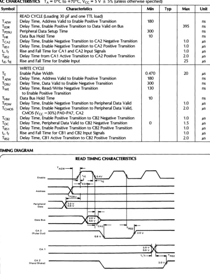
CLOCK TIMING- 6502, 03, 04, 05, 06
00 (IN)
~T<00
V,::_O \
O.4V- - -
~-P-W-H-0-0-L---.J
..I..
PWH00H--J '-.
_....:.'-'!4..:..V _ _ _ _2.4 V
_
f-
1.5V=\:._~/
,
~
PW H01---l '\
.4 V
,
,
R/W
CLOCK TIMING- 6512, 13, 14, 15
_ AEF"A"
1TD
1lvcc,
o.~vI
O.2V. . . - REF "s"
TIMING FOR READ!NG DATA FROM
MEMORY OR PERIPHERALS
\---REF "AU
.4V
--REF "B"
ADDRESS FROM MPU DATA FROM MEMORY ROY. S. 0 SYNC
0oClN)
0, (OUT)
TIMING FOR WRITING DATA TO
MEMORY OR PERIPHERALS
.4 V
~5V
~--"5V
- \'t-["""'4'-':-E-F-"A-.-.--'-·4'-V-'I',J:-:F~.:~·2 ~
'---NOTE
1 MHz TIMING
CLOCK nMING- 6512, 13, 14, 15
Symbol
Characteristic
Min
Typ
Max
Unit
Tcyc Cycle Time 1000 nsec
PWHI{>1 Clock Pulse Width I{> 1 430
PWHI{>2 (Measured at V cc - 0.2 V) 1{>2 470 nsec
TF Fall Time (Measured from 0.2 V to Vcc - 0.2 V) 25 nsec
To Delay Time Between Clocks (Measured at 0.2 V) 0 nsec
CLOCK nMING- 6502, 03, 04, OS, 06
Symbol
Characteristic
Min
Typ
Max
Unit
TCYC Cycle Time 1000 ns
PWHl{>o I{>o (IN) Pulse Width (measured at 1.5 V) 460 520 ns TRl{>o' TFl{>o I{>o (IN) Rise, Fall Time 10 ns
To Delay Time Between Clocks (measured at 1.5 V) 5 ns
PWHI{>1 1{>1 (OUT) Pulse Width (measured at 1.5 V) PWHl{>oL-20 PWHl{>oL ns PWHI{>2 1{>1 (OUT) Pulse Width (measured at 1.5 V) PWHl{>oH-40 PWHl{>oH-10 ns TR, TF 1{>1 (OUT). 1{>2 (OUT) Rise, Fall Time 25 ns
(measured .8 V to 2.0 V) (Load
=
30pF+
1 TTL)READIWRITE nMING
Symbol
Characteristic
Min
Typ
Max
Unit
TRws Read/Write Setup Time From MCS6500 100 300 ns
TAOS Address Setup Time From MCS6500 100 300 ns
TACC Memory Read Access Time 575 ns
Tosu Data Stability Time Period 100 ns
THR Data Hold Time - Read 10 ns
THW Data Hold Time - Write 30 60 ns
TMos Data Setup Time From MCS6500 150 200 ns
TROY RDY, S.O. Setup Time 100 ns
TSYNC SYNC Setup Time From MCS6500 350 ns
THA Address Hold Time 30 60 ns
2 MHz TIMING
CLOCK TIMING-
6512, 13, 14, 15, 16
Symbol
Characteristic
Min
Typ
Max
Unit
Tcyc Cycle Time 500 nsec
PWHt/l1 Clock Pulse Width 1/>1 215
PWHt/l2 (Measured at V cc - 0.2 V) 1/>2 235 nsec
TF Fall Time (Measured from 0.2 V to Vcc - 0.2 V) 12 nsec
To Delay Time Between Clocks (Measured at 0.2 V) 0 nsec
CLOCK TlMING-
6502,03,04,05,
06
Symbol
Characteristic
Min
Typ
Max
Unit
Tcyc Cycle Time 500 ns
PWHt/lo t/lo (IN) Pulse Width (measured at 1.5
V)
240 260 nsTRt/lo' TFI/>o t/lo (IN) Rise, Fall Time 10 ns
To Delay Time Between Clocks (measured at 1.5 V) 5 ns
PWHt/l1 t/l1 (OUT) Pulse Width (measured at 1.5
V)
PWHt/lol-20 PWHt/lol ns PWHt/l2 t/l2 (OUT) Pulse Width (measured at 1.5 V) PWHt/loH-40 PWHt/loH-10 nsT
R, TF t/l1 (OUT). t/l2 (oun Rise, Fall Time 25 ns(measured .8 V to 2.0 V) (Load
=
30pF+
1 TTL)READIWRITE TIMING
Symbol
Characteristic
Min
Typ
MaxUnit
TRWS Read/Write Setup Time From 6500A 100 150 ns
TAOS Address Setup Time From 6500A 100 150 ns
TACC Memory Read Access Time 300 ns
Tosu Data Stability Time Period 50 ns
THR Data Hold Time - Read 10 ns
THW Data Hold Time - Write 30 60 ns
TMDS Data Setup Time From 6500A 75 100 ns
TROY RDY, S.O. Setup Time 50 ns
TSYNC SYNC Setup Time From 6500A 175 ns
THA Address Hold Time 30
60
nsTHRW R/W Hold Time 30 60 ns
(40 Pin Package) Y" ROY "'I (OUT) IRQ N.C NMI SYNC Yee ABO
A B I
AB2 AB3 AB4 AB5 AB6 AB7 ABB AB9 ABIO ABII
(28 Pin Package)
RES
Vss
IRQ -
NMIVee
- ABOAB I -AB2 AB3- AB4AB5 AB6 AB7 ABS
-(28 Pin Package)
RES
Vss
IRQ
Vee
- ABOAB I AB2 - AB3AB4 AB5 AB6 - AB7- AS8AB9
-6502 I 40 2 39 3 38 4 37 5 36 6 35 7 34 8 33 9 32 10 31 II 301-12 29 13 28 14 27 15 26 16 25 17 24 18 23 19 22 20 21
6503
I 28 2 27 3 26 4 25 5 24 6 23 7 22 8 21 9 20 10 19 II 18 12 17 13 16
RES
"'2lO UT)
S.O.
"'O(IN)
N.C.
N. C. R/W DBO OBI
o B2 DB3 DB4 DB5 DB6 DB7 ABI5 ABI4 ABI3 ABI2 Yss t-- Q!2(OUT)
t--Q!O( IN)
t-- R/W
I-DBO
I-DB I
t-- DB2
t-- DB3
I- DB4
t-- DB5 I- D B6 t-- DB7
I-ABII t--ABIO
FEATURES
• 65K Addressable Bytes of Memory • IRQ Interrupt
• NMI Interrupt • On-the-chip Clock
... TTL Level Single Phase Input ... RC Time Base Input ... Crystal Time Base Input • SYNC Signal
(can be used for single instruction execution) • ROY Signal
(can be used for single cycle execution)
• Two Phase Output Clock for Timing of Support Chips
FEATURES
• 4K Addressable Bytes of Memory (ABOO-AB11) • On-the-chip Clock
• IRQ Interrupt • NMI Interrupt
• 8 Bit Hi-Directional Data Bus
14 151-AB9
6504
I 28 I-Q!2(OUT) 2 27 -Q!O(IN) 3 26 - R/W
4 25 - DBO
0 24 - DBI FEATURES 6 23 - DB2
• 8K Addressable Bytes of Memory (ABOO-AB12)
7 22 - DB3
• On-the-chip Clock
S 21 - DB4
• IRQ Interrupt
9 20 - D85
10 19 - DB6 • 8 Bit Bi-Directional Data Bus II 18 - DB7
(28 Pin Package)
RES
Vss
RDY IRQ
Vee
ABO -AB 1- AB2AB3 - AB4AB5 AB6 - AB7AB8
-(28 Pin Package)
RES
Vss
-QJI (OUT)IRQ
Vee
- ABOABI - AB2- AB3- AB4- AB5-ABS AB7-AB
8-(28 Pin Package)
RES
vss
vee
AO A1 A2 A3 A4 AS A6 A7 A8 All 6505I 28
2 27
3 26
4 25
5 24
6 23
7 22
8 21
9 20
10 19 II 18 12 17 13 16 14 15
6S06
I 28
2 27
3 26
4 25
5 24
6 23
7 22
8 21
9 20
10 19 II 18 12 17 13 16 14 15
6507 I- 02(OUT) I-IIJO(IN) I- R/W I-DBO I- DBI I- D B2 I- DB3 I- DB4 I-DB5 I- DB6 I- DB7 - ABII ... ABIO
I-AB9 I-02(OUT) 1-1IJ0(lN) I- R/W I-OBO I-OBI I-DB2 I-DB3 -DB4 I- DB5 I-DB6 I-DB7 I- ABII I-ABIO I- AB9 ~(OUT)
410 liN)
RIW
DO 01 02 03 04 05 06 07 A12 A1l Al0FEATURES
• 4K Addressable Bytes of Memory (ABOO-AB11)
• On-the-chip Clock
• IRQ Interrupt
• ROY Signal
• 8 Bit Bi-Directional Data Bus
FEATURES
• 4K Addressable Bytes of Memory (ABOO-AB11)
• On-the-chip Clock
• IRQ Interrupt
• Two phases off
• 8 Bit Bi-Directional Data Bus
FEATURES
• 81(
Addressable Bytes of Memory (AO-A 12)
• On-the-chip Clock
• ROY Signal
• 8 Bit Bi-Directional Data Bus
(40 Pin Package)
6512
Vss 40 RES ROY 2 39 021OUT)
01 3 38 5.0. IRQ - 4 37 02
Vss 5 36 DBE FEATURES
NMI - 6 35 N.C • 65K Addressable Bytes of Memory SYNC - 7 34 R/W
• IRQ Interrupt
Vee B 33 DBa
ABO 9 32 DB I • NMI Interrupt
ABI 10 31 DB2 • RDY Signal AB2 II 30 DB3
AB3 12 29 DB4 • 8 Bit Bi-Directional Data Bus AB4 13 28 DB5 • SYNC Signal
AB5 14 27 DB6 • Two phase input AB6 15 26 DB7
A B7- 16 25 ABI5 • Data Bus Enable AB8 17 24 ABI4
AB9 18 23 ABI3 ABIO 19 22 ABI2
ABII~ Vss
(28 Pin Package)
6513
Vss - I 28 f.- RES
01 - 2 27 '-- 02
IRQ - 3 26 - R/W
NMI - 4 25 - DBO
Vce - 5 24 I-DB I FEATURES
ABO- 6 23 I-DB2 • 4K Addressable Bytes of Memory (ABOO-AB11) AB I - 7 22 I- DB3 • Two phase clock input
AB2 - 8 21 DB4 • IRQ Interrupt AB3- 9 20 I- DB5 • NMI Interrupt
AB4- 10 19 I- DB 6 • 8 Bit Bi-Directional Data Bus AB5- II 18 I- DB7
(28 Pin Package)
6514
-Vss - I 28 f-RES
"'I - 2 27 I- "2
IRQ - 3 26 I-R/W
Vee - 4 25 I- DBO
ABO - 5 24 r- DB I FEATURES
ABI - 6 23 I- D B2 • UK Addressable Bytes of Memory (ABOO-AB12) AB2 - 7 22 I- DB3 • Two phase clock input
AB3 - 8 21 I- DB4 • IRQ Interrupt
AB4 - 9 20 I- DB5 • 8 Bit Bi-Directional Data Bus
AB5 - 10 19 I- DB 6 AB6 - II 18 I- DB7 AB7 - 12 17 I-ABI2 AB8 - 13 16 I-ABII AB9 - 14 15 I- AB 10
(28 Pin Package)
6515
Vss - I 28 .... RES
ROY - 2 27 - 02
01 - 3 26 - R/W
IRQ - 4 25 - DBO
Vee - 5 24 - DBI FEATURES
ABO - 6 23 - DB2 • 4K Addressable Bytes of Memory (ABOO-AB11)
ABI - 7 22 - DB3 • Two phase clock input AB2 - 8 21 - DB4 • IRQ Interrupt
AB3 - 9 20 -, D B5 • 8 Bit Bi-Directional Data Bus
NMOS
6500/1
One-Chip 8-Bit Microcomputer
• Single +5 Volt Power Supply.
• 2048 Bytes of ROM.
• 64
Bytes of RAM.• 32 Bi-Directionall/O Lines.
• 16-Bit Programmable Interval Timer/Event Counter. • Software-Compatible with MCS6502.
Description
• Pipeline Architecture for High-Performance. • Thirteen Address Modes With True Indexing
Capability.
• Variable Length Stack. • Two Index Registers.
The 6500/1 is a completely self-contained single-chip microcomputer system. Included in the 6500/1 are 2048 bytes of mask-programmable ROM, 64 bytes of RAM, 321/0 lines, a 16-bit timer/counter, and an on-chip clock oscillator. The internal processor architecture is identical to the 6502 to provide software compatibility and to assure high-performance operation.
PIN CONFIGURATION
Note
vee (RAM)
P07 POG POs P04 P03 PO, PO, POo XTI XTO GNO PC7 PCG PCs PC4 PC3 PC, PC, PCo
MCS = Ceramic package MPS = Plastic package
NMI RES PAo PAl PA, PA3 PA4 PAs PAG PA7 Vee PBo PB, PB, PB3 PB4 PBs PBG PB7 CNTR BLOCK DIAGRAM
IRQ I
I I I I I I I I I ~ I I I I L _ 2-15 I---XTO CLOCK OSCILLATION 32 I/O LINES I----XTI
1 - - - -Vee (RAM)
1 - - - -CNTR
INTERNAL ARCHITECTURE Index Registers
There are
two
8-bit index registers (X and V), which may be used to count program steps or to provide an index value to be used in generating an effective address. When executing an instruction which specifies indexed addressing, the CPU fetches the op code and the base address, and modifies the address by adding the index register to it prior to performing the desired operation. Indexing simplifies many types of programs, especially those which make extensive use of tables.Stack Pointer
The Stack Pointer is an 8-bit register used to control the addressing of the variable-length Stack. It is automatically decremented and incremented by the CPU when the Stack is accessed.
The Stack is used automatically by the CPU for interrupt processing and subroutine calling and may also be used by the programmer for other temporary storage functions.
Arithmetic and Logic Unit (ALU)
All arithmetic and logical operations are done in the ALU. The ALU has no internal memory and is used only to perform transient numerical operations.
Accumulator
The Accumulator is a special-purpose 8-bit register which is used to hold the results of most arithmetic and logical operations.
Program Counter
The 16-bit Program Counter provides the addresses which step the processor through sequential instructions in a pro-gram. Each time the processor fetches an instruction from program memory, the lower byte of the Program Counter (PCL) is placed on the low-order bits of the Address Bus and the higher byte of the Program Counter (PCH) is placed on the high-order 8 bits. The Counter is incre-mented each time an instruction or data is fetched from program memory.
Instruction Register and Instruction Decode
Instructions are fetched from ROM or RAM and gated onto the internal data bus. These instructions are latched
2-16
into the Instruction Register then decoded along with tim-ing and interrupt signals to generate control signals for the various registers.
Timing Control
The Timing Control Unit keeps track of the instruction cycle being executed. This unit is set to To each time an instruction fetch is executed and is advanced at the begin-ning of each Phase One clock pulse for as many cycles as are required to complete the instruction. Each data trans-fer which takes place between the registers depends on decoding the contents of both the instruction register and timing control unit.
Interrupt Logic
The interrupt logic controls the processor interface to the interrupt inputs to ensure proper timing, enabling and sequencing of the interrupt signals which the processor recognizes and services.
Clock Oscillator
The Clock Oscillator provides all the timing signals used by the CPU. A 2MHz crystal must be used with the 1MHz MCS6500/1 and a 4MHz crystal for the 2MHz MCS65OO/1A.
21< x 0 ROM
The 2048-byte Read Only Memory (ROM) usually contains the program instructions and other fixed data. These pro-gram instructions and constants are permanently stored in the ROM by metal mask programming during fabrication of the 6500/1.
64xORAM
The 64-byte Random Access Memory (RAM) contains the user program stack and is used as scratchpad memory. This RAM is completely static, requiring no clock or dy-namic refresh. A standby power pin allows RAM memory to be maintained at a reduced operating power. In the event that power is lost and execution stops, this standby power retains RAM data until execution resumes.
Status/Control Register
Counter/Latch ABSOLUTE MAXIMUM RATINGS
The Counter/Latch consists of a bit counter and a 16-bit latch register. The counter contains either a count of cb2 clock periods or a selected external event, depending on the counter mode selected in the Status/Control Register. The counter initialization value is stored in the latch.
Input/Output (I/O) Ports
The 6500/1 provides four 8-bit I/O ports-PA, PB, PC, and PD. The 321/0 lines of these ports are bidirectional; all signals may be used for either input or output.
INSTRUCTION SET
Rating
Supply Voltage
Input/Output Voltage
Operating Temp. Storage Temp.
Note
Symbol
Vee
VIN
Top TSTG
Allowable Range Unit
-0.3 to
+7.0 V
-0.3 to
+7.0 V
o
to 70 °C -55 to+150 °C
The 6500/1 instruction set is identical to that of the 6502
described in the preceding data sheet. All inputs contain protection circuitry to prevent damage due to static dis-charge. Care should be exercised to prevent unnecessary application of voltages in excess of the allowable limits.
COMMENT
Stresses above those listed under 'Absolute Maximum Rat-ings'may cause permanent damage to the device. These are stress ratings only. Functional operation of this device at these or any other conditions above those indicated in the operational sections of this specification is not implied and exposure to absolute maximum rating conditions for extended periods may affect device reliability.
DC ELECTRICAL CHARACTERISTICS (Vee
=
5.0V ±5%, TA=
D-70°C, unless otherwise noted)Symbol Parameter Min Typ
VIH Input High Voltage 2.0
VIL Input Low Voltage -0.3
VIHXT Input High Voltage (XTL 1) 2.4
VILXT Input Low Voltage (XTL 1) -0.3
liN Input Leakage (RES, NMI)
ITSI Three-State Input Leakage (PAo-PAl , PBo-PBl , PCO-PCl , PDo-PDl, CNTR), VIN
=
0.4 to 2.4VVOH Output High Voltage, ILOAD
=
100JlA 2.4VOl Output Low Voltage, ILOAD = 1.6mA
PD Power Dissipation
SOO
IRR Standby Current (RAM only) 10
CIN Input Capacitance (RES, NMI)
CTSI Three-State Input Capacitance (PAo-PAl , PBo-PBl , PCO-PCl , PDo-PDl, CNTR)
CINX Input Capacitance (XTL 1)
COUT Output Capacitance: V1N = OV, TA
=
25°C, f=
1.0 MHzMax Unit
Vee V
0.8 V
Vee V
0.4 V
2.5 JlA
10.0 JlA
V
0.4 V
mW rnA
10.0 pF
10.0 pF
50.0 pF
NMOS
6508
Microprocessor With RAM and
1/0
• 8-Bit Bi-directional 1/0 Port • Variable length stack • 256 Bytes fully Static RAM (internal) • Interrupt capability • Single +5 volt supply • 8 BIT Bi-directional Data Bus
• N channel, silicon gate, depletion load technology • Addressable memory range of up to 65K bytes • Eight bit parallel processing • Direct memory access capability
• 56 Instructions • Bus compatible with M6800 • Decimal and binary arithmetic • Pipeline architecture • Thirteen addressing modes • 1 MHz and 2 MHz operation
• True indexing capability • Use with any type or speed memory • Programmable stack pointer
DESCRIPTION
The 6508 is a low-cost microcomputer system capable of solving a broad range of small-systems and peripheral-control problems at minimum cost to the user.
One full page (256 bytes) of RAM is located (on chip) concurrently at Page 0 and Page 1, allowing Zero Page Addressing and stack operations with no additional RAM.
PIN CONFIGURATION BLOCK DIAGRAM
~n
6508
P,
AEC
RES 40 0, IN
0, IN 39 RIW
iRQ 38 DB.
AEC 37 DB,
VDD 5 36 DB, A,
A. 6 35 DB, A,
A, 7 34 DB. A,
A, 8 33 DB.
A, 9 32 DB. A,
A. 10 31 DB, A. 0:
W
A. 11 30 p. A, LL
LL
A. 12 29 p, =>
A, CIl INSTRUCTION
en DECODE
A, 13 28 p, en
A, w
A. 14 27 p, 0:
C>
A. 15 26 p. C>
A. «
A .. 16 25 p. w ~
A .. 17 24 p. A.
~
Au 18 23 p,
A" 0: w
Au 19 22 A .. J:
A"
I-VSS 20 21 A ..
An Au A" A"
OJ
0, 0, fi"SBITLINE 0, 0, DATA BUS
0,
DESCRIPTION (cont.)
An 8-bit Bi-Directionall/O Port is located on-chip with the Output Register at Address 0 0 0 1 and the Data-Direction Register at Address 0 0 0 0. The 1/0 Port is bit-by-bit programmable.
The Three-State sixteen-bit Address Bus allows Direct Memory Accessing (DMA) and multi-processor systems sharing a common memory.
The internal processor architecture is identical to the 6502 to provide software compatibility.
ABSOLUTE MAXIMUM RATINGS
Parameter
Symbol
Supply Voltage Vee
Input Voltage Yin
Operating Temperature
Range TA
Storage Temperature
Range TSls
Value
-0.3 to +7.0 -0.3 to +7.0
o
to +70-55 to +150
Unit
Vdc Vdc °C °C
COMMENT
This device contains input protection against damage due
to high static voltages or electric fields; however,
precau-tions should be taken to avoid application of voltages
higher than the maximum rating.
ELECTRICAL CHARACTERISTICS
(Vee = 5.0 V±
5%, Vss = 0, TA =0° to +70oq
Symbol
Parameter
Min
Typ
Max
Unit
VIH Input High Voltage
tP1,
tP2(in) Vee - 0.2 Vee + 1.0 V VdcInput High Voltage
RES, PO-P7 IRQ, Data Vss + 2.0 Vdc
VIL Input low Voltage
P.J:..
tP2(in) Vss - 0.3 Vss + 0.2 VdcRES, PO-P7 IRQ, Data Vss + 0.8 Vdc
liN Input leakage Current (VIN = 0 to 5.25 V, Vee = 5.25 V)
logic 2.5 /LA
tP1,
tP2(in) 100 /LAITSI Three State (Off State) Input Current
(VIN = 0.4 to 2.4 V, Vee = 5.25 V) 10 /LA
Data lines
VOH Output High Voltage
(IOH = -100 /LAdc, Vee = 4.75 V)
Data, AO-A 15,
R/W,
PO-P7 Vss + 2.4 VdcVOL Out low Voltage
(IOL = 1.6 mAdc, Vee = 4.75 V)
Data, AO-A 15,
R/W,
PO-P7 Vss + 0.4 VdcPD Power Dissipation W
C Capacitance pF
(VIN = 0, TA = 25°C, f = 1 MHz)
CIN logic, PO-P7 10
Data 15
COUT AO-A15,
R/W
12C"'1
tP1
30 50C"'2
tP2
50 80TIMING DIAGRAMS
0,(in)
0.{in) AIW ADDRESS FROM MPU
DATA
FROM
MEMORY
PERIPHER
DATA ADDRESS ENABLE CONTROL
CLOCK TIMING
TIMING FOR READING DATA FROM
MEMORY OR PERIPHERALS
~---_ _ _ _ _ _ _ _ _ Teye _ _ _ _ _ _ _ _ _ _ _ - . j
~--_ PWH0, - - - . j vee -O,2V
~T D 1 " - TD
f---", vee - D.2V I
1\
I/
:=-ffl"O~
\
I I I
--.
TF*
I--.
TAI~TAWS
THAW
-I
2.0VTHA - - .
~
2.0Va.8V
-
TAOS-
---
TAEW -TeOR.1
2.ov7
O.8V
~
TAce T TOSU
I--
- TpDSU ALX
~.~
~vee-D.2V
2-20
VCC-O.2V
i-~
-.-x==
i'..
V
TIMING DIAGRAMS
(cant.)CLOCK TIMING
TIMING FOR WRITING DATA TO
MEMORY OR PERIPHERALS
~ ____________________ ~TCYC ______________________ ~
~ ________ PWH0,
---'J.--II
vee -O.2V 0,(jn) _ _ _ ...;;;r
0. (in)
RIW ADDRESS FROM MPU
DATA FROM MEMORY PERIPHERA DATA
ADDRESS ENABLE CONTROL
~ TO ~
- - , VCC-02V 1
1\:
- . - O.2V I-
TF - IL
TAWS
\
~O.8VTAEW TWE
)<
- 2.0Va.BV
TAOS
~
f-VCC 02V
To
I-~
r-V
1\
-'" ~PWH0, _ _ -',=
-
TR+-~
2.0V
r--J
08~
~TMOS _ _
VCC-O.2V
1 1
'"
V
THW
~
TpDW
)<r-AC ELECTRICAL CHAR)<r-ACTERISTICS (Vee
=
5
V±
5%,
Vss=
0
V, TA=
OO-70
oq
1
MHz Timing
2 MHz Timing
Symbol
Parameter
Min
Typ
Max
Min
Typ
Max
Units
Clock Timing
Cycle Time
1000
500
nsTeye
PWH"'l Clock Pulse Width
cPl
430
215
nsPWH"'2 (Measured at Vee -
0.2
V)cP2
470
235
nsTF, TR Fall Time, Rise Time
25
15
ns(Measured from
0.2
V to Vee -0.2
V)To Delay Time between Clocks
0
0
ns(Measured at
0.2
V)READ/WRITE TIMING (LOAD = 1 TTL)
Symbol
Parameter
Min
Typ
Max
Min
Typ
Max
Units
TRws Read/Write Setup Time from
6508
100
300
100
150
nsTAOS Address Setup Time from
6508
100
300
100
150
nsTAee Memory Read Access Time
575
300
nsTosu Data Stability Time Period
100
50
nsTHR Data Hold Time - Read ns
THW Data Hold Time - Write
10
30
10
30
nsTMos Data Setup Time from
6508
150
200
75
100
nsTHA Address Hold Time
10
30
10
30
nsTHRW R/W Hold Time
10
30
10
30
nsTAEw Delay Time, Address valid to
180
nscP2
positive transitionTEDR Delay Time,
cP2
positive transition to395
nsData valid on bus
Tosu Delay Time, Data valid to
300
nscP2
negative transitionTWE Delay Time, R/W negative transition to
130
nscP2
positive transitionTpDw Delay Time,
cP2
negative transition to1
JJ,sPeripheral Data valid
TpDsu Peripheral Data Setup Time
300
nsSIGNAL DESCRIPTION Clocks
«P"
<P2)The 6508 requires a two phase non-overlapping clock that runs at the Vee voltage level.
Address Bus (Ao-A1S)
These outputs are TTL compatible, capable of driving one standard TTL load and 130 pF.
Data Bus (Do-D7)
Eight pins are used for the data bus. This is a bi-directional bus, transferring data to and from the device and peripherals. The outputs are tri-state buffers capable of driving one standard TTL load and 130 pF.
Reset
This input is used to reset or start the microprocessor from a power down condition. During the time that this line is held low, writing to or from the microprocessor is inhib-ited. When a positive edge is detected on the input, the microprocessor will immediately begin the reset sequence. After a system initialization time of six clock cycles, the mask interrupt flag will be set and the microprocessor will load the program counter from the memory vector loca-tions FFFC and FFFD. This is the start location for program control.
After Vee reaches 4.75 volts in a power up routine, reset must be held low for at least two clock cycles. At this time the R/W signal will become valid.
When the reset signal goes high following these two clock cycles, the microprocessor will proceed with the normal reset procedure detailed above.
Interrupt Request (IRQ)
This TTL level input requests that an interrupt sequence begin within the microprocessor. The microprocessor will complete the current instruction being executed before recognizing the request. At that time, the interrupt mask bit in the Status Code Register will be examined. If the interrupt mask flag is not set, the microprocessor will begin an interrupt sequence. The Program Counter and Proces-sor Status Register are stored in the stack. The micro-processor will then set the interrupt mask flag high so that no further interrupts may occur. At the end of this cycle, the program counter low will be loaded from address FFFE, and program counter high from location FFFF, therefore transferring program control to the memory vector lo-cated at these addresses.
Address Enable Control (AEC)
The Address Bus is valid only when the Address Enable Control line is high. When low, the Address Bus is in a high-impedance state. This feature allows easy DMA and multiprocessor systems.
I/O Port (Po-P7)
Eight pins are used for the peripheral port, which can transfer data to or from peripheral devices. The Output Register is located in RAM at Address 0 0 0 1, and the Data Direction Register is at Address 0 0 0 0. The outputs are capable at driving one standard TTL load and 130 pF. Read/Write (R/W)
This signal is generated by the microprocessor to control the direction of data transfers on the Data Bus. This line is high except when the microprocessor is writing to mem-oryor a peripheral device.
NOTE
The 6508 economizes on chip area by locating Page Zero and Page One concurrently in the same 256 bytes of RAM. This allows Page Zero addressing. with stack operations in Page One. with only 256 bytes of memory on-chip, resulting in lower chip area and hence, cost. During the initialization sequence, the stack pointer should be started at location 01FF. When talking to internal RAM, the Data Bus is in a high-impedance state.
ADDRESSING MODES Accumulator Addressing
This form of addressing is represented with a one byte instruction, implying an operation on the accumulator. Immediate Addressing
In immediate addressing, the operand is contained in the second byte of the instruction, with no further memory addressing required.
Absolute Addressing
In absolute addressing, the second byte of the instruction specifies the eight low order bits of the effective address while the third byte specifies the eight high order bits. Thus, the absolute addressing mode allows access to the entire 65K bytes of addressable memory.
Zero Page Addressing
The zero page instructions allow for shorter code and execution times by only fetching the second byte of the instruction and assuming a zero high address byte. Careful use of the zero page can result in significant increase in code efficiency.
Indexed Zero Page Addressing
(X, Y indexing) - This form of addressing is used in con-.junction with the index register and is referred to as 'Zero