•
•
8-Channel Programmable
Interface
Manual
Copyright
©
June I 1983• •
Contents
SECTION 1 - GENERAL INFORMATION 1 .1 INTRODUCTION
1 .2 GENERAL DESCRIPTION 1 .3 FEATURES
1 .4 SPECIFICATIONS
SECTION 2 - INSTALLATION
2.1 2.2 2.3 2.4
2.5
2.62.7
2.8 2.9 2.10UNPACKING AND INSPECTION ADDRESS SELECTION
VECTOR SWITCH SELECTION BAUD RATE SELECTION
LINE PARAMETERS SWITCH SELECTION CONSOLE SELECTION
BREAK RESPONSE CABLING
MODULE INSTALLATION
RACKMOUNT PANEL (OPTION)
SECTION 3 - PROGRAMMING CONSIDERATIONS 3.1 INTRODUCTION
3.2 DEVICE ADDRESS FORMAT 3.3 VECTOR INTERRUPT FORMAT 3.4 WORD FORMATS
3.3.1 Receive Control/Status Register (RCSR) 3.4.2 Receive Buffer (RBUF) 3.4.3 Transmit Control/Status
Register (XCSR) 3.4.4 Transmit Buffer (XBUF)
APPENDIX A BUS SIGNALS AND PIN ASSIGNMENTS
June 9, 1983
Figures
2-1 COMPONENT LOCATIONS SHOWING FACTORY CONFIGURATIONS
2-2 RACKMOUNT CONNECTOR PANEL
Tables
June 9, 1983
6
12
2-1 EXAMPLE ADDRESS SELECTION 7
2-2 VECTOR SELECTION EXAMPLES 8
2-3 BAUD RATE SELECTION 9
2-4 LINE PARAMETERS SWITCH SELECTION 10
2-5 CONSOLE ENABLE 10
2-6 BREAK RESPONSE 11
2-7 CABLE PIN ASSIGNMENTS 11
3-1 STANDARD ADDRESS AND VECTOR ASSIGNMENTS 14
..
.
Section, 1 - General Description
1.1 INTRODUCTION
This manual supplies the information needed to install and operate the SCD-DLV11J/8 8-channel serial line interface module manufactu-red by Sigma Information Systems, Anaheim, California. The material is arranged into the following sections:
SECTION 1 - GENERAL INFORMATION. This section contains a general description of the interface module, along with features. Spec-ifications are included.
SECTION 2 - INSTALLATION. This section contains the switch selection and associated register formats for device and vector address assignments, baud rates and line parameters. Cabling and backplane installation is included.
SECTION 3 - PROGRAMMING CONSIDERATIxJNS. This section contains the address/vector formats and register formats for transmit and re-ceive control/status and buffer registers.
1.2 GENERAL DESCRIPTION
June 9, 1983 Page 2
The SCD-DLV11J/8 is a dual-wide asynchronous interface between the LSI-11 bus and up to eight standard serial I/O devices. It is software compatible with DEC* operating systems and diagnostics designed for the DLV11J. It plugs directly into any dual Q bus* slot.
Sigms's SCD-DLV11J/8 has switch selectable address (160000 to 177776) and vector (000 to 776) assignments. Once the initial ad-dress and vector are assigned, all eight channels are contiguous except the console channel which, if selected, resides at 177560 with vector at 60.
All channels share a programmable baud rate with a switch select-able default value. Baud rates range from 50 to 19.2K buad. The SCD-DLV11J/8 supports only RS-232C devices with all channels shar-ing switch selectable line parameters.
The interface module includes two 12-foot, 4-channel cables, each with four DB25P connectors. An optional rackmount panel provides convenient mounting for the eight DB25P connectors.
1.3 FEATURES
The following are some of the features of the SCD-DLV11J/8P.
• Eight asynchronous serial lines can be supported on one dual-wide module.
• The module is plug compatible with LSI-11 backplanes and plugs directly into any Q bus slot without backplane modification.
• The interface is software compatible with operating systems and diagnostics designed for the DLV11J.
• Baud rate is programmable with a switch selectable default value.
• Device address and vector assignments are switch selectable.
• Line parameters are switch selectable.
*DEC and Q bus are registered trademarks of Digital Equipment Cor-poration.
•
1.4 SPECIFICATIONS
Power Requirements:
Device Address:
Vector
Baud Rate:
Line Parameters:
Data Bit: Parity: Stop Bit:
Operation:
I nterface Type:
Bus Load:
Cables:
Optional Panel:
Installation: Dimensions: Temperature Operating: Storage: Humidity:
June 10, 1983 Page 3
+5VDC AT 2.0A 12VDC at 0.2A
Switch selectable 160000-177776 (Console
=
171560)Switch selectable 000-776 (console
=
60)Programmable per channel
50, 75, 110, 1 34 .5, 1 50, 200, 300, 600, 1200, 1800, 3400, 3600, 4800 7200, 9600 and 19.2K
Switch selectable. Shared by all channels
7 or 8
Odd, even or none
1 or 2
Full duplex
RS-232C
One DC load
Includes two 12-ft, 4-channel cables, each with four DB25P connectors.
Terminals require null modem cables with DB25S connectors to SCD-DLV11J/8P and associated terminal connectors.
Mounts the eight DB25P connectors for convenient rear rackmount cabling to RS-232C devices.
Plugs directly into any standard Q bus slot that provides continuous BIAK1 and BlAKO lines.
Single dual-wide module: 5.2"W x 8.9"H (13.2cmW x 22.8cmH)
oOC to 50°C -40°C to 85°C
10% to 90% noncondensing
-June 10, 1983 Page
4
.'
..
Section 2 - Installation
June 10, 1983 Page 5
2.1 UNPACKING AND INSPECTION
The SCD-DLV11J/8P is shipped in a special packing carton designed to keep the module from vibrating and to give it maximum protec-tion during shipment. The packing carton should be retained in case the unit requires reshipment.
Unpack the SCD-DLV11J/8P and visually inspect it for any damage that may have occurred during shipment. If any damage has oc-curred notify Sigma Information Systems immediately.
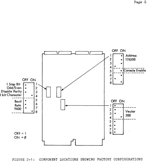
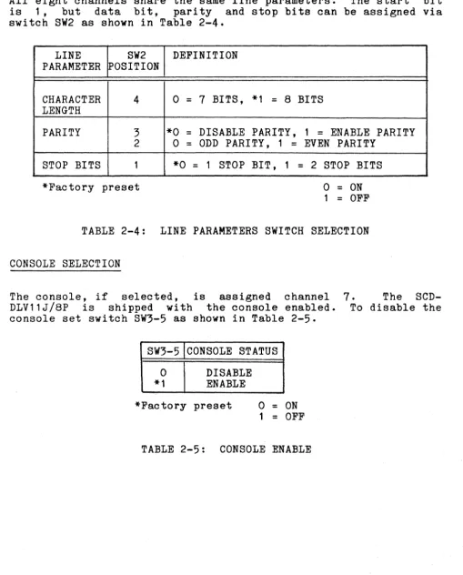
OFF ON
1 Stop Bit •
Odd/Even • Disable Parity • 8 bit Character
1
2 3 • 4
---.-
---Baud •
Rate • 9600 .• ,
OFF::::: 1 ON :::::¢
5
6 7
• 8
FIGURE 2-1 :
June 10, 1983 Page 6
OFF ON
1 • Address 2 • 176500
3 •
4 ~ ____________ _
5 ___ ~_~~~S~i!~~~~e
6 •
7 •
8'--_· ....
. OFF ON
~---4--1 •
---2 •
3 . Vector
4 • 300
---
---5 •
6 • 7 • 8 •
COMPONENT LOCATIONS SHOWING FACTORY CONFIGURATIONS
[image:10.615.39.571.46.599.2]..
June 9, 1983 Page 7
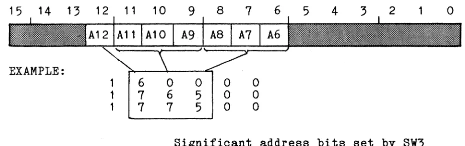
2.2 ADDRESS SELECTION
The SCD-DLV11J/8P has switch selectable device addressing in the range of 160000 to 177776 (octal). Once an initial address is as-signed, the remaining seven channels are contiguous except the console which, if selected, resides at 177560 as channel 7. Refer to Section 3.1 for a description of the device address and vector interrupt assignments. The initial address format is shown below.
15 14 13 12 11 10
EXAMPLE: 1 1 1 6 7 7
9
8
7
6 5 4 3 2a
a
0a
06 5
a
a
7 5 0 0
Significant address bits set by SW3
The initial address is determined with significant address bits A6-A12 set by switch SW3. Some examples follow in Table 2-1.
ADDRESS A12
SET BY
SW3 1
1 764 00 1
*1 765 00 1
1 766 00 1
*Factory preset
ADDRESS BITS A11 IA10
IA9 I
A8SW3- POSITIONS, 213141 8
1 1
a
11 1
a
11 1
a
1A7 A6.
7 6
0 0 0 1 1 0
o
= ON1
=
OFF [image:11.615.80.546.225.371.2]2.3 VECTOR SWITCH SELECTION
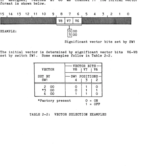
June 9, 1983 Page 8
The SCD-DLV11J/8P has switch selectable vector assignments in the range of 000-776 (octal). Once the initial vector is assigned the remaining seven vectors are contiguous except the console which, if assigned, resides at 60 as channel 7. The initial vector format is shown below.
15 14 13 12 11 10 9 8 7 6 5 4 3 2
o
EXAMPLE:
Significant vector bits set by SW1
The initial vector is determined by significant vector bits V6-V8 set by switch SW1. Some examples follow in Table 2-2.
---VECTOR BITS--VECTOR V8
I
V7I
V6SET BY --SW1
POSITIONS-SW1 4
I
3I
22 00 0 1 0
*3 00 0 1 1
6 00 1 1 0
*Factory present
o
=
ON1 = OFF
TABLE 2-2: VECTOR SELECTION EXAMPLES
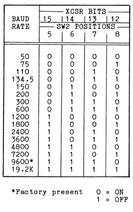
[image:12.615.57.544.177.751.2]2.4 BAUD RATE SELECTION
June 9, 1983 Page 9
All channels share the same programmable baud rate. The baud rate format is shown below.
15 14 13 12 11 10 9 8 7 6 5 4 3 2
o
where BRO-BR3 define programmable baud rates and SW2 defines de-fault switch selectable baud rates as shown in Table 2-3.
XCSR BITS BAUD 15 I 14 /13 I 12 RATE t - - SW2
POSITIONS-5
I
6J
7I
850 0 0 0 0
75 0 0 0 1
110 0 0 1 0
134.5 0 0 1 1
150 0 1 0 0
200 0 1 0 1
300 0 1 1 0
600 0 1 1 1
1200 1 0 0 0
1800 1 0 0 1
2400 1 0 1 0
3600 1 0 1 1
4800 1 1 0 0
7200 1 1 0 1
9600* 1 1 1 0
19.2K 1 1 1 1
*Factory present
o =
ON 1=
OFF [image:13.618.240.453.266.605.2]June 9, 1983 Page 10
2.5 LINE PARAMETERS SWITCH SELECTION
All eight channels share the same line parameters. The start bit is 1, but data bit, parity and stop bits can be assigned via switch SW2 as shown in Table 2-4.
LINE SW2 DEFINITION
PARAMETER ~OSITION
CHARACTER 4 0
=
7 BITS, *1=
8 BITS LENGTHPARITY 3 *0
=
DISABLE PARITY, 1=
ENABLE PARITY 2o
=
ODD PARITY, 1=
EVEN PARITYSTOP BITS 1 *0
=
1 STOP BIT, 1=
2 STOP BITS*Factory preset
o
=
ON1
=
OFFTABLE 2-4: LINE PARAMETERS SWITCH SELECTION
2.6 CONSOLE SELECTION
The console, if selected, is assigned channel
7.
The SCD-DLV11J/8P is shipped with the console enabled. To disable the console set switch SW3-5 as shown in Table 2-5.SW3-5 CONSOLE STATUS
0 DISABLE
*1 ENABLE
*Factory preset
o
=
ON 1=
OFFTABLE 2-5: CONSOLE ENABLE
----~---~---
[image:14.617.51.561.123.756.2]June 9, 1983 Page 11
2.7 BREAK RESPONSE
Channel 7 can be configured to either bootstrap, halt (console em-ulation mode), or have no response to a receive break condition. A bootstrap operation upon a receive break condition causes the CPU to execute the bootstrap program strating at the memory loc-ation defined by the power-up mode jumpers of the CPU. A halt operation unpon a receive break condition causes the processor to halt and the console octal debugging technique (ODT) microcode to be invoked. Configurations are shown in Table 2-6.
BREAK RESPONSE E1-E2 E1-E3
None OUT OUT
Boot IN OUT
Halt OUT IN
TABLE 2-6: BREAK CONFIGURATIONS
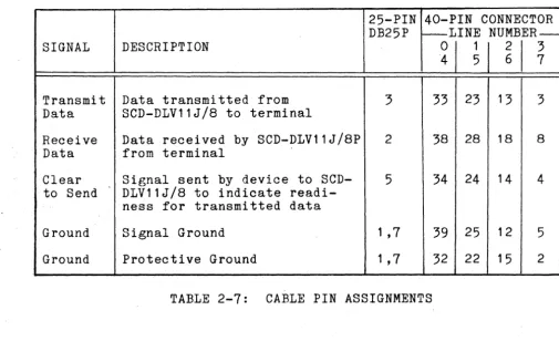
2.8 CABLING
The SCD-DLV11J/8P has two 40-pin connectors and is supplied with two cables, each terminating in four DB25P connectors. The 40-pin connectors and associated 25-pin terminating connector pin as-signments are defined in Table 2-6.
25-PIN 40-PIN CONNECTOR DB25P ~LINE NUMBER--SIGNAL DESCRIPTION
~I
~
I
~
I
3 7Transmit Data transmitted from 3 33 23 13 3
Data SCD-DLV11J/8 to terminal
Recei ve Data received by SCD-DLV11J/8P 2 38 28 18 8
Data from terminal
Clear Signal sent by device to SCD- 5 34 24 14 4 to Send DLV11J/8 to indicate
readi-ness for transmitted data
Ground Signal Ground 1 ,7 39 25 12 5
Ground Protective Ground 1 ,7 32 22 15 2
[image:15.618.51.569.57.417.2] [image:15.618.58.563.441.749.2]June 9, 1983 Page 12
The SCD-DLV11J/SP provides a Clear to Send input which can be driven by the attached serial line device to cause the SCD-DLV11J/SP channel to stop transmitting. The common use for this feature is with a printer that does not support XON-XOFF, but does provide a buffer full signal. This buffer status signal can be used to assert the CTS signal and effectively control transmission of data to the printer from the SCD-DLV11J/SP.
Cabling to terminals requires null modem cables with DB25S sockets between the SCD-DLV11J/SP connectors and associated terminal con-nectors.
2.9 MODULE INSTALLATION
The SCD-DLV11J/SP plugs directly into any Q bus slot, providing BIAK1 and BIAKO lines from the interface to the CPU are continu-ous. Bus signals and associated pin assignments are listed in Appendix A.
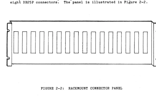
2.10 RACKMOUNT PANEL (OPTION)
An optional rackmount panel provides convenient mounting for the eight DB25P connectors. The panel is illustrated in Figure 2-2.
FIGURE 2-2: RACKMOUNT CONNECTOR PANEL
[image:16.621.40.565.394.730.2]Section 3 - Programming Considerations
3.1 INTRODUCTION
June 10, 1 9S3 Page 13
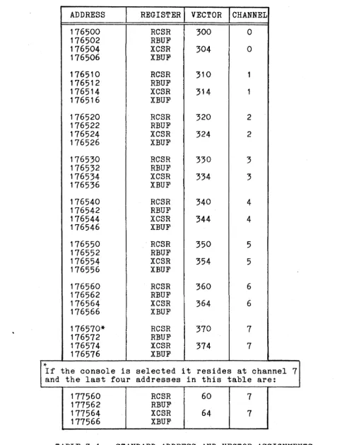
The SCD-DLV11J/SP is controlled by four device registers per chan-nel for a total of 32 device registers. The four device registers provided for each of the eight channels are:
RCSR RBUF XCSR XBUF
Receive Control/Status Registers Receive Buffer
Transmit Control/Status Register Transmit Buffer
ADDRESS 176500 176502 176504 176506 176510 176512 176514 176516 176520 176522 176524 176526 176530 176532 176534 176536 176540 176542 176544 176546 176550 176552 176554 176556 176560 176562 176564 176566 176570* 176572 176574 176576
*
If the console is and the last four177560 177562 177564 177566
REGISTER VECTOR CHANNEL
RCSR 300 0
RBUF
XCSR 304 0
XBUF
RCSR 310 1
RBUF
XCSR 314 1
XBUF
RCSR 320 2
RBUF
XCSR 324 2
XBUF
RCSR 330 3
RBUF
XCSR 334 3
XBUF
RCSR 340 4
RBUF
XCSR 344 4
XBUF
RCSR 350 5
RBUF
XCSR 354 5
XBUF
RCSR 360 6
RBUF
XCSR 364 6
XBUF
RCSR 370 7
RBUF
XCSR 374 7
XBUF
selected it resides at channel addresses in this table are:
RCSR 60 7
RBUF
XCSR 64 7
XBUF
June 10, 1983 Page 14
7
[image:18.615.46.524.76.706.2]3.2 DEVICE ADDRESS FORMAT
The address configurations are listed in Table 3-2.
17 16 15 14 13 12 11 10 9 8 7 6 5 4
I
1 1 1 1 I 1 IA12 All1Al0 IA9 A8 I A7 I A6 ...71
,
Bank
Selected (1 )
Initial Address (See Section 2.2)
Channel (Device) Select 000
=
cn
0001
=
CH 1 010=
CH 2 011=
CH 3 100=
CH 4 101=
CH 5 110=
CH 6 11 1=
CH 7Register Select 00
=
RCSR 01=
RBUF 10=
XCSR 1 1=
XBUFByte Pointer
June 9, 1983 Page 15
3 2
I
o
June 9, 1983 Page 16
3.3 VECTOR INTERRUPT FORMAT
The interrupt vector format is shown below.
17 16 15 14 13 12 11 10 9 8 7 6 5 4 3 2 1 0
V6
Initial Vector (See Section 2.3)
Channel Requesting Interrupt
000 = CH 0
001 = ClI 1
010 = CH 2
011 = CH 3
100
=
CH 4101 = CH 5
110
=
CH 6 111 = CH 7Interrupt ________________________________________________ ~
o
=
Receiver Interrupt 1=
Transmitter InterruptJune 10, 1983 Page 17
3.4
WORD FORMATSThe four word formats, one for each device register within a channel, are described in the following sections.
RX DN
RX INT
Receive Control/Status Register (RCSR)
12 11 10 8 7 6
RX RX
DN INT
RECEIVER DONE. Set when an entire character has been received and is ready for input to the CPU. Cleared when RBUF is read or BINIT L signal goes true. If RX INT (bit 6) is set, setting RX DN starts an interrupt sequence. Read only.
RECEIVER INTERRUPT ENABLE. Set under pro~ram control to generate a receiver interrupt request (when a char-acter is ready for input to the processor signified by bit 7 being set). Cleared under program control or by BINIT signal. Read/write.
June 10., 1983
Page 18
15
CH OVR ERR RUN
Receiver Buffer (RBUF)
7 6 5 4 3 2 1
DATA BITS
CH ERR CHANNEL ERROR STATUS. Logical OR of bits 14, 13, and 12. Read only.
OVR OVERRUN ERROR. When set, indicates that the reading RUN of the previously received character was not completed
(receiver done not cleared) prior to receiving a new character. Cleared by BINIT signal. Read only.
o
NOTE: When "back-to-back" characters are received, one full character time is allowed from the time instant
receiver done (bit 7) is set to the occurrence of an overrun error.
FRM FRAMING ERROR. When set, indicates that the character ERR read had no valid stop bit. Cleared by BINIT signal.
Read only.
PAR PARITY ERROR. When set, indicates that the parity
ERR received does not agree with the expected parity. This bit is always 0 if no-parity operation is configured for the channel. Read only.
NOTE: Error bits remain valid until the next character is received, at which time the error bits are updated.
DATA DATA BITS. Contains seven or eight data bits in a
BITS right-justified format. Bit
7
=
0 when7
data bits are enabled. Read only.All bits not used are read as O.
•
BR3-BRO
BR ENB
Transmit Control/Status Register (XCSR)
June 9, 1983 Page 19
PROGRAMMABLE BAUD RATE SELECT. When set, these bits choose a baud rate from 50-19.2K baud. See section 2.4. Write only.
PROGRAMMABLE BAUD RATE ENABLE. Must be set in order to select a new baud rate indicated by bits 12-15. Write only.
XMT TRANSMIT READY. Set when XBUF is empty and can accept RDY another character for transmission. It is also set by
INIT, during power-up or during a reset instruction. Read only.
XMT TRANSMIT INTERRUPT ENABLE. Set under program control INT when it is desired to generate a transmitter interrupt
request when transmitter is ready to accept a character for transmission. Cleared under pro~ram control, during power-up or reset instruction. Read/write.
XMT TRANSMIT BREAK. Set or reset under program control. BRK When set, a continuous space level is transmitted.
However, transmit done and transmit interrupt can still operate, allowing software timing of break. When not set, normal character transmission can occur. Cleared by BINIT. Read/write.
All bits not used are read as O.
3.4.4 Transmit Buffer (XBUF)
15 14 13 12 11 10 9 8 7 6 5 4 3 2
o
DATA BITSBits 0-7 contain the seven or eight right-justified data bits. Loaded under program control for serial transmission. Bits not used are read as O.
.~.---CONNECTOR A CONNECTOR B
PIN SIGNAL NAME PIN SIGNAL NAME
AAI Not Used BAI BDCOK H
ABI Not Used BBI Not Used
ACI Not Used BCI Not Used
ADI Not Used BDI Not Used
AEI Not Used BEl Not Used
AFI Not Used BFI Not Used
AHI Not Used BHl Not Used
AJI GND BJI GND
AKI Not Used BKI Not Used
ALI Not Used BLI Not Used
AMI GND BMI GND
ANI Not Used BNI Not Used
API BHALH BPI Not Used·
ARl Not Used BRI Not Used
ASI Not Used BSI Not Used
ATI GND BTl GND
AUl Not Used BUl Not Used
AVI Not Used BVl +5VDC
AA2 +5VDC BA2 +5VDC
AB2 Not Used BB2 Not Used
AC2 GND BC2 GND
AD2 +l2VDC BD2 Not Used
AE2 BOOUT L BE2 BDAL2 L
AF2 BRPLY L BF2 BDAL3 L
AH2 BDIN L BH2 BDAL4 L
AJ2 BSYNC L BJ2 BOAL5 L
AK2 Not Used BK2 BDAL6 L
AL2 BIRQL BL2 BDAL7 L
AM2 BIAKI L BM2 BDALS L
AN2 BIAKO L BN2 BDAL9 L
AP2 BBS7 L BP2 BDALlO L
AR2 BDMGI L BR2 BDALll L
AS2 BDMGO L BS2 BDALl2 L
AT2 BINIT L BT2 BDALl3 L
AU2 BDALO L BU2 BDALl4 L
AV2 BDALI L BV2 BDALl5 L