Anomalous
photovoltaic
effect
in
organic-inorganic
hybrid
perovskite
solar
cells
YongboYuan,1,2Tao Li,3 QiWang,1JieXing,1AlexeiGruverman,3Jinsong Huang1*
Organic-inorganichybridperovskites(OIHPs)havebeendemonstratedtobehighlysuccessfulphotovoltaicmaterials yieldingvery-high-efficiencysolarcells.Wereporttheroomtemperatureobservationofananomalousphotovoltaic (APV)effectinlateralstructureOIHPdevicesmanifestedbythedevice’sopen-circuitvoltage(VOC) that is much larger
thanthebandgapofOIHPs.ThepersistentVOCisproportionaltotheelectrodespacing,resemblingthatofferroelectric
photovoltaicdevices.However,theAPVeffectinOIHPdevicesisnotcausedbyferroelectricity.TheAPVeffectcanbe explainedbytheformationoftunnelingjunctionsrandomlydispersedinthepolycrystallinefilms,whichallowsthe accumulationofphotovoltageatamacroscopiclevel.Theformationofinternaltunnelingjunctionsasaresultofion migrationisvisualizedwithKelvinprobeforcemicroscopyscanning.Thisobservationpointsoutanewavenueforthe formationoflargeandcontinuouslytunableVOCwithoutbeinglimitedbythematerials’bandgap.
INTRODUCTION
Organic-inorganic hybrid perovskite (OIHP) materials have been revo-lutionizing the photovoltaics field in recent years with their use in high-efficiency solar cells (with power conversion high-efficiency exceeding 22%) and low-cost potential (1–10). Meanwhile, the development of other OIHP-based devices, such as lasers (11,12), high-gain photodetectors (13,14), light-emitting diodes (15), and transistors (16), is also in full swing. It is widely wondered whether OIHP materials will continue to generate breakthroughs in the optoelectronics field with their intriguing electronic and optoelectronic properties. Currently, there is a consensus that OIHP materials are a group of soft materials with high electronic and ionic conduction due to their relatively loosely bonded crystal structure (17–21). Investigations focused on making full use of this unusual property have been recently performed (22). In addition, a more insightful understanding of the photovoltaic process in OIHP materials is crucial to further improving the photocurrent and photo-voltage output of OIHP solar cells (23,24).
Here, we report the observation of an anomalous photovoltaic (APV) effect in lateral structure OIHP solar cells. Investigations focused on the APV effect in some inorganic materials, especially ferroelectrics, have attracted an upsurge in interest over the past decade because of its completely different working mechanisms and output characteristics compared to those of traditional p-n junction solar cells (25–29). To date, several semiquantitative or phenomenological models have been established to explain the APV effect, which can be classified into two major types: (i) the intrinsic noncentrosymmetry in bulk materials and (ii) the granularity of the polycrystalline materials (26,30,31). The former type of APV mechanism principally demands a very low con-ductivity in photovoltaic materials (25), whereas the latter mechanism does not suffer from a similar limitation. However, to date, most models for the granularity mechanism (for example, the Dember effect model, the structure transition model, and the p-n junction array model) are speculative because the corresponding formation mechanisms have not been proven. Hence, determining the origins of the open-circuit voltage
(VOC) that is larger than the materials’bandgap with experimental ev-idence is of great academic interest (25).
RESULTS
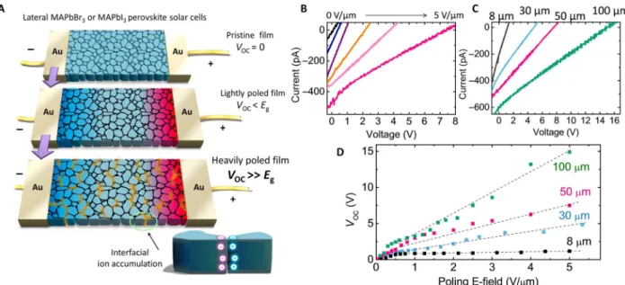
The OIHP solar cells used in this study had a symmetric lateral structure of Au/MAPbBr3(or MAPbI3and CsPbBr3)/Au, where the photoactive layer and metallic electrodes were deposited directly on a glass substrate (Fig. 1A). The as-made OIHP solar cells did not show any photovoltaic effect because of the symmetric lateral structure (17,19). After the lateral MAPbBr3device was electrically poled by a moderate electrical field of 0.3 to 0.5 V/mm at room temperature (RT) for 1 to 2 min, a largeVOCof about 1.1 to 1.3 V was obtained (Fig. 1A) from the MAPbBr3devices, with an electrode spacing of 50mm, which is close to the bestVOC(1.4 V) reported for vertical structure MAPbBr3solar cells (32,33). The gener-ation of this largeVOCin a device with symmetrical electrodes can be ascribed to the in situ formation of a p-i-n or p-n structure in the MAPbBr3film induced by ion migration and space-charge doping, as illustrated in Fig. 1A (middle) (19,33). The short-circuit current (ISC) is ~300 pA for devices with an active area of 50mm × 1 mm under an illumination intensity of 25 mW/cm2. The device’sVOCshowed a linear relationship with the poling bias, as shown in Fig. 1 (B and C). Aston-ishingly, when the lateral MAPbBr3device was poled by a larger elec-trical field of 5 V/mm for 1 to 2 min, theVOCfurther increased markedly to 7.4 eV, which is much larger than the bandgap (2.3 eV) of MAPbBr3. Meanwhile, the photocurrent increased slightly to 490 pA (Fig. 1B). In lateral devices with a MAPbI3photoactive layer, noVOClarger than the bandgap was observed at RT, which is consistent with our previous study (17,19). Nevertheless, a similar over-bandgapVOCof 2.6 V was observed when the poling temperature was elevated to be around 330 K (fig. S1). The anomalously largeVOCin the OIHP materials was found to increase with the spacing between the two electrodes (Fig. 1, C and D) when the poling electrical field was fixed at 5 V/mm. A largeVOCof 14.9 V was found in MAPbBr3solar cells with an electrode spacing of 100mm after an electrical poling at 5 V/mm for 1 to 2 min. There is a threshold at an electrode spacing of 8mm, below whichVOCexceeding the bandgap cannot be found, even at a high poling field of 5 V/mm.
This is the first time that OIHP solar cells with aVOClarger than the bandgap have been observed, which needs a mechanism for interpreta-tion. An APV effect dependent on electrode spacing has been frequently observed in some materials that lack a center of symmetry, generally 1Department of Mechanical and Materials Engineering, University of Nebraska–Lincoln,
Lincoln, NE 68588–0656, USA.2Hunan Key Laboratory of Super Microstructure and
Ultrafast Process, School of Physics and Electronics, Central South University, Changsha, Hunan 410083, P. R. China.3Department of Physics and Astronomy, University of
known as a bulk photovoltaic (BPV) effect due to the generation of “shift current”under illumination (30,34). The BPV effect has more frequently been observed in ferroelectric materials, which have an aligned internal field after poling (24,29). The ratio between the avail-ableVOCand the electrode spacing (0.1 to 0.2 V/mm) in OIHP is close to that of the BPV-based APV effect in some typical inorganic ferroelectric materials, such as bismuth ferrite (BFO; ~0.1 V/mm) and lanthanum-doped lead zirconate titanate (PLZT; ~0.2 V/mm) (25–27). However, MAPbBr3at RT has a cubic structure and thus does not meet the crystal structure for ferroelectricity. On the other hand, the ordering of polar organic cations, such as MA+, has been theoretically predicted to be the other route of polar domain formation (35,36). Nevertheless, many the-oretical and experimental studies indicate that MA+cations easily rotate in the inorganic cage at RT (37–40). The quick reorientation of the or-ganic cations was claimed to contribute to the dynamic screening of en-ergetic hot carriers in hybrid perovskites (41). On the experimental side, although switchable local phase contrast in PFM imaging of MAPbI3 films was observed, which, in principle, could be explained by the MA+ordering, no reliable hysteretic piezoresponse force microscopy (PFM) loop has been observed at RT in either single crystalline or poly-crystalline samples (42). To date, there is no solid experimental evidence to support the notion of ferroelectricity in MAPbI3despite speculations on the polar ordering in tetragonal MAPbI3at RT (20,43). Moreover, the anomalousVOChas only showed up in MAPbI3devices at an elevated poling temperature of around 330 K, which is also contrary to the ferroelectric mechanism because if ferroelectricity exists, then the spontaneous polarization should vanish above the phase transition temperature (330 K for MAPbI3). In addition, a dependence of the anomalousVOCon the polarization direction of the incident light is considered as a fingerprint of the BPV in ferroelectric materials (27). Here, the anomalousVOCobserved in OIHP materials did not respond to the light polarization direction change (fig. S2), which also excludes the contribution of the BPV effect. There was a new interesting mech-anism of photoferroelectricity [proposed by Liuet al.(44)] that suggests
light-induced ordering of MA+in MAPbI3, which could explain the ex-perimentally observed light-enhanced piezoelectricity (43). However, its contribution to the APV effect observed here can be excluded, because a similar above-bandgapVOC(for example, 5.9 V) can be obtained when the polar MA+in MAPbBr3was replaced by nonpolar Cs+cations (fig. S3). It has been established that ion migration occurs in OIHP materials under electric poling, which is responsible for the current hysteresis and many other unique properties of perovskite electronic devices (13,16–19,45–48). Ions may diffuse back after turning off the poling bias, which may also generate a current. It is thus necessary to find out whether the observedVOCis an artifact caused by the back diffusion of ions. Because the ion migration process is very sensitive to tempera-ture, freezing the ion migration at low temperature should exclude its contribution to the photocurrent.
The APV effect was studied for a large temperature range (from 120 to 330 K), as shown in Fig. 2 (A and B). The anomalously largeVOC remained (for example, 5.1 V) when the device was measured at a suf-ficiently low temperature of 120 K. The largeVOCwas obtained by scanning the device in both forward and backward directions (fig. S4). No hysteresis effect was observed in a wide temperature range of 120 to 330 K, which is consistent with our previous observation and excludes the contribution of ion redistribution to the photocurrent observed here. This can be explained by the fact that theI-V(current-voltage) curves scanned here only applied a small electrical field (0.1 V/mm) to the OIHP films and hence should not cause significant ion migration (19). TheISC lost nearly half of its value when the temperature decreased from 330 to 120 K, which can be explained by the more severe charge trapping effect at lower temperature. TypicalVOCenhancement at lower temperature due to the reduced saturated dark current was not observed here because the random (or noncontinuous) tunneling junction distribution results in the leakage current dominating the total dark current.
When the illumination light intensity changed, a semilogarithmic increase inVOCwith the photocurrentISCwas observed, that is,VOC¼
nkT
q ln ISCIo , wherekis the Boltzmann constant,Tis the temperature,qis
Fig. 1. APV effect in OIHP solar cells.(A) Scheme of the lateral perovskite solar cells before (top) and after electrical poling (middle and bottom), where the device structure is Au/MAPbBr3(or MAPbI3)/Au.Eg, bandgap. (B)I-Vcurves of the MAPbBr3devices after different intensities of electrical poling (for example, poling for 1 to 2 min at 0.2, 0.3, 0.8, 2, and
5 V/mm, respectively). (C)I-Vcurves of the electrically poled (5 V/mm) MAPbBr3devices with different electrode spacings. (D) SummarizedVOCof lateral MAPbBr3devices with
the unit charge, andnis the ideal factor (~31). This anomalousVOC variation behavior, with respect to the incident light intensity (Fig. 2C), also excludes ion back diffusion as the dominating contribution to the photocurrent because ion back diffusion current is sensitive only to poling bias and not to light intensity. Note that if theI-Vcurve scan is conducted immediately after the electrical poling, then there is an ion back diffu-sion current component added onto the photocurrent (Fig. 2D). Howev-er, its contribution quickly decreases after poling and becomes negligible after ~200 s, the time scale in which the photocurrent was measured for this project. On the other hand, the photocurrent generated by the APV effect was much more stable. Figure 2E shows that the photocurrent output of a MAPbBr3solar cell measured at a fixed voltage of 4 V can last for several hours. When stored in the dark, the electrically poled MAPbBr3solar cell can maintain its above-bandgapVOCovernight (fig. S5). The slow photocurrent decrease in the time scale of 1000 s (Fig. 2E) is attributed to the light-induced degradation of the perovskite film, because the uncovered MAPbI3(MAPbBr3) tends to lose methyl-ammonium and probably iodine much faster in vacuum and under il-lumination (see a demonstration in fig. S6).
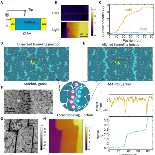
To further confirm the over-bandgapVOC, we mapped the surface potential of the electrically poled OIHP solar cells by Kelvin probe force microscopy (KPFM) in N2atmosphere (Fig. 3A). The surface potential continuously changed from the cathode region to the anode region (Fig. 3, B and C) without any abrupt potential change (fig. S7). Under a light intensity of ~100 mW/cm2, a potential difference of 3.5 V from the an-ode to the cathan-ode side was obtained under open-circuit conditions, which was above the bandgap. These KPFM results indicated that the
anomalously largeVOCwas uniformly contributed by the whole poly-crystalline MAPbBr3film, agreeing with the observation that larger electrode spacing yielded largerVOC.
DISCUSSION
We had previously established that poling of lateral structure films could yield the formation of p-i-n or p-n structure devices, which output aVOCbelow the bandgap (17,19). To interpret the APV phenomenon observed here, it is proposed that there are many local p-i-n or p-n structures formed separately in the polycrystalline MAPbBr3(or MAPbI3 and CsPbBr3) films during the poling process. Because both cation and anion vacancies need to move in opposite directions upon poling, p- and n-type doped regions are expected to be generated, and they can be ad-jacent to each other. The p-i-n or p-n structures comprise a certain amount of grains, which act as local photovoltaic units (PVUs) in the micrometer scale. However, it is well known that, in the absence of me-tallic interconnecting layers or tunneling junctions, simply connecting p/n/p/n structures does not form a tandem cell. Hence, there must be a mechanism that allows all the photovoltages generated in each individ-ual PVU to be accumulated, even if their polarities are aligned by the poling field.
Formation of tunneling junctions in the perovskite films is possible because of the accumulation of ions or ion vacancies at locations where ions have low mobility, such as large-gap grain boundaries (GBs), with their direction normal to the applied electrical field or positions with nonuniform morphology. The buildup of ions with positive and negative
Fig. 2. Characterizations of the APV effect.(A) and (B) show the temperature-dependent photovoltage and photocurrent of the MAPbBr3device, respectively. (C)
Semi-logarithmic relationship between the anomalous photovoltage and photocurrent obtained at different light intensities. a.u., arbitrary units. (D) Comparison of theI-Vcurves of the MAPbBr3device measured immediately after electrical poling or 1000 s after electrical poling, where the cyan area is defined by the difference between twoI-Vcurves
charges around GBs can heavily n-dope (n++) and p-dope (p++) the MAPbBr3at opposite sides of GBs, forming an interfacial p++/n++ tunneling junction at the GBs. This ion blocking effect is not surprising because the ion migration rate should be nonuniform in polycrystalline film. It is not in conflict with our recent finding that ions migrate faster along the GBs than through lattice because, in that case, GBs are parallel with the applied field (46).
The presence of a tunneling junction at GBs should give rise to abrupt band bending around GBs, which, however, was not observed in the surface potential mapping shown in Fig. 3 (B and C). This might be caused by the low resolution of KPFM (tens of nanometers), which is significantly larger than the tunneling junction thickness or GB thick-ness (which are in the nanometer scale). Another reason is that the tunneling junction formed in polycrystalline film is discontinuous and randomly dispersed at GBs (labeled as“dispersed tunneling junc-tion”in Fig. 3D), which imperceptibly contributes to the photovoltage accumulation but may not form a clear abrupt potential change on the film surface. This is because the PVUs in the bulk of polycrystalline film
are staggered in both the out-of-plane and in-plane directions, and the KPFM tip only collected an“averaged”signal under the conductive tip on the film surface. According to this picture, if the ion accumulation regions are well aligned and/or become continuous (labeled as“aligned tunneling junction”in Fig. 3E), then the presence of the tunneling junc-tion should be detectable.
To verify this hypothesis, we conducted another KPFM study on MAPbBr3solar cells with artificial boundaries to control ion accumu-lation. This was realized by intentionally broadening the thickness of GBs with an electron beam (E-beam) under scanning electron micros-copy (SEM; fig. S8). It is often observed that an E-beam (10 to 20 kV) causes the decomposition of OIHP materials. The evaporation of the MAPbBr3reduces the grain size and hence broadens the GBs (Fig. 3F), which allows the ion accumulation to be controlled at designated positions to form controllable patterns.
Here, we“wrote”two Z-shaped lines in the lateral structure devices by using an E-beam, as shown in Fig. 3G. After electrical poling, an over-bandgapVOCof 3.5 V was obtained in this sample. By aligning the ion
Fig. 3. Role of ion accumulation in APV effect.(A) Scheme of the KPFM characterization, where the anode of the solar cell was grounded. (B) Surface potential distribution of the MAPbBr3device measured in the dark and under light (in N2atmosphere), respectively. (C) Surface potential profiles at the position marked in (B). (D) Scheme of the dispersed
tunneling junction in OIHP film, which consists of many discontinuous, randomly distributed tiny tunneling junction regions.Iph, photocurrent. (E) Scheme of the aligned tunneling
accumulation, two abrupt band-bending regions appeared in the sur-face potential mapping image (Fig. 3H). Their positions coincided with the E-beam written regions (Fig. 3G), which should be attributed to the intentionally increased density of“dispersed tunneling junctions”inside the E-beam–treated region (~100 nm in width). This result demonstrated the close relationship between ion accumulation and the possibility of forming tunneling junctions. Figure 3I compares the morphology and surface potential profile in the position marked in Fig. 3H. The abrupt surface potential change was around 1.0 V for each junction. In the case of regular OIHP film without E-beam treatment, the ion accumulation and the tiny interfacial tunneling junction were randomly distributed (Fig. 3D). Nevertheless, these polycrystalline films still had the capability to generate an APV effect, although its equivalent circuit was not yet fully understood. A qualitative explanation based on the proposed working mechanism is that the band bending induced by local tunneling junctions can be an additional kind of driving force for the separation and collection of photogenerated charge carriers, which lead to an over-bandgapVOC (fig. S9). Phenomenally, a difference between the APV effect based on the dispersed tunneling junction and tandem solar cells is the continuously adjustableVOCby electrode spacing or poling electrical field in lateral OIHP solar cells (Fig. 1D).
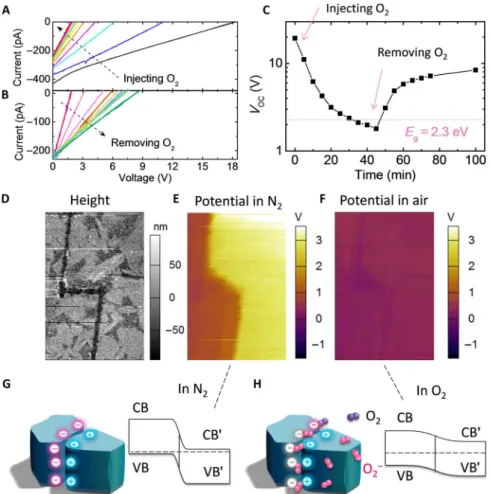
We discovered that the APV effect in OIHP is sensitive to oxygen absorption. For the electrically poled OIHP solar cells with an initial
VOCof 18 V (electrode spacing was 100mm), the APV effect disap-peared gradually when the device was exposed to oxygen (Fig. 4A). This
VOCloss should not relate to material degradation by oxidation because it is reversible. Once the oxygen atmosphere was removed by vacuum-ing, theVOCrecovered to be over-bandgap again (Fig. 4B). At an oxygen pressure of 100 to 1000 Pa, it took about 30 to 40 min for the OIHP solar cells to lose most of theirVOC, and likewise, under a vacuum condition, it took about 30 to 40 min to recover the anomalously largeVOC(Fig. 4C), indicating a quick diffusion of oxygen in and out of the OIHP polycrys-talline films. Under KPFM, the over-bandgap potential difference shown in Fig. 3B disappeared immediately when the atmosphere was changed from N2to air, leaving a residualVOCof ~1.0 V spanning the entire MAPbBr3film (fig. S10). Consistently, the tunneling junctions in MAPbBr3solar cells with controlled ion accumulation disappeared when the sample was exposed to air (Fig. 3, D and F). The disappearance of the tunneling junction may be caused by a much lower doping concentration at GBs by the charge trapping effect of absorbed oxygen (see the scheme in Fig. 4H). Zoharet al.(49) studied the electrochemical reaction in MAPbI3films with impedance spectroscopy, in which the n-type MAPbI3
Fig. 4. Oxygen-sensitive APV effect.(A) Vanished APV due to oxygen injection, where the electrode spacing of OIHP solar cells was 100mm. (B) Recovered APV in the same MAPbBr3device as shown in (A) by pumping oxygen away. (C) Evolution of the photovoltaic against time, where the MAPbBr3solar cells were exposed to oxygen (100 to 1000 Pa)
during the first 45 min and then kept in vacuum from the 46th minute. (D) Topography of the E-beam–patterned MAPbBr3film, where the measured area was 60mm × 90mm.
(E) and (F) show the surface potential images of the electrically poled MAPbBr3film in N2and air, respectively, where the abrupt potential change vanished because of oxygen
absorption. (G) and (H) show the schematic energy diagrams at GBs in N2and air, respectively, where the ion accumulation–induced tunneling junction vanished because of
film was shown to be dedoped toward the intrinsic state when the film was kept in O2-rich ambient. This explains the disappearance of tunneling junction in our study well. This oxygen-sensitive APV effect in OIHP might explain why it was not noticed previously in some other studies carried out in air (47).
In summary, we have demonstrated an APV effect for the first time in MAPbBr3, MAPbI3, and CsPbBr3lateral structure solar cells. The largest obtainedVOC(14 to 18 V) was multiple times larger than the materials’bandgap. This APV effect was not related to the“ ferro-electricity”of OIHP materials, as excluded by the polarized light study and elevated temperature study. This APV effect was sensitive to oxygen absorption. The origins of the APV effect have been proven to be the formation of dispersed tunneling junctions and many staggered local PVUs in OIHP film, which provide an experimentally proven mecha-nism for the explanations of APV effects. This discovery also provides a new strategy to form large and continuously adjustable photovoltages without being limited by the materials’bandgap, which may find new applications in self-powered, highly integrated chips (for example, >5 V) or microelectromechanical systems. Moreover, this work also suggests that ion migration in OIHP is useful in some situations because it enables the formation of novel optoelectronic devices.
MATERIALS AND METHODS
Perovskite precursor synthesis
Methylammonium iodide (CH3NH3I) was synthesized by the method described by Leeet al.(3). A concentrated aqueous solution of hydroiodic acid [15.0 ml, 57 weight % (wt %) in water; Alfa Aesar] was reacted with methylamine (CH3NH2) (13.5 ml, 40 wt % in aqueous solution; Alfa Aesar) at 0°C for 2 hours with constant stirring under nitrogen atmosphere. Methylammonium iodide was crystallized by removing the solvent using a rotary evaporator. The generated white powder was washed three times with diethyl ether (Alfa Aesar) and then dried in a vacuum overnight.
Film formation and device fabrication
The lateral MAPbBr3and MAPbI3devices were fabricated on pre-cleaned glass substrates. First, 75-nm-thick Au electrodes with varied spacings of 8, 30, 50, or 100mm were thermally deposited using a shad-ow mask. Subsequently, a 300-nm-thick MAPbBr3or MAPbI3film was spin-coated on substrate with a“two-step”interdiffusion method. In particular, for the fabrication of MAPbBr3film, PbBr2(45 wt %) and MABr (4.0 wt %) were dissolved in dimethylformamide and 2-propanol, respectively, to form precursor solutions. The PbBr2hot solution was spun onto glass at 6000 rpm. Then, the hot MABr solution was spin-coated on PbBr2film at 6000 rpm for 35 s. The bilayer films were then annealed at 100°C for 1 hour. Similarly, for MAPbI3film, PbI2(40 wt %) and MAI (4.0 wt %) were first dissolved in dimethylformamide and 2-propanol, respectively, to form precursor solutions. The PbI2hot so-lution was spun onto glass at 6000 rpm. Then, the hot MAI soso-lution was spin-coated on PbI2film at 6000 rpm for 35 s. The bilayer films were then annealed at 100°C for 1 hour. The CsPbBr3films were fabricated by a one-step method. The precursor solution was prepared by dissol-ving 149 mg of CsBr and 257 mg of PbBr2in a mixed solvent of 800ml ofN,N′-dimethylformamide and 200ml of dimethyl sulfoxide. The so-lution was stirred overnight and filtered through a polytetrafluoroethylene filter. Then, the precursor solution was spun onto a glass substrate with gold electrodes at 4000 rpm for 30 s. The samples were drop-casted with 120ml of toluene at the eighth second after the spin-coating started. Af-ter spin-coating, the sample was annealed at 100°C for 30 min.
Film and device characterization
Measurements on lateral solar cells were conducted in a probe station chamber under a vacuum of 10−5Pa, with white light (25 mW/cm2) through a quartz window. The substrate was located on a metal plate with its temperature controlled by a heater and injected liquid N2, which could vary from 80 to 340 K. During the testing, the atmosphere of the probe station chamber was changed by injecting dry oxygen gas from a charging valve. A high voltage supply (Keithley 240A) with a maximum available voltage output of 1200 V was used for the poling process. A semi-conductor analyzer (Keithley 4200) was used for theI-Vcharacterization.
KPFM measurements
Measurements were conducted in a small, closed cell with continuous dry N2flow or in air. Pt/Ir-coated conductive probes were used in the KPFM measurements. The two-pass KPFM mode was used to measure the topographic and surface potential signals from the same sample ar-ea. The first pass was used to acquire the morphology, and the second pass was used to acquire the surface potential with the tip lifted by a fixed distance following the surface profile. The scanning area and tip velocity were 90mm × 90mm (or 2mm × 2mm; 4mm/s) and ~54mm/s, respectively. The tip-surface distance for KPFM measurements was 40 nm for all samples. During testing, the perovskite solar cells were kept under open-circuit conditions with the cathode grounded within the shield of the equipment. A white light with an intensity of ~100 mW/cm2was shined from the bottom of the transparent glass substrate. All the KPFM mea-surements were carried out at least 10 to 15 min after the electrical poling. The KPFM scanning process itself usually lasts for 20 to 200 min (turn light on, turn light off, change locations, adjust the N2flow, etc.). During the KPFM scanning, the solar cells were kept under open-circuit conditions with no bias applied.
SUPPLEMENTARY MATERIALS
Supplementary material for this article is available at http://advances.sciencemag.org/cgi/ content/full/3/3/e1602164/DC1
fig. S1. APV effect in lateral MAPbI3solar cells.
fig. S2. Independence of the APV effect on light polarization directions.
fig. S3. APV effect in nonpolar CsPbBr3-based lateral perovskite solar cells.
fig. S4.I-Vcurves of electrically poled MAPbBr3lateral solar cells at different temperatures.
fig. S5. Stabilities of the APV effect under dark and illuminating conditions.
fig. S6. Accelerated degradation of MAPbBr3polycrystalline films by illumination and
vacuuming.
fig. S7. Continuously formed over-bandgapVOCin MAPbBr3solar cells.
fig. S8. Illustration of the GB broadening process caused by E-beam treatment.
fig. S9. Illustration of the proposed working mechanism for dispersed tunneling junction–
induced APV effect.
fig. S10. Disappearance of APV effect induced by oxygen absorption.
table S1.VOCobtained at forward and backward scanning at different temperatures.
REFERENCES AND NOTES
1. J. Burschka, N. Pellet, S.-J. Moon, R. Humphry-Baker, P. Gao, M. K. Nazeeruddin, M. Grätzel, Sequential deposition as a route to high-performance perovskite-sensitized solar cells.
Nature499, 316–319 (2013).
2. M. Liu, M. B. Johnston, H. J. Snaith, Efficient planar heterojunction perovskite solar cells by
vapour deposition.Nature501, 395–398 (2013).
3. M. M. Lee, J. Teuscher, T. Miyasaka, T. N. Murakami, H. J. Snaith, Efficient hybrid solar
cells based on meso-superstructured organometal halide perovskites.Science338,
643–647 (2012).
4. G. Hodes, Perovskite-based solar cells.Science342, 317–318 (2013).
5. N.-G. Park, Organometal perovskite light absorbers toward a 20% efficiency low-cost
solid-state mesoscopic solar cell.J. Phys. Chem. Lett.4, 2423–2429 (2013).
6. J. H. Heo, S. H. Im, J. H. Noh, T. N. Mandal, C.-S. Lim, J. A. Chang, Y. H. Lee, H.-j. Kim,
hybrid heterojunction solar cells containing perovskite compound and polymeric hole
conductors.Nat. Photonics7, 486–491 (2013).
7. H. Zhou, Q. Chen, G. Li, S. Luo, T.-b. Song, H.-S. Duan, Z. Hong, J. You, Y. Liu, Y. Yang,
Interface engineering of highly efficient perovskite solar cells.Science345,
542–546 (2014).
8. W. S. Yang, J. H. Noh, N. J. Jeon, Y. C. Kim, S. Ryu, J. Seo, S. I. Seok, High-performance
photovoltaic perovskite layers fabricated through intramolecular exchange.Science348,
1234–1237 (2015).
9. N. J. Jeon, J. H. Noh, W. S. Yang, Y. C. Kim, S. Ryu, J. Seo, S. I. Seok, Compositional
engineering of perovskite materials for high-performance solar cells.Nature517,
476–480 (2015).
10. Y. Shao, Y. Yuan, J. Huang, Correlation of energy disorder and open-circuit voltage in
hybrid perovskite solar cells.Nat. Energy1, 15001 (2016).
11. G. Xing, N. Mathews, S. S. Lim, N. Yantara, X. Liu, D. Sabba, M. Grätzel, S. Mhaisalkar, T. C. Sum, Low-temperature solution-processed wavelength-tunable perovskites
for lasing.Nat. Mater.13, 476–480 (2014).
12. H. Zhu, Y. Fu, F. Meng, X. Wu, Z. Gong, Q. Ding, M. V. Gustafsson, M. T. Trinh, S. Jin, X.-Y. Zhu, Lead halide perovskite nanowire lasers with low lasing thresholds and high
quality factors.Nat. Mater.14, 636–642 (2015).
13. R. Dong, Y. Fang, J. Chae, J. Dai, Z. Xiao, Q. Dong, Y. Yuan, A. Centrone, X. C. Zeng, J. Huang, High-gain and low-driving-voltage photodetectors based on organolead
triiodide perovskites.Adv. Mater.27, 1912–1918 (2015).
14. H. Wei, Y. Fang, P. Mulligan, W. Chuirazzi, H.-H. Fang, C. Wang, B. R. Ecker, Y. Gao, M. A. Loi, L. Cao, J. Huang, Sensitive X-ray detectors made of methylammonium lead
tribromide perovskite single crystals.Nat. Photonics10, 333–339 (2016).
15. Z.-K. Tan, R. S. Moghaddam, M. L. Lai, P. Docampo, R. Higler, F. Deschler, M. Price, A. Sadhanala, L. M. Pazos, D. Credgington, F. Hanusch, T. Bein, H. J. Snaith, R. H. Friend,
Bright light-emitting diodes based on organometal halide perovskite.Nat.
Nanotechnol.9, 687–692 (2014).
16. X. Y. Chin, D. Cortecchia, J. Yin, A. Bruno, C. Soci, Lead iodide perovskite light-emitting
field-effect transistor.Nat. Commun.6, 7383 (2015).
17. Z. Xiao, Y. Yuan, Y. Shao, Q. Wang, Q. Dong, C. Bi, P. Sharma, A. Gruverman, J. Huang, Giant switchable photovoltaic effect in organometal trihalide perovskite devices.
Nat. Mater.14, 193–198 (2015).
18. C. Eames, J. M. Frost, P. R. F. Barnes, B. C. O’Regan, A. Walsh, M. S. Islam, Ionic transport in
hybrid lead iodide perovskite solar cells.Nat. Commun.6, 7497 (2015).
19. Y. Yuan, J. Chae, Y. Shao, Q. Wang, Z. Xiao, A. Centrone, J. Huang, Photovoltaic switching
mechanism in lateral structure hybrid perovskite solar cells.Adv. Energy Mater.5,
1500615 (2015).
20. T. M. Brenner, D. A. Egger, L. Kronik, G. Hodes, D. Cahen, Hybrid organic–inorganic
perovskites: Low-cost semiconductors with intriguing charge-transport properties.Nat.
Rev. Mater.1, 15007 (2016).
21. Y. Yuan, Q. Wang, Y. Shao, H. Lu, T. Li, A. Gruverman, J. Huang, Electric-field-driven reversible conversion between methylammonium lead triiodide perovskites and lead
iodide at elevated temperatures.Adv. Energy Mater.6, 1501803 (2015).
22. Z. Xiao, J. Huang, Energy-efficient hybrid perovskite memristors and synaptic devices.
Adv. Electron. Mater.2, 1600100 (2016).
23. G. Xing, N. Mathews, S. Sun, S. S. Lim, Y. M. Lam, M. Grätzel, S. Mhaisalkar, T. C. Sum, Long-range balanced electron- and hole-transport lengths in organic-inorganic CH3NH3PbI3.Science342, 344–347 (2013).
24. S. D. Stranks, G. E. Eperon, G. Grancini, C. Menelaou, M. J. P. Alcocer, T. Leijtens, L. M. Herz, A. Petrozza, H. J. Snaith, Electron-hole diffusion lengths exceeding 1 micrometer in an
organometal trihalide perovskite absorber.Science342, 341–344 (2013).
25. Y. Yuan, Z. Xiao, B. Yang, J. Huang, Arising applications of ferroelectric materials in
photovoltaic devices.J. Mater. Chem.2, 6027–6041 (2014).
26. S. Yang, S. J. Byrnes, P. Shafer, C.-H. Yang, M. D. Rossell, P. Yu, Y.-H. Chu, J. F. Scott, J. W. Ager III, L. W. Martin, R. Ramesh, Above-bandgap voltages from ferroelectric
photovoltaic devices.Nat. Nanotechnol.5, 143–147 (2010).
27. T. Choi, S. Lee, Y. J. Choi, V. Kiryukhin, S.-W. Cheong, Switchable ferroelectric diode and
photovoltaic effect in BiFeo3.Science324, 63–66 (2009).
28. R. Guo, L. You, Y. Zhou, Z. S. Lim, X. Zou, L. Chen, R. Ramesh, J. Wang, Non-volatile
memory based on the ferroelectric photovoltaic effect.Nat. Commun.4, 1990 (2013).
29. F. Zheng, H. Takenaka, F. Wang, N. Z. Koocher, A. M. Rappe, First-principles calculation of
the bulk photovoltaic effect in CH3NH3PbI3and CH3NH3PbI3–xClx.J. Phys. Chem. Lett.
6, 31–37 (2014).
30. V. M. Fridkin, Bulk photovoltaic effect in noncentrosymmetric crystals.Crystallogr. Rep.46,
654–658 (2001).
31. J. Starkiewicz, L. Sosnowski, O. Simpson, Photovoltaic effects exhibited in high-resistance
semi-conducting films.Nature158, 28 (1946).
32. S. Ryu, J. H. Noh, N. J. Jeon, Y. C. Kim, W. S. Yang, J. Seo, S. I. Seok, Voltage output of
efficient perovskite solar cells with high open-circuit voltage and fill factor.Energy
Environ. Sci.7, 2614–2618 (2014).
33. R. Sheng, A. Ho-Baillie, S. Huang, S. Chen, X. Wen, X. Hao, M. A. Green, Methylammonium
lead bromide perovskite-based solar cells by vapor-assisted deposition.J. Phys.
Chem. C119, 3545–3549 (2015).
34. A. M. Glass, D. Von der Linde, T. J. Negran, High-voltage bulk photovoltaic effect and the
photorefractive process in LiNbO3.Appl. Phys. Lett.25, 233–235 (1974).
35. S. Liu, F. Zheng, N. Z. Koocher, H. Takenaka, F. Wang, A. M. Rappe, Ferroelectric domain wall induced band gap reduction and charge separation in organometal halide
perovskites.J. Phys. Chem. Lett.6, 693–699 (2015).
36. D. A. Egger, A. M. Rappe, L. Kronik, Hybrid organic–inorganic perovskites on the move.
Acc. Chem. Res.49, 573–581 (2016).
37. A. A. Bakulin, O. Selig, H. J. Bakker, Y. L. A. Rezus, C. Müller, T. Glaser, R. Lovrincic, Z. Sun, Z. Chen, A. Walsh, J. M. Frost, T. L. C. Jansen, Real-time observation of organic cation
reorientation in methylammonium lead iodide perovskites.J. Phys. Chem. Lett.6,
3663–3669 (2015).
38. A. M. A. Leguy, J. M. Frost, A. P. McMahon, V. G. Sakai, W. Kockelmann, C. Law, X. Li,
F. Foglia, A. Walsh, B. C. O’Regan, J. Nelson, J. T. Cabral, P. R. F. Barnes, The dynamics of
methylammonium ions in hybrid organic–inorganic perovskite solar cells.Nat.
Commun.6, 7124 (2015).
39. J. M. Frost, A. Walsh, What is moving in hybrid halide perovskite solar cells?Acc. Chem.
Res.49, 528–535 (2016).
40. E. Mosconi, C. Quarti, T. Ivanovska, G. Ruani, F. De Angelis, Structural and electronic
properties of organo-halide lead perovskites: A combined IR-spectroscopy andab initio
molecular dynamics investigation.Phys. Chem. Chem. Phys.16, 16137–16144 (2014).
41. H. Zhu, K. Miyata, Y. Fu, J. Wang, P. P. Joshi, D. Niesner, K. W. Williams, S. Jin, X.-Y. Zhu, Screening in crystalline liquids protects energetic carriers in hybrid perovskites.
Science353, 1409–1413 (2016).
42. Y. Kutes, L. Ye, Y. Zhou, S. Pang, B. D. Huey, N. P. Padture, Direct observation of
ferroelectric domains in solution-processed CH3NH3PbI3perovskite thin films.J. Phys.
Chem. Lett.5, 3335–3339 (2014).
43. M. Coll, A. Gomez, E. Mas-Marza, O. Almora, G. Garcia-Belmonte, M. Campoy-Quiles, J. Bisquert, Polarization switching and light-enhanced piezoelectricity in lead
halide perovskites.J. Phys. Chem. Lett.6, 1408–1413 (2015).
44. S. Liu, F. Zheng, I. Grinberg, A. M. Rappe, Photoferroelectric and photopiezoelectric
properties of organometal halide perovskites.J. Phys. Chem. Lett.7, 1460–1465 (2016).
45. E. T. Hoke, D. J. Slotcavage, E. R. Dohner, A. R. Bowring, H. I. Karunadasa, M. D. McGehee, Reversible photo-induced trap formation in mixed-halide hybrid
perovskites for photovoltaics.Chem. Sci.6, 613–617 (2015).
46. Y. Shao, Y. Fang, T. Li, Q. Wang, Q. Dong, Y. Deng, Y. Yuan, H. Wei, M. Wang, A. Gruverman, J. Shielda, J. Huanga, Grain boundary dominated ion migration in polycrystalline
organic–inorganic halide perovskite films.Energy Environ. Sci.9, 1752–1759 (2016).
47. Y. Yuan, J. Huang, Ion migration in organometal trihalide perovskite and its impact on
photovoltaic efficiency and stability.Acc. Chem. Res.49, 286–293 (2016).
48. E. J. Juarez-Perez, R. S. Sanchez, L. Badia, G. Garcia-Belmonte, Y. S. Kang, I. Mora-Sero, J. Bisquert, Photoinduced giant dielectric constant in lead halide perovskite solar
cells.J. Phys. Chem. Lett.5, 2390–2394 (2014).
49. A. Zohar, N. Kedem, I. Levine, D. Zohar, A. Vilan, D. Ehre, G. Hodes, D. Cahen, Impedance
spectroscopic indication for solid state electrochemical reaction in (CH3NH3)PbI3
films.J. Phys. Chem. Lett.7, 191–197 (2015).
Acknowledgments
Funding:We thank the financial support from NSF (ECCS-1252623 and DMR-1505535). Author contributions:J.H. and Y.Y. designed the experiments, analyzed the data, and wrote the paper. Y.Y. carried out most of the device fabrication and characterization. T.L. carried out the KPFM measurements, and Y.Y. was involved with sample treatment. A.G. analyzed the KPFM data.
Q.W. prepared the perovskite samples. J.X. studied CsPbBr3devices. Q.W. carried out SEM and
energy-dispersive x-ray measurement. The following authors were responsible for providing the figures included in this study: Fig. 1, Y.Y.; Fig. 2, Y.Y.; Fig. 3, T.L. and Y.Y.; Fig. 4 (A to C), Y.Y.; Fig. 4 (D to H), T.L. and Y.Y.; fig. S1, Y.Y.; fig. S2, J.X. and Q.W.; fig. S3, J.X. and Q.W.; fig. S4, Y.Y.; fig. S5, Y.Y.; fig. S6, Y.Y.; fig. S7, T.L. and Y.Y.; fig. S8, Y.Y.; fig. S9, Y.Y.; and fig. S10, T.L. and Y.Y. All the authors
commented on the paper.Competing interests:The authors declare that they have no
competing interests.Data and materials availability:All data needed to evaluate the conclusions
in the paper are present in the paper and/or the Supplementary Materials. Additional data related to this paper may be requested from the authors.
Submitted 8 September 2016 Accepted 3 February 2017 Published 17 March 2017 10.1126/sciadv.1602164
Citation:Y. Yuan, T. Li, Q. Wang, J. Xing, A. Gruverman, J. Huang, Anomalous photovoltaic