FPGA IMPLEMENTATION OF RC4 STREAM CIPHER
CRYPTOGRAPHY ALGORITHM
S. Kishore Reddy*A. Ravi Shankar**
ABSTRACT
In this paper, an efficient hardware implementation of the RC4 stream-cipher is proposed. In
contrary to previous designs, which support only fixed length key, the proposed
implementation integrates in the same hardware module an 8-bit up to 128-bit key length
capability. Independently of the key length, the proposed VLSI implementation achieves a
data throughput up to 22 MBytes/sec in a maximum frequency of64 MHz The whole design
was captured by using VHDL language and a FPGA device was used for the hardware
implementation of the architecture. A detailed analysis, in terms of performance, and covered
area is shown.
*Associate Professor, Department of ECE, SITS, Khammam.
I. INTRODUCTION
The main feature of cryptography is to work out with problems, which are associated with
secrecy, authentication and integrity. Cryptography also, is related with the meaning of
protocol. A protocol is sequences of actions, which are concern two or more sides, designed
to fulfill a goal. Thus, a cryptographic protocol is a protocol that uses cryptography. This
protocol uses a cryptographic algorithm and its intention is to prevent attempts of thefts and
invasions. Nowadays cryptography has been developed in a science strongly validated using
terms of Theory of Statistics and Theory of Numbers [1, 2].
In order to handle all the cryptographic problems many kinds of cryptographic algorithms
have been invented. The complexity of these problems made several categories of
cryptographic algorithms. A much known is the RC4 stream cipher.
RC4 is a variable-key-size stream cipher developed in 1987 by Ron Rivest for RSA Data
Security, Inc. While some key weakness have been introduced [3], the RC4 is used for
encryption in the wired equivalent privacy (WEP) [4] protocol (part of the IEEE 802.1 lb
wireless LAN security standard), IEEE 802.11 i [5], Lotus Notes, Apple computer's AOCE
and Oracle secure SQL. The IEEE 802.11 i uses the Temporal Key Integrity Protocol (TKIP)
and the Advanced Encryption Standard (AES) [6]. TKIP uses the RC4 stream cipher as the
encryption and decryption algorithm and all involved parties must share the same secret key.
The RC4 stream cipher works in two phases, key setup and ciphering. During an n-bit key
setup (n is the key length), the encryption key is used to generate an encrypting variable using
two arrays, state and key, and n number of mixing operations [I].
In this paper a new hardware implementation of the RC4 stream cipher. is presented. The
implementation is parameterized in order to support variable key lengths. The key length
could be 8-bit up to 128-bit opposed to the previous designs [7, 8, 9] that supports only fixed
key lengths. The proposed implementation needs three clock cycles per byte generation, in
the key setup phase, and three clock cycles per byte generation, in the ciphering phase. 768 +
3*n clock cycles needs at total, (n is the number of bytes of the plaintext/cipher text), to
complete the whole operation. Comparing with the implementations in [7, 8] the proposed
one is much faster. The implementation in [9] needs the same time (768 + 3*n clock cycles)
with the proposed one but works with fixed key 40-bit in length. Finally, in [101 a RC4
stream cipher software implementation is presented. In this implementation assembly
main disadvantage of this implementation is that encrypts/decrypts one byte at every
seven-clock cycles resulting a rapid increment of the algorithmic latency.
The paper is organized as follows. Section 11 describes the RC4 stream cipher. In section III
the proposed architecture is presented and analyzed in details. The VLSI implementation
results are shown and discussed in section IV and finally conclusions are given in section V
II. RC4 STREAM CIPHER
RC4 uses a variable length key from I to 256 bytes to initialize a 256-byte array. The array is
used for subsequent generation of pseudo-random bytes and then generates a pseudorandom
stream, which is XORed with the plaintext/cipher text to give the cipher text/plaintext.
It works in Output Feedback (OFB) mode [II] of operation. There are two 256-byte arrays,
S-Box and K-S-Box. The S-array is filled linearly, such as S0=0, Sl=l, S2=2, .... S255=255. The
K-array consists of the key, repeating as necessary times, in order to fill the array. The RC4
stream cipher works in two phases. The key setup phase and the pseudorandom key stream
generator phase. Both phases must be performed for every new key.
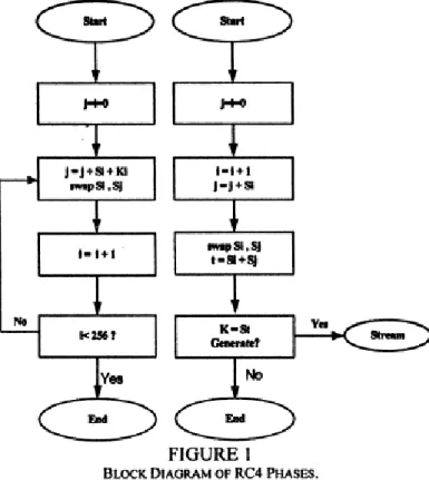
Figure 1 shows the block diagram of the RC4 two phases
.
RC4 uses two counters, i and j, which are initialized to zero. In the key setup phase the S-box
Key setup phase:
fori= Oto 255
j = (j + Si + K1) mod 256
swap Si and Sj
Once the key setup phase is completed the second phase encrypts or decrypts a message. The
pseudorandom number generator (PRGN) phase is described by the following pseudo code:
Key stream generation phase:
i=(i+ 1)mod256
j = (j + S) mod 256
swap S, and Sj
t = (Si + Sj) mod 256
K = Si
The key stream K is XORed with the plaintext/cipher text to produce cipher text/plaintext.
III. PROPOSED ARCHITECTURE
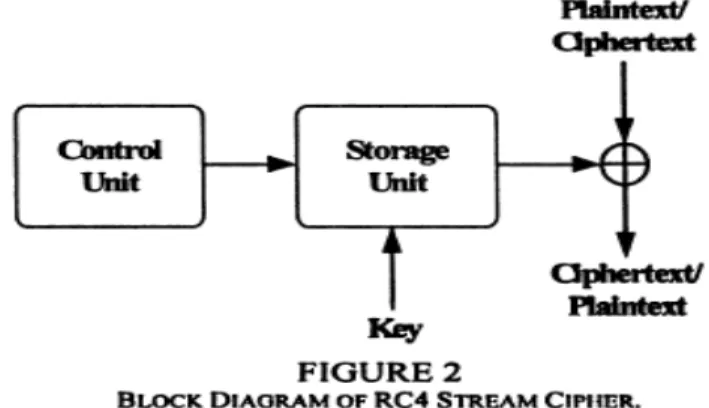
Figure 2 shows the block diagram of the proposed architecture. It consists of a control and a
storage unit. The storage unit is responsible for the key setup and key stream generation.
The implementation of the storage unit is shown in Fig. 3. The storage unit contains memory
elements for the S Box and K-Box, along with 8-bit registers, adders and one multiplexer.
The block diagram of the S-box RAM is shown Fig. 4. It consists of three 256 bytes RAM
blocks. Each RAM block has four inputs and one output. The two inputs are the read and
write signals while the other two are the address and data signals. Also, all the three RAM
boxes have the same signals of clock and reset. The operation of RAM blocks is quite simple.
If the reset signal occurs the blocks are initialized linearly. For each block, if the write signal
occurs new data are stored in the address position, or if the read signal occurs the data in the
The two first blocks i, j (Fig. 4) are used for the swapping of the values of the third block t.
The final values that are used for the algorithm are produced by the t block.
First, the key setup phase is divided in two steps. In the first step the box is filled. The
S-Box is initialized linearly, such as So=O, Sl=l, S2=2…S255=255 when the reset state occurs.
In the second step of the key setup, the S-Box is randomizely filled. For the S-box,
3x256-bytes RAM memory is used as it's shown in Fig. 4. The Si and Sj registers are used for the
necessary by the algorithm swappings. The j_ ant t_ registers are used in order to temporary
At the first clock cycle the value of counter i (see Fig. 3) is used as address in the first RAM
block. The value of Si is used for the computation of the new value ofj as it is shown in Fig.
3. It is stored in the Si-register. The two adders are used for the computation of the new value
ofj. They accept as input the values of Ki and Si. At the second clock cycle the new produced
value j is used as address for the second RAM block. The stored value in this address is
temporary stored in the Sj_register. At the third cycle the contents of the Si_register and Sj
register are written at the j and i addresses correspondingly. With this procedure, the
swapping is achieved.
This step needs three clock cycles per iteration. So, the total cycles that are needed in the key
setup phase are 256 *3= 768.
The second phase is quite similar with the first phase and so; the same hardware is being
used. The difference in this phase is that the values of the K-Box are not used. After, the first
zero -so as to be ready for the second phase. After the two mentioned phases, the procedure
of stream generation can begin.
The operations at the first three steps are similar to those of the key setup phase except that
the S-Box is already initialized. At the first step the value of i is used as address in the first
RAM block, the value of Si is stored in the Si_register. Also the new value of j is computed.
At the second step the new value of j is used as address of the second RAM block and the
value of Sj is stored in the Sj]register. In this step the values of Si and Sj are being added and
the result of the addition is stored in the St_register. At the third step the contents of the Si
register and Sj register are written at the j and i addresses correspondingly and the value of
the t_register is being used as address for the third RAM block. So, the value of St is also
produced in the third step. This value of St is the stream-generated byte.
After the completion of this phase, each byte in the key stream can be generated and used for
encryption/decryption. The encryption/decryption is achieved by the bitwise XORing of the
key stream with the plaintext/cipher text.
The t6tal duration time of this phase is 3*n (n is the number of bytes of the plaintext or cipher
text) and the total duration time of the whole procedure of the two phases is 768 + 3*n.
The operation of the storage unit is synchronized by the control unit. The control unit is
responsible for the generation of the clock and control signals.
IV. VLSI IMPLEMENTATION RESULTS
The proposed architecture was captured by using VHDL. All the system components were
described with structural architecture. The system tested using confirmed test vectors [12] in
order to examine its correctness. The whole design was synthesized, placed and routed by
using XILINX FPGA device [13]. Synthesis results for the proposed implementation are
The VIRTEX XILINX 2V250FG256 device has 18K bit select RAM blocks. Each block is
synchronous and can be easily configured in 256-byte RAM block. The proposed
implementation uses a 3*256-byte RAM blocks.
Comparison between the proposed RC4 implementation and other previous reported
Implementations [7, 10] are presented in Table II..
The implementation results are referred for the same FPGA module. The rest of the previous
publications did not give information about the performance.
For the full execution of the algorithm the proposed implementation needs 768 + 3*n clock
cycles (n is the number of bytes of the plaintext/cipher text). The implementation in [8] needs
1280 + 4*n clock cycles. 256 cycles in order to fill linearly the S-Box, and 1024 cycles for
the key setup phase.
The implementation in [9] needs the same time (768 + 3*n clock cycles) with the proposed
one but works only with fixed key 40-bit in length. Finally, the software implementation in
[101 encrypts/decrypts one byte at every seven clock cycles and of course increases the total
latency of the algorithm execution.
V. CONCLUSIONS
A VLSI implementation of the RC4 stream cipher is presented in this paper. The proposed
design provides high data throughput using 8-bit word and variable key length, from 8-bit to
128-bit, contrary to previous designs, which support only fixed length key. It provides
flexibility as it can be used in many applications with any key length from 8-bit to 128-bit.
The proposed system achieves a data throughput up to 22 MBytes/sec in a clock frequency of
64 MHz. The measurement results and comparisons with previous implementations prove
that the proposed one is a flexible solution for any cryptographic system.
VI. REFERENCES
[1] B. Schneier, "Applied Cryptography - Protocols, Algorithms and Source Code in C",
[2] A. Menezes, P. van Oorschot, and S. Vanstone, "Handbook ofApplied Cryptography",
CRC Press, 1996.
[3] S. Fluhrer, I. Mantin, and A. Shamir. "Weaknesses in the key scheduling algorithm of
RC4 ". In Proc. 8ih Workshop on Selected Areas in Cryptography, LNCS 2259. Springer
Verlag, 2001.
[4] Overview of IEEE 802.1 lb Security, Intel Technology Journal Q2, 2000.
[5] 802.1 1 i Overview Part I, Jesse Walker, Intel Corporation,
http;//wwvw.ocate.edu/wirelcss 4.ppt
[6] "Advanced encryption standard"
[7] P. Hamalainen, M. Hannikainen, T. Hamalainen and J. Snarinen, "Hardware
Implementation of the Improved WEP and RC4 Encryption Algorithms for Wireless
Terminals", The European Signal Processing Conference (EUSIPCO'2000), September 5-8,
2000, Tampere, Finland, pp. 2289-2292.
[8] P. D. Kundarewicl', S. J.E. Wilton, A. J. Hu,"'A CPLD- Based RC4 Cracking
System",,The 1999 Canadian Conference on Electrical and Computer Engineering, May
1999.
[9] K.H Tsoi, K.H Lee and P.H.W Leong, "A Massively Parallel RC4 Key Search Engine",
Proc. of the IOth Annual IEEE Symposium on Field-Programmable Custom Computing
Machines (FCCM'02), September 22 - 24, 2002 Napa, California, pp. 13-21.
[10] B. Schneier, D. Whiting, "Fast Software Encryption: Designing Encryption Algorithms
for Optimal Software Speed on the Intel Pentium Processor", Fast Software Encryption
workshop (FSE97), LNCS, Vol. 1267, pp. 242-259, Springer-Verlag, Haifa, Israel, January
20-22, 1997.
[11] "Recommendation for Block Cipher Modes of Operation. Methods and Techniques".
National Institute of Standards and Technology, Technology Administration, U.S.
Department of Commerc
[12] Confirmed Test Vector for RC
[13] Xilinx Inc., San Jose, Calif., "Virtex, 2.5 V Field Programmable Gate Arrays," 2003,