Agilent
Vector Signal Analysis Basics
This application note serves as a primer on the vector signal analyzer (VSA). This chapter discusses VSA measurement concepts and theory of operation; Chapter 2 discusses VSA vector-modulation analysis and, specifically, digital-modulation analysis.
Analog, swept-tuned spectrum analyzers use superheterodyne technology to cover wide frequency ranges; from audio, through microwave, to millimeter frequencies. Fast Fourier transform (FFT) analyzers use digital signal
processing (DSP) to provide high-resolution spectrum and network analysis, but are limited to low frequencies due to the limits of analog-to-digital conversion (ADC) and signal processing technologies. Today’s wide-bandwidth, vector-modulated (also called complex or digitally modulated), time-varying signals benefit greatly from the capabilities of FFT analysis and other DSP techniques. VSAs combine superheterodyne technology with high speed ADCs and other DSP technologies to offer fast, high-resolution spectrum measurements, demodulation, and advanced time-domain analysis. A VSA is especially useful for characterizing complex signals such as burst, transient, or modulated signals used in communications, video, broadcast, sonar, and ultrasound imaging applications.
Figure 1-1 shows a simplified block diagram of a VSA analyzer. The VSA implements a very different measurement approach than traditional swept analyzers; the analog IF section is replaced by a digital IF section incorporating FFT technology and digital signal processing. The traditional swept-tuned spectrum analyzer is an analog system; the VSA is fundamentally a digital system that uses digital data and mathematical algorithms to perform data analysis. For example, most traditional hardware functions, such as mixing, filtering, and demodulation, are accomplished digitally, as are many measurement operations. The FFT algorithm is used for spectrum analysis, and the demodulator algorithms are used for vector analysis applications.
Chapter 1
Vector Signal Analyzer
ADC Time Anti-alias filter Quadrature detector, digital filtering FFT IF input Local oscilator RF input Time domain Frequency domain Modulation domain Code domain t f I Q 0 code 15 I Q Demod-ulator 90 degs t t
Analog data Digitized data stream
Digital IF and DSP techniques
LO
Figure 1-1. The vector signal analyzer digitizes the analog input signal and uses DSP technology to process and provide data outputs; the FFT algorithm produces frequency domain results, the demodulator algorithms produce modulation and code domain results
A significant characteristic of the VSA is that it is designed to measure and manipulate complex data. In fact, it is called a vector signal analyzer because it has the ability to vector detect an input signal (measure the magnitude and phase of the input signal). You will learn about vector modulation and detection in Chapter 2. It is basically a measurement receiver with system architecture that is analogous to, but not identical to, a digital communications receiver. Though similar to an FFT analyzer, VSAs cover RF and microwave ranges, plus additional modulation-domain analysis capability. These advancements are made possible through digital technologies such as analog-to-digital conversion and DSP that include digital intermediate frequency (IF) techniques and fast Fourier transform (FFT) analysis. Because the signals that people must analyze are growing more complex, the latest generations of spectrum analyzers have moved to a digital architecture and often include many of the vector signal analysis capabilities previously found only in VSAs. Some analyzers digitize the signal at the instrument input, after some amplification, or after one or more downconverter stages. In any of these cases, phase as well as magnitude is preserved in order to perform true vector measurements. Capabilities are then determined by the digital signal processing capability inherent in the spectrum analyzer firmware or available as add-on software running either internally
(measurement personalities) or externally (vector signal analysis software) on a computer connected to the analyzer.
VSA measurement advantages
Vector analysis measures dynamic signals and produces complex data results
The VSA offers some distinct advantages over analog swept-tuned analysis. One of the major advantages of the VSA is its ability to better measure dynamic signals. Dynamic signals generally fall into one of two categories: time-varying or complex modulated. Time-varying are signals whose measured properties change during a measurement sweep (such as burst, gated, pulsed, or transient). Complex-modulated signals cannot be solely described in terms of simple AM, FM, or PM modulation, and include most of those used in digital communications, such as quadrature amplitude modulation (QAM).t
0
Display shows full spectral display A
f f1 f2
Simulated parallel-filter processing Time domain
Vector analysis
Fourier analysis Frequency domain
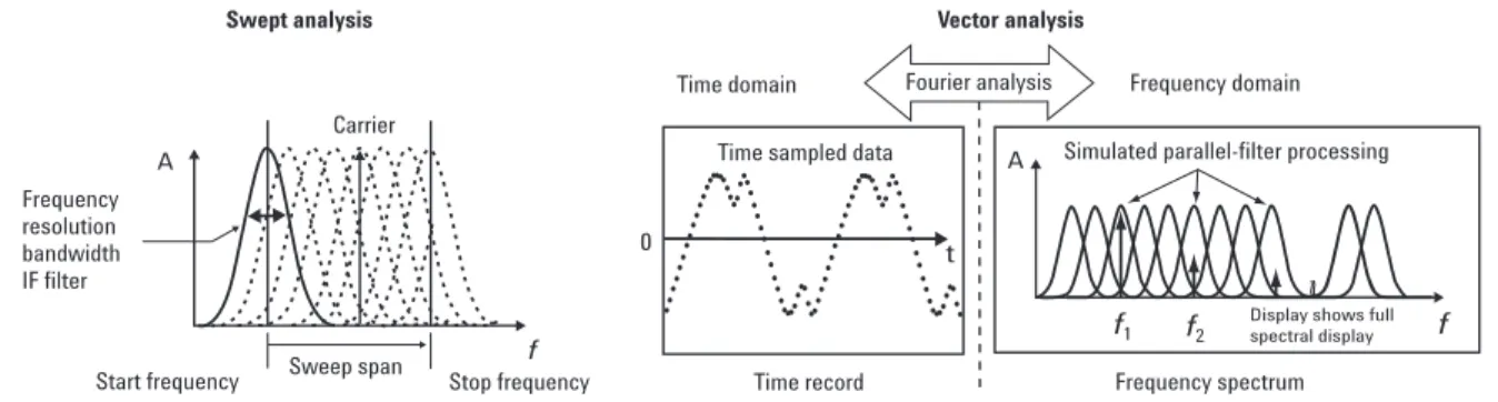
Time record Frequency resolution bandwidth IF filter Swept analysis Carrier Sweep span
Start frequency Stop frequency
f
Time sampled data A
Frequency spectrum
Figure 1-2. Swept-tuned analysis displays the instantaneous time response of a narrowband IF filter to the input signal. Vector analysis uses FFT analysis to transform a set of time domain samples into frequency domain spectra.
1. For more information on spectrum analyzers, see Agilent Application Note 150, Spectrum Analysis Basics, literature number 5952-0292.
A traditional swept-spectrum analyzer1, in effect, sweeps a narrowband
filter across a range of frequencies, sequentially measuring one frequency at a time. Unfortunately, sweeping the input works well for stable or repetitive signals, but will not accurately represent signals that change during the sweep. Also, this technique only provides scalar (magnitude only) information, though some other signal characteristics can be derived by further analysis of spectrum measurements.
The VSA measurement process simulates a parallel bank of filters and overcomes swept limitations by taking a “snapshot,” or time-record, of the signal; then processing all frequencies simultaneously. For example, if the input is a transient signal, the entire signal event is captured (meaning all aspects of the signal at that moment in time are digitized and captured); then used by the FFT to compute the “instantaneous” complex spectra versus frequency. This process can be performed in real-time, that is, without missing any part of the input signal. For these reasons, the VSA is sometimes referred to as a “dynamic signal analyzer” or a “real-time signal analyzer”. The VSA’s ability to track a fast-changing signal isn’t unlimited, however; it depends on the VSA’s computational capability.
The VSA decreases measurement time
Parallel processing yields another potential advantage for high-resolution (narrow resolution bandwidth) measurements; faster measurement time. If you’ve used a swept-tuned spectrum analyzer before, you already know that narrow resolution bandwidth (RBW) measurements of small frequency spans can be very time-consuming. Swept-tuned analyzers sweep frequencies from point to point slowly enough to allow the analog resolution bandwidth filters to settle. By contrast, the VSA measures across the entire frequency span at one time. However, there is analogous VSA settling time due to the digital filters and DSP. This means the VSA sweep speed is limited by data collection and digital processing time rather than analog filters. But this time is usually negligible when compared to the settling time of analog filters. For certain narrow bandwidth measurements, the VSA can complete a measurement up to 1000 times faster than conventional swept-tuned analyzers.
In a swept-tuned spectrum analyzer, the physical bandwidth of the sweeping filter limits the frequency resolution. The VSA doesn’t have this limitation. Some VSAs can resolve signals that are spaced less than 100 µHz apart. Typically, VSA resolution is limited by source and analyzer frequency stability, as well as by the amount of time you are willing to devote to the measurement. Increasing the resolution also increases the time it takes to measure the signal (the length of the required time-record).
Time-capture is a great tool for signal analysis and troubleshooting
Another feature that is extremely useful is the time-capture capability. This allows you to record actual signals in their entirety without gaps, and replay them later for any type of data analysis. The full set of measurement features can be applied to the captured signal. For example, you could capture a transmitted digital communications signal and then perform both spectrum and vector-modulation analysis to measure signal quality or identify signal impairments.DSP provides multi-domain measurements in one instrument
The use of digital signal processing (DSP) also yields additional benefits; it provides time, frequency, modulation, and code domain measurement analysis in one instrument. Having these capabilities increases the analyzer’s value to you and improves the quality of your measurements. FFT analysis allows easy and accurate views of both time and frequency domain data. The DSP provides vector modulation analysis, including both analog and digital modulation analysis. The analog demodulator produces AM, FM and PM demodulation results, similar to that of a modulation analyzer, allowing you to view amplitude, frequency, and phase profiles versus time. The digital demodulator performs a broad range of measurements on many digital communications standards (such as W-CDMA, GSM, cdma2000, and more) and produces many useful measurement displays and signal-quality data.
Although the VSA clearly provides important benefits, the conventional analog swept-tuned analyzers can provide higher frequency coverage and increased dynamic range capability.
VSA measurement concepts and theory of operation
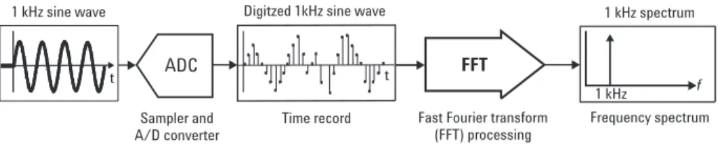
As mentioned earlier, the VSA is fundamentally a digital system that uses DSP to perform spectrum analysis with FFTs, and uses demodulator algorithms to perform vector-modulation analysis. You may recall from Fourier analysis, that the FFT is a mathematical algorithm that operates on time-sampled data and provides time-to-frequency domain transformations. The analog signal must be digitized in the time-domain, then the FFT algorithm executes to compute the spectra. Conceptually, the VSA implementation is simple and straightforward: digitize the input signal, then compute the measurement results. See Figure 1-3. However, in practice, there are many factors that must be accounted for in order for the measurement to be meaningful and accurate. (For more information about FFT analysis, refer to the Referencessection at the end of this application note.) ... .. . ... . ..... .... .. ... .. .. .. .. . .. . ...... . . ADC FFT Time record Sampler and A/D converter Frequency spectrum 1 kHz sine wave Digitzed 1kHz sine wave1 kHz f
Fast Fourier transform (FFT) processing t
1 kHz spectrum
t
Figure 1-3. 1 kHz FFT analysis example: digitize time-domain signal and use FFT analysis to convert it to the frequency domain
If you are familiar with FFT analysis, you already know the FFT algorithm makes several assumptions about the signal it is processing. The algorithm doesn’t check to verify the validity of these assumptions for a given input, and it will produce invalid results, unless you or the instrument validates the assumptions. Fortunately, as you will learn in the following discussion, the Agilent VSA implementation was designed with FFT-based analysis in mind. It has many integrated features to eliminate potential error sources, plus enhancements that provide swept-tuned usability in an FFT-based analyzer.
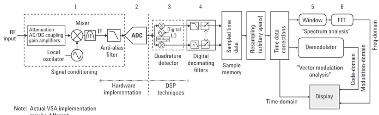
Figure 1-4 illustrates a general system block diagram of a VSA analyzer. Different manufacturers might use slightly different designs and, through DSP, many of the functions could occur at different places. Figure 1-4 shows a generalized diagram of the technique that Agilent uses in its VSAs. The VSA spectrum analysis measurement process includes these fundamental stages:
1. Signal conditioning with frequency translation 2. Analog-to-digital conversion
3. Quadrature detection
4. Digital filtering and resampling 5. Data windowing
6. FFT analysis (for vector modulation, blocks 5 and 6 are replaced with the demodulator block)
The first stage of the measurement process is called signal conditioning. This stage includes several important functions that condition and optimize the signal for the analog-to-digital conversion and FFT analysis. The first function is AC and DC coupling. This option is necessary if you need to remove unwanted DC biases in the measurement setup. Next, the signal is either amplified or attenuated for optimal signal level into the mixer. The mixer stage provides frequency translation, or RF-to-IF downconversion, and mixes the signal down to the final IF. This operation is the same as the superheterodyne function of the swept-tuned analyzer and extends FFT analysis capabilities through microwave. In practice, it may take several downconversion stages to reach the final IF frequency. Some analyzers provide external IF input capability; by providing your own IF, you can extend the upper frequency range of the analyzer to match a receiver you provide.
ADC
Sampled time data
Anti-alias filter Quadrature detector FFT Local oscilator RF input Demodulator DSP techniques IF Sample memory Digital decimating filters Display "Vector modulation analysis" "Spectrum analysis"
Note: Actual VSA implementation may be different.
Digital LO
Resampling (arbitary spans)
Window Time-domain Freq-domain Modulation-domain Code-domain Hardware implementation IF Attenuation AC/DC coupling gain amplifiers T
ime data corrections
Mixer 1 2 3 4 5 6 Signal conditioning 90 degs Q I
The final stage of the signal conditioning process is extremely important to a sampled system and FFT analysis; signal alias protection. The anti-alias filter performs this function. An analyzer that does not have adequate protection from aliasing may show frequency components that are not part of the original signal. The sampling theorem states that if the signal is sampled at a rate greater than 2 times the highest significant frequency component present in the signal, the sampled signal can be reconstructed exactly. The minimum acceptable sample rate is called the Nyquist rate. Thus,
fs> 2 (fmax)
where fs = sample rate
fmax= highest frequency component
If the sampling theorem is violated, “aliasing” error products can result. Therefore, to prevent alias products for a given maximum frequency, there must not be significant signal energy above 1/2 the sample rate. Figure 1-5 shows a set of sample points, which fit two different waveforms. The higher-frequency waveform violates the sampling theorem. Unless an anti-alias filter is used, the two frequencies will be indistinguishable when processed digitally.
To prevent aliasing, two conditions must be satisfied:
1. The input signal to the digitizer/sampler must be band limited. In other words, there must exist a maximum frequency (fmax) above which no frequency components are present.
2. The input signal must be sampled at a rate that satisfies the sampling theorem.
The solution to the aliasing problem seems simple enough. First you select the maximum frequency (fmax) that the analyzer will measure, then make sure the sampling frequency (fs) is twice that frequency. This step satisfies condition number 2 and makes sure that the analyzer can accurately measure the frequencies of interest. Next you insert a low-pass filter (an anti-aliasing filter) to remove all frequencies above fmax, thus ensuring that the
measurement will exclude all frequencies except those you are interested in. This step satisfies condition number 1 and makes sure the signal is band limited.
Reconstructed "alias" signal Actual signal ADC sample points fs ff X(f) f
(a) Aliasing in the time-domain (b) Aliasing in the frequency-domain Unwanted frequency components are folded onto the spectrum below cutoff.
recovered alias spectrum follows dashed line. fs 0 ( /f s 2)
Figure 1-5. Aliasing products occur when the signal is undersampled. Undesirable frequencies appear under the alias of another (baseband) frequency
There are two factors that complicate this simple anti-aliasing solution. The first, and easiest to address, is that the anti-alias filter has a finite roll off rate. As shown in figure 1-6, there is a transition band in practical filters between the passband and stopband. Frequencies within the transition band could produce alias frequencies. To avoid these alias products, the filter cutoff must be below the theoretical upper frequency limit of fsdivided by 2. An easy solution to this problem is to oversample (sample above the Nyquist rate). Make the sampling frequency slightly above 2 times fmaxso that it is twice the frequency at which the stopband actually starts, not twice the frequency you are trying to measure. Many VSA implementations use a guard band to protect against displaying aliased frequency components. The FFT computes the spectral components out to 50% of fs(equivalently fs/2). A guard band, between approximately 40% to 50% of fs(or fs/2.56 to fs/2), is not displayed because it may be corrupted by alias components. However, when the analyzer computes the inverse FFT, the signals in the guard band are used to provide the most accurate time-domain results. The high-roll-off-rate filter, combined with the guard band, suppresses potential aliasing components, attenuating them well below the noise floor of the analyzer.
The second complicating factor in alias protection (limited frequency resolution) is much harder to solve. First, an anti-alias filter that is designed for wide frequency spans (high sample rates) is not practical for measuring small resolution bandwidths for two reasons; it will require a substantial sample size (memory allocation) and a prohibitively large number of FFT computations (long measurement times). For example, at a 10 MHz sample rate, a 10 Hz resolution bandwidth measurement would require more than a 1 million point FFT, which translates into large memory usage and a long measurement time. This is unacceptable because the ability to measure small resolution bandwidths is one of the main advantages of the VSA. One way of increasing the frequency resolution is by reducingfs, but this is at the expense of reducing the upper-frequency limit of the FFT and ultimately the analyzer bandwidth. However, this is still a good approach because it allows you to have control over the resolution and frequency range of the analyzer. As the sample rate is lowered, the cut-off frequency of the anti-alias filter must also be lowered, otherwise aliasing will occur. One possible solution would be to provide an anti-aliasing filter for every span, or a filter with selectable cutoff frequencies. Implementing this scheme with analog filters would be difficult and cost prohibitive, but it is possible to add additional anti-alias filters digitally through DSP.
Band limited
analog signal ADC Wideband
input signal
Guard band
fs / 2.56
Passband Transition Stopband
Anti-alias filter ( ) (fs / 2)
f
Figure 1-6. The anti-alias filter attenuates signals above fs/2. A guard band between 40% to 50% of fsis not displayed
Digital decimating filtersand resamplingalgorithms provide the solution to the limited frequency resolution problem, and it is the solution used in Agilent VSAs. Digital decimating filters and resampling perform the operations necessary to allow variable spans and resolution bandwidths. The digital decimating filters simultaneously decrease the sample rate and limit the bandwidth of the signal (providing alias protection). The sample rate into the digital filter is fs; the sample rate out of the filter is fs/n, where “n” is the decimation factor and an integer value. Similarly, the bandwidth at the input filter is “BW,” and the bandwidth at the output of the filter is “BW/n”. Many implementations perform binary decimation (divide-by-2 sample rate reduction), which means that the sample rate is changed by integer powers of 2, in 1/(2n) steps (1/2, 1/4, 1/8...etc). Frequency spans that result from “divide by 2n” are called cardinal spans. Measurements performed at cardinal spans are typically faster than measurements performed at arbitrary spans due to reduced DSP operations.
The decimating filters allow the sample rate and span to be changed by powers of two. To obtain an arbitrary span, the sample rate must be made infinitely adjustable. This is done by means of a resampling or interpolation filter, which follows the decimation filters. For more details regarding resampling and interpolation algorithms, refer to the Referencessection at the end of this application note.
Even though the digital and resampling filters provide alias protection while reducing the sample rate, the analog anti-alias filter is still required, since the digital and resampling filters are, themselves, a sampled system which must be protected from aliasing. The analog anti-alias filter protects the analyzer at its widest frequency span with operation at fs. The digital filters follow the analog filter and provide anti-alias protection for the narrower, user-specified spans.
The next complication that limits the ability to analyze small resolution bandwidths is caused by a fundamental property of the FFT algorithm itself; the FFT is inherently a baseband transform. This means that the frequency range of the FFT starts from 0 Hz (or DC) and extends to some maximum frequency, fsdivided by 2. This can be a significant limitation in measurement situations where a small frequency band needs to be analyzed. For example, if an analyzer has a sample rate of 10 MHz, the frequency range would be 0 Hz to 5 MHz (fs/2). If the number of time samples (N) were 1024, the frequency resolution would be 9.8 kHz (fs/N). This means that frequencies closer than 9.8 kHz could not be resolved.
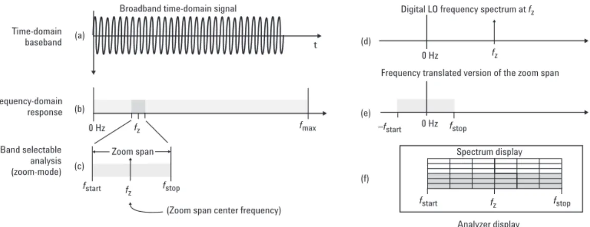
As just mentioned, you can control the frequency span by varying the sample rate, but the resolution is still limited because the start frequency of the span is DC. The frequency resolution can be arbitrarily improved, but at the expense of a reduced maximum frequency. The solution to these limitations is a process called band selectable analysis, also known as zoom operation or zoommode. Zoom operation allows you to reduce the frequency span while maintaining a constant center frequency. This is very useful because it allows you to analyze and view small frequency components away from 0 Hz. Zooming allows you to focus the measurement anywhere within the analyzers frequency range (Figure 1-7).
Zoom operation is a process of digital quadrature mixing, digital filtering, and decimating/resampling. The frequency span of interest is mixed with a complex sinusoid at the zoom span center frequency (fz), which causes that frequency span to be mixed down to baseband. The signals are filtered and decimated/resampled for the specified span, all out-of-band frequencies removed. This is the band-converted signal at IF (or baseband) and is sometimes referred to as “zoom time” or “IF time”. That is, it is the time-domain representation of a signal as it would appear in the IF section of a receiver. Zoom measurements are discussed further in the “Time-domain display” section near the end of this chapter.
Sample memory
The output of the digital decimating filters represents a bandlimited, digital version of the analog input signal in time-domain. This digital data stream is captured in sample memory (Figure 1-4). The sample memoryis a circular FIFO (first in, first out) buffer that collects individual data samples into blocks of data called time records, to be used by the DSP for further data processing. The amount of time required to fill the time record is analogous to the initial settling time in a parallel-filter analyzer. The time data collected in sample memory is the fundamental data used to produce all measurement results, whether in the frequency domain, time domain, or modulation domain.
Time domain data corrections
To provide more accurate data results, many VSAs implement time data correction capability through an equalization filter. In vector analysis, the accuracy of the time data is very important. Not only is it the basis for all of the demodulation measurements, but it is also used directly for measurements such as instantaneous power as a function of time. Correcting the time data is the last step in creating a nearly ideal bandlimiting signal path. While the digital filters and resampling algorithms provide for arbitrary bandwidths (sample rates and spans), the time-domain corrections determine the final passband characteristic of the signal path. Time-domain corrections would be unnecessary if the analog and digital signal paths could be made ideal. Time-domain corrections function as an equalization filter to compensate for passband imperfections. These imperfections come from many sources. The IF filters in the RF section, the analog anti-aliasing filter, the decimating filters, and the resampling filters all contribute to passband ripple and phase nonlinearities within the selected span.
Broadband time-domain signal
fmax t 0 Hz Zoom span fstop fstart Time-domain baseband Frequency-domain response Band selectable analysis (zoom-mode)
(Zoom span center frequency)
0 Hz fstop –fstart 0 Hz fstop fstart Spectrum display (a) (b) (d) (e) (c) (f) Analyzer display Digital LO frequency spectrum at fz
Frequency translated version of the zoom span
fz
fz
fz
fz
Figure 1-7. Band-selectable analysis (or zoommode): (a) measured broadband signal, (b) spectrum of the measured signal, (c) selected zoomspan and center frequency,
(d) digital LO spectrum (@ zoomcenter frequency), (e) frequency span mixed down to baseband, (f) display spectrum annotation is adjusted to show the correct span and center frequency
The design of the equalization filter begins by extracting information about the analog signal path from the self-calibration data based on the instrument’s configuration. This is the data used to produce the frequency-domain correction output display. Once the analog correction vector has been computed, it is modified to include the effects of the decimating and resampling filters. The final frequency response computations cannot be performed until after you have selected the span, because that determines the number of decimating filter stages and resampling ratio. The composite correction vector serves as the basis for the design of the digital equalization filter that is applied to the time data.
Data windowing - leakage and resolution bandwidth
The FFT assumes that the signal it is processing is periodic from time record to time record. However most signals are not periodic in the time record and a discontinuity between time records will occur. Therefore, this FFT assumption is not valid for most measurements, so it must be assumed that a discontinuity exists. If the signal is not periodic in the time record, the FFT will not estimate the frequency components accurately. The resultant effect is called leakage and has the affect of spreading the energy from a single frequency over a broad range of frequencies. Analog swept-tuned spectrum analyzers will produce similar amplitude and spreading errors when the sweep speed is too fast for the bandwidth of the filter.
Data windowing is the usual solution to the leakage problem. The FFT is not the cause of the error; the FFT is generating an “exact” spectrum for the signal in the time record. It is the non-periodic signal characteristics between time records that cause the error. Data windowing uses a window function to modify the time-domain data by forcing it to become periodic in the time record. In effect, it forces the waveform to zero at both ends of the time record. This is accomplished by multiplying the time record by a weighted window function. Windowing distorts the data in the time domain to improve accuracy in the frequency domain. See Figure 1-8.
Discontinuities in the time-record
Original signal Sampled
time record Windowfunction
Modified waveform Reduced leakage spectrum True spectrum f Spectrum with leakage f Log dB Log dB X =
Figure 1-8. Window functions reduce the leakage errors in the frequency domain by modifying the time domain waveform
Analyzers automatically select the appropriate window filter based on assumptions of the user’s priorities, derived from the selected measurement type. However, if you want to manually change the window type, VSAs usually have several built-in window types that you can select from. Each window function, and the associated RBW filter shape, offers particular advantages and disadvantages. A particular window type may trade off improved amplitude accuracy and reduced “leakage” at the cost of reduced frequency resolution. Because each window type produces different measurement results (just how different depends on the characteristics of the input signal and how you trigger on it), you should carefully select a window type appropriate for the measurement you are trying to make. Table 1-1 summarizes four common window types and their uses.
Table 1-1. Common window types and uses
Window Common uses
Uniform (rectangular, boxcar) Transient and self-windowing data
Hanning General purpose
Gaussian top High dynamic range
Flat top High amplitude accuracy
The window filter contributes to the resolution bandwidth
In traditional swept-tuned analyzers, the final IF filter determines the resolution bandwidth. In the FFT analyzers, the window type determines the resolution bandwidth filter shape. And the window type, along with the time-record length, determines the width of the resolution bandwidth filter. Therefore, for a given window type, a change in resolution bandwidth will directly affect the time-record length. Conversely, any change to time-record length will cause a change in resolution bandwidth as shown in the following formula:
RBW = normalized ENBW / T where ENBW = equivalent noise bandwidth
RBW = resolution bandwidth T = time-record length
Equivalent noise bandwidth (ENBW) is a figure of merit that compares the window filter to an ideal, rectangular filter. It is the equivalent bandwidth of a rectangular filter that passes the same amount (power) of white noise as the window. Table 1-2 lists the normalized ENBW values for several window types. To compute the ENBW, divide the normalized ENBW by the time-record length. For example, a Hanning window with a 0.5 second time-record length would have an ENBW of 3 Hz (1.5 Hz-s/0.5 s).
Table 1-2. Normalized ENBW values
Window type Normalized ENBW
Flat Top 3.819 Hz-s Gaussian top 2.215 Hz-s
Hanning 1.500 Hz-s
Fast Fourier transform (FFT) analysis
The signal is now ready for the FFT algorithm, but the way the FFT operates on the time-sampled data is not an intuitive process. The FFT is a record-oriented algorithm and operates on sampled data in a special way. Rather than acting on each data sample as the ADC converts it, the FFT waits until a number of samples (N) have been obtained (called a time record), then transforms the complete block. See Figure 1-9. In other words, a time record N samples long, is the input to the FFT, and the frequency spectrum N samples long, is the output.
The speed of the FFT comes from the symmetry or repeated sample values that fall out of restricting N to powers of 2. A typical record length for FFT analysis is 1024 (210) sample points. The frequency spectrum produced by
the FFT is symmetrical about the sample frequency fs/2 (this value is called the folding frequency,ff). Thus, the first half of the output record contains redundant information, so only the second half is retained, sample points 0 thru N/2. This implies that the effective length of the output record is (N/2) + 1. You must add 1 to N/2 because the FFT includes the zero line, producing outputs from 0 Hz thru N/2 Hz inclusive. These are complex data
points that contain both magnitude and phase information.
In theory, the output of the FFT algorithm is (N/2) +1 frequency points, extending from 0 Hz to ff. In practice however, a guard band is used for alias protection, so not all of these points are normally displayed. As mentioned earlier, a guard band (between approximately 40% to 50% of fs) is not displayed because it may be corrupted by alias components. For example, for a record length of 2048 samples, which produces 1025 unique complex frequency points, only 801 may actually be displayed.
.. .. .. . .. .. .. . . ... . . . ADC FFT
N = Number of sample points (*powers of 2) Sampling
fs = Sampling frequency
(sampling rate) = (N/2) + 1
Spectrum display
n = Number of lines (or bins)
∆ t
T
= N x t = 1/ f
T = Time record length f= Frequency step = 1/T = fs /N t = 1/fs= Sample time ∆ f 0 0 N Window Time record Time records 1 2 ...n Time record Frequency range Lines (N/2) 0 (fs/2) Samples fs N/fs 0 .
These frequency domain points are called lines, or bins, and are usually numbered from 0 to N/2. These bins are equivalent to the individual filter/detector outputs in a bank-of-filters analyzer. Bin 0 contains the DC level present in the input signal and is referred to as the DC bin. The bins are equally spaced in frequency, with the frequency step (∆f ) being the reciprocal of the measurement time-record length (T). Thus, ∆f = 1/T. The length of the time record (T) can be determined from the sample rate (fs) and the number of sample points (N) in the time record as follows: T = N/fs. The frequency ( fn) associated with each bin is given by:
fn= nfs/N where n is the bin number
The frequency of the last bin contains the highest frequency,fs/2. Therefore, the frequency range of an FFT is 0 Hz to fs/2. Note that the highest FFT range is notfmax, which is the upper-frequency limit of the analyzer, and may not be the same as the highest bin frequency.
Real-time bandwidth
Because the FFT analyzer cannot compute a valid frequency-domain result until at least one time record is acquired, the time-record length determines how long an initial measurement will take. For example, a 400-line measurement using a 1 kHz span requires a 400 ms time record; a 3200-line measurement requires a 3.2 s time record. This amount of data acquisition time is independent of the processing speed of the analyzer.
After the time record has been captured, processing speed does become an issue. The amount of time it takes to compute the FFT, format, and display the data results, determines the processing speed and display update rate. Processing speed can be important for two reasons. First, higher processing speeds can translate to decreased overall measurement time. Second, the ability of an analyzer to measure dynamic signals is a function of the processing speed. The performance indicator is the real-time bandwidth (RTBW), which is the maximum frequency span that can be continuously processed without missing any event in the input signal.
Time record 1 Time record 2 Time record 4 Time record 3 FFT 1 FFT 2 FFT 3 FFT 1 FFT 2 FFT 3 Time record 1 Time record 2 Time record 4 Time record 3 (b) Not real-time (a) Real time
These sections of the input signal are not processed
Time Digitized signal Digitized signal Input signal
Figure 1-10. (a) Processing is “real-time” when the FFT processing time is ≤the time-record length; no data is lost. (b) Input data is missed if the FFT processing time is greater than the time-record length
In the analyzer, RTBW is the frequency span at which the FFT processing time equals the time-record length. There is no gap between the end of one time record and the start of the next. See Figure 1-10. For any frequency spans less than RTBW, no input data is lost. However, if you increase the span past the real-time bandwidth, the record length becomes shorter than the FFT processing time. When this occurs, the time records are no longer contiguous, and some data will be missed.
Time-domain display
The VSA lets you view and analyze time-domain data. The displayed time-domain data may look similar to an oscilloscope display, but you need to be aware that the data you’re viewing may be quite different. The time-domain display shows the time-data just before FFT processing. See Figure 1-4. Many VSAs provide two measurement modes, baseband and zoom. Depending on the measurement mode, the time-domain data you are viewing will be very different.
Baseband mode provides time data similar to what you would view on a digital oscilloscope. Like the traditional digital signal oscilloscope (DSO), a VSA provides real-valued time data referenced to 0 time and 0 Hz (DC). However, the trace may appear distorted on the VSA, especially at high frequencies. This is because a VSA samples at a rate chosen to optimize FFT analysis, which, at the highest frequencies may only be 2 or 3 samples per period; great for the FFT, but not so good for viewing. In contrast, the DSO is optimized for time-domain analysis and usually oversamples the input. In addition, a DSO may provide additional signal reconstruction processing that enable the DSO to display a better time-domain representation of the actual input signal. Also, at maximum span, some signals (particularly square waves and transients) may appear to have excess distortion or ringing because of the abrupt frequency cut-off of the anti-alias filter. In this sense, DSOs are optimized for sample rate and time-domain viewing, not power accuracy and dynamic range.
In zoom(or band selectable) mode, which is typically the default mode
for a VSA, you are viewing the time waveform after it has been mixed and quadrature detected. Specifically, the time data you are viewing is the product of analog down conversion, IF filtering, digital quadrature mixing, and digital filtering/resampling, based on the specified center frequency and span. The result is a band-limited complex waveform that contains real and imaginary components and, in most cases, it looks different from what you would see on an oscilloscope display. This may be valuable information, depending on the intended use. For example, this could be interpreted as “IF time,” the time-domain signal that would be measured with an oscilloscope probing the signal in the IF section of a receiver. The digital LO and quadrature detector perform the zoommeasurement function. In zoomed measurements, the selected frequency span is mixed down to baseband at the specified center frequency (fcenter). To accomplish this, first the digital LO frequency is assigned the fcentervalue. Then the input signal is quadrature detected; it is multiplied or mixed with the sine
and cosine (quadrature) of the center frequency of the measurement span. The result is a complex (real and imaginary) time-domain waveform that is now referenced to fcenter, while the phase is still relative to the zero time trigger. Remember, the products of the mixing process are the sum and difference frequencies (signal – fcenterand signal + fcenter). So the data is further processed by the low-pass filters to select only the difference
frequencies. If the carrier frequency (fcarrier) is equal tofcenter, the
modulation results are the positive and negative frequency sidebands centered about 0 Hz. However, the spectrum displays of the analyzer are annotated to show the correct center frequency and sideband frequency values. Figure 1-11 shows a 13.5 MHz sinewave measured in both basebandand zoommode. The span for both measurements is 36 MHz and both start at 0 Hz. The number of frequency points is set to 401. The left-hand time trace shows a sinewave at its true period of approximately 74 ns (1/13.5 MHz). The right-hand time trace shows a sinewave with a period of 222.2 ns (1/4.5 MHz). The 4.5 MHz sinewave is the difference between the 18 MHz VSA center frequency and the 13.5 MHz input signal.
Summary
This chapter presented a primer on the theory of operation and measurement concepts using a vector signal analyzer (VSA). We went though the system block diagram and described each function as it related to the FFT measurement process. You learned that the implementation used by the VSA is quite different from the conventional analog, swept-tuned analyzer. The VSA is primarily a digital system incorporating an all-digital IF, DSP, and FFT analysis. You learned that the VSA is a test and measurement solution providing time-domain, frequency-domain, modulation-domain and code-domain signal analysis capabilities.
This chapter described the spectrum analysis capabilities of the VSA, implemented thorough FFT analysis. The fundamentals of FFT measurement theory and analysis were presented. The vector analysis measurement concepts and demodulator block, which include digital and analog modulation analysis, are described in Chapter 2.
Zoom: reference to center frequency fc LO = 18 MHz, fc = 18 MHz, span 36 MHz Real and imaginary values
Zoom signal = 4.5 MHz sinewave Baseband signal = 13.5 MHz sinewave
Baseband: reference to 0 Hz
LO = 0 Hz, fc = 18 MHz, span 36 MHz Real values only
(Signal to fc) = (13.5 MHz to 18 MHz) = – 4.5 MHz Real Digital LO = fc 90° phase shift Imaginary Quadrature detector (or Quadrature mixer)
f sample ADC 13.5 MHz sinewave
Ø
Chapter 2
Vector Modulation
Analysis
Introduction
Chapter 1 was a primer on vector signal analyzers (VSA) and discussed VSA measurement concepts and theory of operation. It also described the frequency-domain, spectrum analysis measurement capability of the VSA, implemented through fast Fourier transform (FFT) analysis. This chapter describes the vector-modulation analysis and digital-modulation analysis measurement capability of the VSA. Some swept-tuned spectrum analyzers can also provide digital-modulation analysis by incorporating additional digital radio personality software. However, VSAs typically provide more measurement flexibility in terms of modulation formats and demodulator configuration, and provide a larger set of data results and display traces. The basic digital-modulation analysis concepts described in this chapter can also apply to swept-tuned analyzers that have the additional digital-modulation analysis software.
The real power of the VSA is its ability to measure and analyze vector-modulated and digitally vector-modulated signals. Vector-modulation analysis means the analyzer can measure complex signals, signals that have a real and imaginary component. Since digital communications systems use complex signals (I-Q waveforms), vector-modulation analysis is required to measure digitally-modulated signals. But vector-modulation analysis is not enough to measure today’s complicated digitally-modulated signals. You also need digital-modulation analysis. Digital-modulation analysis is needed to demodulate the RF modulated carrier signal into its complex components (the I-Q waveforms) so you can apply vector-modulation analysis. Vector modulation analysis provides the numerical and visual tools to help quickly identify and quantify impairments to the I-Q waveforms. Digital-modulation analysis is also needed to detect and recover the digital data bits.
Digital demodulation also provides modulation quality measurements. The technique used in Agilent VSAs (described later in this chapter) can expose very subtle signal variations, which translates into signal quality information not available from traditional modulation quality measurement methods. Various display formats and capabilities are used to view the baseband signal characteristics and analyze modulation quality. The VSA offers traditional display formats such as I-Q vector, constellation, eye, and trellis diagrams. The symbol/error summary table shows the actual recovered bits and valuable error data, such as error vector magnitude (EVM), magnitude error, phase error, frequency error, rho, and I-Q offset error. Other display formats, such as magnitude/phase error versus time, magnitude/phase error
versus frequency, or equalizationallow you to make frequency response
and group delay measurements or see code-domain results. This is only a representative list of available display formats and capabilities. Those available in a VSA are dependent upon analyzer capability and the type of digital-modulation format being measured.
The VSA, with digital modulation provides measurement support for multiple digital communication standards, such as GSM, EDGE, W-CDMA, and cdma2000. Measurements are possible on continuous or burst carriers (such as TDMA), and you can make measurements at baseband, IF, and RF locations throughout a digital communications system block diagram. There is no need for external filtering, coherent carrier signals, or symbol clock timing signals. The general-purpose design of the digital demodulator in the VSA also allows you to measure non-standard formats, allowing you to change user-definable digital parameters for customized test and analysis purposes.
Another important measurement tool that vector-modulation analysis provides is analog-modulation analysis. For example, the Agilent 89600 VSA provides analog-modulation analysis and produces AM, FM, and PM demodulation results, similar to what a modulation analyzer would produce, allowing you to view amplitude, frequency, and phase profiles versus time. These additional analog-demodulation capabilities can be used to troubleshoot particular problems in a digital communications transmitter. For example, phase demodulation is often used to troubleshoot instability at a particular LO frequency.
The remainder of this chapter contains additional concepts to help you better understand vector-modulation analysis, digital-modulation analysis, and analog-modulation analysis.
Vector modulation and digital modulation overview
Let’s begin our discussion by reviewing vector modulation and digital modulation. Digital modulation is a term used in radio, satellite, and terrestrial communications to refer to modulation in which digital states are represented by the relative phase and/or amplitude of the carrier. Although we talk about digital modulation, you should remember that the modulation is not digital, but truly analog. Modulation is the amplitude, frequency, or phase modification of the carrier in direct proportion to the amplitude of the modulating (baseband) signal. See Figure 2-1. In digital modulation, it is the baseband modulating signal, not the modulation process, that is in digital form.
Frequency Amplitude
Amplitude & phase Phase t t t t Digital baseband modulating signal Digital data 1 0 1 0
Figure 2-1. In digital modulation, the information is contained in the relative phase, frequency, or amplitude of the carrier
Depending on the particular application, digital modulation may modify amplitude, frequency, and phase simultaneously and separately. This type of modulation could be accomplished using conventional analog modulation schemes like amplitude modulation(AM), frequency modulation(FM), or
phase modulation(PM). However, in practical systems, vector modulation
(also called complex or I-Q modulation) is used instead. Vector modulation is a very powerful scheme because it can be used to generate any arbitrary carrier phase and magnitude. In this scheme, the baseband digital information is separated into two independent components: the I (In-phase) and Q
(Quadrature) components. These I and Q components are then combined to form the baseband modulating signal. The most important characteristic of I and Q components is that they are independent components (orthogonal). You’ll learn more about I and Q components and why digital systems use them in the following discussion.
An easy way to understand and view digital modulation is with the I-Q or vector diagram shown in Figure 2-2. In most digital communication systems, the frequency of the carrier is fixed so only phase and magnitude need to be considered. The unmodulated carrier is the phase and frequency reference, and the modulated signal is interpreted relative to the carrier. The phase and magnitude can be represented in polar or vector coordinates as a discrete point in the I-Q plane. See Figure 2-2. I represents the in-phase (phase reference) component and Q represents the quadrature (90° out of phase) component. You can also represent this discrete point by vector addition of a specific magnitude of in-phase carrier with a specific magnitude of quadrature carrier. This is the principle of I-Q modulation.
I (volts) Q (volts) (Q uadrature or imaginary part) (In-phase or real part) Q - value I - value
0 deg (carrier phase reference) (I ,Q )1 1
Magnitude
θ Phase
A discrete point on the I-Q diagram represents a digital state or symbol location 1
1 –1
–1
By forcing the carrier to one of several predetermined positions in the I-Q plane, you can then transmit encoded information. Each position or state (or transitions between the states in some systems) represents a certain bit pattern that can be decoded at the receiver. The mapping of the states or symbols at each symbol timing instant (when the receiver interprets the signal) on the I-Q plane is referred to as a constellation diagram. See Figure 2-3. A symbol represents a grouping of the digital data bits; they are symbolic of the digital words they represent. The number of bits contained in each symbol, or bits-per-symbol (bpsym), is determined by the modulation format. For example, binary phase shift keying (BPSK) uses 1 bpsym, quadrature phase shift keying (QPSK) uses 2 bpsym, and 8-state phase shift keying (8PSK) uses 3 bpsym. Theoretically, each state location on the constellation diagram should show as a single point, but a practical system suffers from various impairments and noise that cause a spreading of the states (a dispersal of dots around each state). Figure 2-3 shows the constellation or state diagram for a 16 QAM (16-state quadrature amplitude modulation) format; note that there are 16 possible state locations. This format takes four bits of serial data and encodes them as single amplitude/phase states, or symbols. In order to generate this modulation format, the I and Q carriers each need to take four different levels of amplitude, depending on the code being transmitted.
In digital modulation, the signal moves among a limited number of symbols or states. The rate at which the carrier moves between points in the constellation is called the symbol rate. The more constellation states that are used, the lower the required symbol rate for a given bit rate. The symbol rate is important because it tells you the bandwidth required to transmit the signal. The lower the symbol rate, the less bandwidth required for transmission. For example, the 16QAM format, mentioned earlier, uses 4 bits per symbol. If the radio transmission rate is 16 Mbps, then the symbol rate = 16 (Mbps) divided by 4 bits, or 4 MHz. This provides a symbol rate that is one-fourth the bit rate and a more spectrally efficient transmission bandwidth (4 MHz versus 16 MHz). For more detailed information about digital modulation, see the Referencessection at the end of this application note.
I
Q
Constellation or state diagram
16 QAM 0000 0001 0010 0011 0100 0101 0110 0111 1000 1001 1010 1011 1100 1101 1110 1111 –1 1 -1 1 (volts) 0 I Q 1V –1V 0 1V –1V 0 01 00
serial bit stream
t
t Symbol mapping to IQ voltages
t 1 2 3 4 symbol timing instants (volts) symbols state: 0100 symbol: 1 I = 1 V Q = 0.5 V 00 01 11 0111 01 00 10
Figure 2-3. Each position, or state, in the constellation diagram represents a specific bit pattern (symbol) and symbol time
I-Q modulator
The device used in digital communications to generate vector modulation is the I-Q modulator. The I-Q modulator puts the encoded digital I and Q baseband information onto the carrier. See Figure 2-4. The I-Q modulator generates signals in terms of I and Q components; fundamentally it is a hardware (or software) implementation of a rectangular to polar coordinate conversion.
The I-Q modulator receives the I and Q baseband signals as inputs and mixes them with the same local oscillator (LO). Thus, I and Q are both upconverted to the RF carrier frequency. The I information amplitude modulates the carrier producing the in-phasecomponent. The Q information amplitude modulates a 90-degree (orthogonal) phase shifted version of the carrier producing the quadraturecomponent. These two orthogonal modulated carrier signals are summed together producing the composite I-Q modulated carrier signal. The main advantage of I-Q modulation is the symmetric ease of combining independent signal components into a single, composite signal, and later splitting the composite signal into its independent component parts.
Signals that are separated by 90 degrees are known as being orthogonalto each other, or in quadrature. The quadrature relationship between I and Q signals means that these two signals are truly independent. They are two independent components of the same signal. While changes of the Q input certainly alter the composite output signal, they do not change the I component at all. Similarly, changes of the I input have no effect on the Q signal. 90 deg. phase shift (Q uadrature component) (In-phase component) Composite output signal (I-Q modulated carrier) Rectangular coordinates Polar coordinates Summing circuits I baseband Local oscillator (carrier frequency) Q baseband Σ
I-Q demodulator
As you can see in Figure 2-5, the I-Q demodulator is a mirror image of the I-Q modulator shown in Figure 2-4. The I-Q demodulator recovers the original I and Q baseband signals from a composite I-Q modulated input signal.
The first step in the demodulation process is to phase-lock the receiver LO to the transmitter carrier frequency. It is necessary that the receiver LO be phase-locked to the transmitter carrier (or mixer LO) to correctly recover the I and Q baseband components. Then, the I-Q modulated carrier is mixed with both an unshifted LO, and a 90 degree phase-shifted version of the LO, producing the original I and Q baseband signals or components. The I-Q demodulation process is fundamentally a polar to rectangular conversion. Normally, information cannot be plotted in a polar format and reinterpreted as rectangular values without doing a polar-to-rectangular conversion. See Figure 2-2. However, this conversion is exactly what is done by the in-phase and quadrature mixing processes performed by the I-Q demodulator.
Why use I and Q?
Digital modulation uses I and Q components because it provides a simple, efficient, and robust modulation method for generating, transmitting, and recovering digital data. Modulated signals in the I-Q domain provide many advantages:
1. The I-Q implementation provides a method to create complex signals (both phase and amplitude change). Instead of using phase modulation, which is nonlinear and difficult to do well, the I-Q modulator simply modulates the amplitude of the carrier and its quadrature in a linear manner. Mixers with wide modulation bandwidths and good linearity are readily available. To produce a complex modulated signal, you only need to generate the baseband I and Q components of the signal. One key advantage of I-Q modulators is that the same modulator can be used to generate a variety of modulations from digital formats to RF pulses, or even radar chirps, for example.
2. Demodulating the signal is also straightforward. Using an I-Q demodulator, it is simple, at least in principle, to recover the baseband signals.
3. Looking at a signal in the I-Q plane often gives good insights about the signal. Effects like cross talk, data skew, compression, and AM-to-PM distortion, which are hard to visualize otherwise, are easy to see.
Composite input signal (I-Q modulated carrier)
Local oscillator (phase locked to the carrier frequency) 90 deg. phase shift I baseband (In-phase component) Q baseband (Q uadrature component) Polar
coordinates Rectangularcoordinates
Power splitter
Digital RF communication system concepts
Figure 2-6 shows a generic, simplified block diagram of the basic
architecture of a digital RF communications system that uses I-Q modulation. By understanding the fundamental concepts of this system, the operation of the VSA with vector modulation analysis may also be understood. In Figure 2-6, the system blocks enclosed by the dashed box show sections of the communications transmitter and receiver that can be measured and analyzed by the VSA with vector modulation analysis.
Digital communication transmitter concepts
The communications transmitter begins with speech coding (assuming voice transmission) which is the process of quantizing the analog signal and converting it into digital data (digitization). Then, data compression is applied to minimize the data rate and increase spectral efficiency. Channel coding and interleaving are common techniques used to improve signal integrity by minimizing the effects of noise and interference. Extra bits are often sent for error correction, or as training sequences, for identification or equalization. These techniques can also make synchronization (finding the symbol clock) easier for the receiver. The symbol encoder translates the serial bit stream into the appropriate I and Q baseband signals, each corresponding to the symbol mapping on the I-Q plane for the specific system. The symbol clock represents the frequency and exact timing of the transmission of the individual symbols. At the symbol clock transitions, the transmitted carrier is at the correct I-Q (or magnitude/phase) value to represent a specific symbol (a specific point on the constellation). The time interval between individual symbols is the symbol clock period, the reciprocal is the symbol clock frequency. The symbol clock phase is correct when the symbol clock is aligned with the optimum instant to detect the symbols.
Transmitter Receiver AGC I I Decode bits Adaption/ process/ decompress Processing/ compression/ error correction Symbol encoder DAC I I Q Q IF LO RF LO Q Voice input Voice output Q IF filter Baseband filters Speech coding Baseband filters IQ modulator Upconverter Amplifier Power control ADC RF LO Down convert IFfilter ADC IF LO IQ demodulator
May not represent actual radio system block diagram
Reconstrution filter
Once the I and Q baseband signals have been generated, they are filtered (band limited) to improve spectral efficiency. An unfiltered output of the digital radio modulator occupies a very wide bandwidth (theoretically, infinite). This is because the modulator is being driven by baseband I-Q square waves with fast transitions; fast transitions in the time domain equate to wide frequency spectra in the frequency domain. This is an unacceptable condition because it decreases the available spectrum to other users and causes signal interference to nearby users, called adjacent-channel-power interference. Baseband filtering solves the problem by limiting the spectrum and restricting interference with other channels. In effect, the filtering slows the fast transitions between states, thereby limiting the frequency spectrum. Filtering is not without tradeoffs, however; filtering also causes degradation to the signal and data transmission.
The signal degradation is due to reduction of spectral content and the overshoot and finite ringing caused by the filters time (impulse) response. By reducing the spectral content, information is lost and it may make reconstructing the signal difficult, or even impossible, at the receiver. The ringing response of the filter may last so long so that it affects symbols that follow, causing intersymbol interference (ISI). ISI is defined as the extraneous energy from prior and subsequent symbols that interferes with the current symbol such that the receiver misinterprets the symbol. Thus, selecting the best filter becomes a design compromise between spectral efficiency and minimizing ISI. There is a common, special class of filters used in digital communication design called Nyquist filters. Nyquist filters are an optimal filter choice because they maximize data rates, minimize ISI, and limit channel bandwidth requirements. You will learn more about filters later in this chapter. To improve the overall performance of the system, filtering is often shared, or split, between the transmitter and the receiver. In that case, the filters must be as closely matched as possible and correctly implemented, in both transmitter and receiver, to minimize ISI. Figure 2-6 only shows one baseband filter, but in reality, there are two; one each for the I and Q channel. The filtered I and Q baseband signals are inputs to the I-Q modulator. The LO in the modulator may operate at an intermediate frequency (IF) or directly at the final radio frequency (RF). The output of the modulator is the composite of the two orthogonal I and Q signals at the IF (or RF). After modulation, the signal is upconverted to RF, if needed. Any undesirable frequencies are filtered out and the signal is applied to the output amplifier and transmitted.
Digital communications receiver concepts
The receiver is essentially an inverse implementation of the transmitter, but it is more complex to design. The receiver first downconverts the incoming RF signal to IF, then demodulates it. The ability to demodulate the signal and recover the original data is often difficult. The transmitted signal is often corrupted by such factors as atmospheric noise, competing signal interference, multipath, or fading.
The demodulation process involves these general stages: carrier frequency recovery (carrier lock), symbol clock recovery (symbol lock), signal decomposition to I and Q components (I-Q demodulation), I and Q symbol detection, bit decoding and de-interleaving (decode bits), decompressing (expansion to original bit stream), and finally, digital to analog conversion (if required).
The main difference between the transmitter and receiver is the need for carrier and symbol clock recovery. Both the symbol clock frequency and phase (or timing) must be correct in the receiver to demodulate the bits successfully and recover the transmitted information. For example, the symbol clock could be set to the correct frequency, but at the wrong phase. That is, if the symbol clock is aligned to the transitions between symbols, rather than the symbols themselves, demodulation will be unsuccessful. A difficult task in receiver design is to create carrier and symbol clock recovery algorithms. Some clock recovery techniques include measuring the modulation amplitude variations, or in systems with pulsed carriers, the power turn-on event can be used. This task can also be made easier when channel coding in the transmitter provides training sequences or synchronization bits.
VSA digital modulation analysis concepts and theory of operation
The VSA can be viewed as a measuring receiver. It is really an I-Q receiver employing techniques similar to most digital radio receivers for decoding digital modulations. However, the difference is that the VSA is designed for high accuracy parametric measurement and display of modulation characteristics. Moreover, the VSA is a measurement tool that can measure and analyze almost every aspect of a digital communications transmitter and receiver system.Figure 2-7 shows an Agilent 89600 VSA simplified system block diagram. You may notice that many of the VSA system blocks are analogous to the digital communication receiver shown in Figure 2-6. The RF input signal is downconverted, through several stages of superheterodyne mixing, to an IF that can be accurately digitized by the ADC. This digitized IF is then vector (quadrature) detected and digitally filtered; downconverted one last time to an I and Q baseband form (I-Q time data) and stored in RAM. From here, DSP algorithms demodulate the signal; recover the carrier and symbol clock and apply reconstructive filtering and decoding (recover the original bits). With this DSP software implementation, almost any modulation format can be demodulated.
The VSA implementation is different from a radio receiver. The VSA deals with the sampled signals on a block basis; the radio receiver processes data serially, in real time. When you supply the VSA with radio receiver parameters, the VSA synthesizes the receiver via processing in the DSP. It provides all the functions of a receiver, down to making analog waveforms. Because the signal has been virtually digitized, it can be post-processed and viewed in any of the time, frequency, or modulation domains.
ADC
IQ baseband time data
Anti-alias filter Quadrature detector, digital filter FFT LO RF input Demodulator
•
Digital demod•
Analog demod Sample memory Display Vector modulation analysis Spectrum analysisNote: Actual VSA implementation may be different. Digital LO Time-domain Freq-domain Modulation-domain Code-domain Analog IF Re-sampled, corrected, time data I Q Digital IF 90 °
Figure 2-7. The VSA demodulator performs vector signal analysis, including digital and analog modulation analysis
VSA digital demodulator
The heart of the digital demodulation process in the VSA is the digital demodulator. Figure 2-8 shows a simplified block diagram of the digital demodulator implementation used in the Agilent 89600 VSA. The digital demodulator is a general purpose demodulator that only requires a minimum of prior information about the input signal to perform demodulation, and can be used on a wide variety of modulation formats. The demodulator provides carrier lock, symbol clock recovery, and bit recovery (decodes the actual encoded 1s and 0s), and produces the I-Q measured waveforms. The demodulator also produces ideal I-Q waveforms that are synthesized from the actual recovered bits (called I-Q reference waveforms). The I-Q measured and I-Q reference waveforms are subtracted to produce I-Q error waveforms. The I-Q error waveforms are analyzed to generate the modulation quality data results, which can be viewed in various data formats and display outputs.
The demodulation process begins by configuring the demodulator. The demodulator must be configured to the specific digital modulation format to properly demodulate and analyze the signal. Most analyzers provide a set of standard presets, such as GSM, W-CDMA, cdma2000, or 802.11a/b/g, that automatically configure the demodulator for you. In those cases, you enter the center frequency, select a standard preset, and the analyzer can demodulate the signal. Some VSAs, like the Agilent 89600 VSA, give you additional capabilities through a general purpose, user-definable demodulator. This allows you to customize the demodulator configuration for non-standard formats or troubleshooting purposes. The demodulator block diagram shown in figure 2-8 shows the internal demodulator processes (enclosed in rectangular boxes) and the configuration parameters that you can set (enclosed by ovals or rounded rectangular boxes). The items enclosed by
Error vector time/spectrum IQ phase error IQ mag error EVM Mag error Phase error I/Q offset Amp droop SNR (QAM only) Shown in symbol table Symbol bits
(shown in symbol table) IQ ref time IQ meas time Meas
filter Freq error
(shown in symbol table)
Carrier and symbol lock Amp droop I/Q offset Symbol timing recovery /BT α Result length Compensation Center freq Clock adjust Symbol rate Pts per sym Sync word Sync position Ref filter Error calc I-Q time data BW filter Span Pulse detection Search length
Oval items require user input for demodulator configuration. Rounded rectangular items are user adjustable inputs.
– + IQ meas time IQ meas time IQ ref time Baseband filtering Symbol detector Reference generator Sync detector Σ