Two Chip Solution for
Brushless Motor Controller
Design
Motor control designers who wish to take advantage of the brushless DC motor’s unique attributes are faced with a difficult task. There are limited control ICs designed to decode data coming from Hall effect sensors, let alone perform all the ancillary functions such as forward/reverse selection, overcurrent shutdown, undervoltage lockout, overtemperature shutdown, and so forth. Using discrete components to include these functions is an alternative, but discretes often consume too much circuit board area, especially if the control unit is to be placed inside the motor housing.
Two linear ICs, combine to form a simple design, high performance system.
THE BRAINS
The system highlighted here is built with ON Semiconductor’s MC33035 and a support chip, the MC33039. Automotive grade parts are also available as NCV33035 and NCV33039. They are examples of ICs that dramatically simplify the design of brushless motor control systems and reduce required circuit board area and parts count. Added benefits are shorter design times and improved system performance.
The MC33035 is a 24−pin linear IC that can operate as the control center for a brushless DC motor control system. The main duty of the MC33035 is to decode the signals from the Hall effect sensors and generate logic for electronically commutating the motor. The commutation logic is internally fed into the six output drivers consisting of three open collector NPN transistors that drive the upper legs of the bridge and three totem pole drivers that control the lower bridge transistors. The open collector outputs can sink 50 mA; with some additional circuitry this allows control of
or P−channel MOSFETs if a simple interface is desired. Since the three lower totem pole outputs can source and sink 100 mA, they can drive power MOSFETs directly.
Fault Management
The MC33035 can detect and manage several types of faults. A common method of overcurrent detection is to tie the sources of the lower three transistors together and return them to the negative supply rail through a current sense resistor. The sense voltage, which is proportional to load current, is fed into a comparator internal to the MC33035. The comparator then feeds an RS Flip−Flop, which ensures that once an overcurrent condition is detected, the output drivers turn off the power transistors for the remainder of the oscillator cycle. Without the internal flip−flop, the overcurrent protection loop would rapidly cycle On and Off about the comparator’s threshold, causing excessive power transistor heating.
In addition to overcurrent management, the MC33035 provides undervoltage lockouts that terminate the drive to the output transistors if any of three conditions occur. The first is insufficient voltage to operate the IC. The second occurs when there is insufficient voltage to drive the power MOSFET gates. Finally, the output drivers turn off the power transistors when the MC33035 does not sustain its on board 6.25 V reference. An invalid set of Hall effect signals or excessive temperature will also cause shutdown.
Whenever any fault condition is present, an NPN transistor capable of sinking 16 mA pulls the Fault Output pin low. Potential uses of the Fault Output include alerting a microprocessor of a problem, lighting an LED, implementing a soft start feature to limit motor start up currents, or latching the system off at the first sign of a
APPLICATION NOTE
http://onsemi.com http://onsemi.com
http://onsemi.com
2
Control Features
The MC33035’s circuitry contains all but one of the major elements for closed loop speed control. The only piece lacking is one that monitors motor RPM and generates a signal proportional to motor speed, a function which traditionally has been the domain of a tachometer. Once provided with a motor speed signal, the MC33035’s high performance error amplifier and its internal oscillator form the last major links in the control loop.
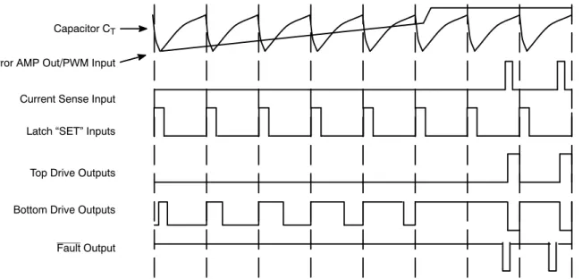
The MC33035’s on−board oscillator operates at a frequency set by an external R−C. Each cycle capacitor CT (Figure 1) is charged from the reference output through resistor RT and then rapidly discharged through an internal transistor. Figure 2 shows how the resulting sawtooth−
shaped waveform affects output pulse width.
The MC33035 has tremendous flexibility since it works well with various Hall effect sensor spacings and the most common brushless motor windings. An MC33035−based system can easily be altered to drive motors with either delta or wye connected three phase windings with 60 or 120 degree Hall effect sensor spacing.
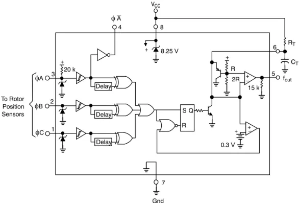
A companion IC, the MC33039, is a low cost, space saving alternative to a tachometer. At each positive or negative transition of the Hall effect sensors, the MC33039 generates a pulse with a fixed on time. The output signal can then be filtered to obtain a voltage proportional to motor speed. Design of an MC33035/39−based system should begin with setting the system timing, which originates in the MC33039.
Figure 1. MC33035 Representative Block Diagram 15 24 20 2 1 21 19 VM Top Drive Outputs Bottom Drive Outputs CB Current Sense Reference Input BB AB AT BT CT Q S R Oscillator Error Amp PWM Thermal Shutdown Reference Regulator Lockout Undervoltage Q R S Rotor Position Decoder Brake Input 60°/120°Select
Output Enable CT RT Vin 4 10 11 13 8 12 3 17 22 7 6 5 Forward/Reverse Faster Noninv. Input SA SC SB Sensor Inputs
Error Amp Out PWM Input Sink Only Positive True Logic With Hysteresis = Reference Output 16 Latch Latch 23 Gnd 14
9 Current Sense Input Fault Output 20 k 20 k 20 k 40 k 40 k 25 μA VCC VC 18 9.1 V 4.5 V 100 mV 40 k
Figure 2. The MC33035’s Pulse−Width Modulator Timing Diagram
Capacitor CT
Error AMP Out/PWM Input Current Sense Input Latch “SET” Inputs
Top Drive Outputs
Bottom Drive Outputs
http://onsemi.com
4 ASSEMBLING THE PIECES
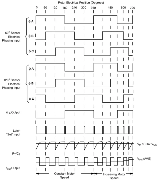
Figure 3 shows the MC33039 timing diagram, and Figure 4 shows its representative block diagram. Selection of timing components for the MC33039 is based on the desired maximum motor RPM. For the motor used in this application (Pittman ELCOM 5112), there are two electrical
degrees for every mechanical degree since the permanent magnet on the rotor has two pairs of poles. Therefore, for every mechanical revolution, each Hall−effect sensor delivers two pulses and the three sensors generate six pulses. The MC33039 generates 12, one for each rising and falling edge.
Rotor Electrical Position (Degrees)
0 60 120 180 240 300 360 480 600 720
Vth ≈0.67 VCC
Vout (AVG)
Constant Motor
Speed Increasing MotorSpeed
Figure 3. Timing Diagram of a Typical Three Phase, SIx Step Motor Application
φ A
φ B
φ C
φ A
φ B
φ C 60° Sensor
Electrical Phasing Input
120° Sensor Electrical Phasing Input
φ A Output
Latch “Set” Input
RT/CT
VCC
8 4
8.25 V
RT
CT
6
5 15 k +
+ +
+
+ −
+− 0.3 V
R
2R fout
S R
Q
7 Gnd Delay
Delay
Delay 1
2 3
To Rotor Position Sensors
20 k
φ A
φA
φB
φC
Figure 4. Representative Block Diagram of MC33039
For a given maximum motor speed, the output pulse width has a maximum limit. If we assume a maximum desired speed of 5000 RPM, which is about 83 revolutions per second, the MC33039 will generate 83 x 12, or 1000 pulses per second. The 1 kHz frequency dictates that the maximum pulse width must be less than 1 ms. From Figure 5, which is taken from
the MC33039’s data sheet, one can determine that R1 and C1 values of 43 kW and 22 nF result in a pulse width of 950 ms. To set the system PWM frequency, refer to the MC33035’s data sheet. There it shows that setting R2 and C2 to 5.1 kW and
0.01 mF gives a nominal pulse width modulation frequency of 24 kHz, just above the audible range.
CT = 220 nF
22 nF
2.2 nF
2.0 20 200
0.01 0.1 1.0 10 100
RT, TIMING RESISTOR (KW)
PW
, OUTPUT
PULSE WIDTH (ms)
t
Figure 5. fout Pulse Width versus Timing Resistor
VCC = 6.25 V
http://onsemi.com
6
Both inputs and the output of the MC33035’s error amplifier are accessible to accommodate various control methods. For open loop control, you can feed a reference signal proportional to desired speed into the error amplifier’s non−inverting input. The error amplifier is then configured as a unity gain voltage follower by connecting its inverting input to its output. The error amplifier’s output is then compared to the output of the oscillator to obtain a PWM signal proportional to desired motor speed − unless the control loop is overridden by an overcurrent or fault condition.
For closed loop control, one approach is to filter the MC33039’s output with a low pass filter to generate a voltage proportional to motor speed and feed the resulting signal into the inverting input of the MC33035’s comparator. A signal proportional to desired motor speed drives the non−inverting input, and the ratio of the input and feedback resistors R3 and R4 control gain. In this design, low pass filtering and generating the error signal are combined by using feedback capacitor, C3.
Ideally, the integrator/error amplifier should produce a ripple−free output even at low motor speeds. To do so at very low speeds reduces system response time, however. Component values must be adjusted according to the rotor’s mechanical time constant. In this particular application, the values 1 MWand 0.1 mF (t = 100 ms) give good dynamic response and stability.
When motor speed falls below the desired speed, the MC33035 increases the drive transistor duty cycle. When motor speed is greater than the desired speed, the duty cycle decreases. However, if the input signal abruptly demands a much lower speed, the duty cycle could fall to zero and the motor would coast to desired low speed. Therefore, since the MC33035 has no provision to dynamically brake the motor and thus control rapid deceleration, it is best suited for applications which have a large frictional load or those that do not require a controlled, abrupt deceleration. The schematic of a closed loop brushless motor control system is shown in Figure 6.
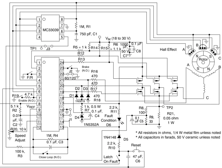
Figure 6. Typical 24 V Brushless Motor Drive (with 120 Degree Sensor Phasing)
* All resistors in ohms, 1/4 W metal film unless noted * All capacitors in farads, 50 V ceramic unless noted
47 mF, C6 Reset Latch On Fault 2.2 k, R10 1N4148 D5 R8, 100 R9, 33 TP2 0.1
mF C5
R21, 0.05 ohm
1 W
C A
S N B
Rotor
N S
C
A B
Hall Effect 0.1 mF
C8 VM (18 to 30 V)
R14 R15 = 1.1 kR6 mF, 50 V
C7 1M, R1
750 pF, C1
R5 = 1 k R12 R13 1 2 3 4 5 6 7 8 MC33039 TP1 J3 F/R J2 60/120 D3 Brake (N.O.) R16 470 470 R17 470 R18 D2 1N5819 J1 D4
1 k, 0.5 W R7
1N5352A 0.1 mF,
C4 2.2 k, R11 Fault Condition D6 D1
R19 4.7 k
Enable (N.O.) VREF 100 k, R3 Speed Adjust R20, 10 k
0.01 mF, C2
1M, R4 0.1 mF, C3
Close Loop (N.O.)
1 2 3 4 5 6 7 8 9 10 11 12 13 14 15 16 17 18 19 20 21 22 23 24 1000 5.1 k R2
Lower Gate Drive Circuit
The magnitude of the system voltage effects how one might deliver power to the MC33035 and generate the gate drive supply for the N−channel power MOSFETs. Here we are only concerned with two possible supply voltages, 12 V (a range of 9 to 16 V) and 24 V (18 to 30 V). Since the MC33035 has a 40 V rating, it can be powered directly from either system supply voltage if the supply is free of large voltage transients. In addition to an electrolytic capacitor a small filter capacitor (0.1 mF) located near the IC is recommended to reduce local spiking across the DC bus.
For reduced power dissipation in the IC, the MC33035 allows driving the three lower output transistors from a supply that is independent of the MC33035’s supply. Because the power transistors in this application example are MOSFETs, the only required drive current is that which is needed to charge and discharge each MOSFET’s gate-to-source and drain-to-gate capacitors. Since the charging current needed for the three P-channel MOSFETs is delivered directly from the DC bus, that charge is not included when sizing the impedance of the gate drive bus voltage.
Although the average gate current drawn by the MOSFETs is quite small, charging their input capacitances takes high peak currents. Therefore, the filter capacitor, C4, essentially supplies the entire turn-on current, and the capacitor is refreshed through resistor, R7. When the supply dips to its lowest specified value for a 24 V system (18 V), the dropping resistor has only three volts across it. Using a 1 kW resistor will provide plenty of current to keep the capacitor charged and supply at least 1 mA to the zener to ensure good regulation. At high supply voltages the resistor will see a voltage of 15 V, a current of 15 mA, and a power dissipation of about a quarter of a watt. Therefore, a 1/2 watt resistor should be adequate. That’s also a good power rating for the zener. For the 12 V supply, less voltage appears across the dropping resistor, so it can be a 1/4 watt device.
Capacitor C4 should be able to deliver the entire gate charge for a single cycle without a significant dip in its voltage. For 15 nC and a maximum allowable drop in voltage of 0.5 V, the capacitor should be 0.03 mFd. Since a MOSFET draws essentially no drive current after it has been turned on, the output duty cycle doesn’t significantly affect drive requirements. Only switching frequency and charge affect average current.
Filter capacitor C4 can be eliminated if the series resistor R7 is small enough to satisfy gate drive requirements at any instant. The cost is higher losses in the zener diode and series resistor, which is likely to require devices with greater power
substrate of the MC33035. Three Schottky diodes D1-3, one from each lower drive output to ground, are required if substrate current exceeds 50 mA.
Problems may also arise if the gate drive impedance of the three lower devices is unnecessarily low. If little or no resistance is placed between the IC and the MOSFET, the gate drive loop may cause ringing during gate voltage transitions. The gate drive loop may cause ringing during gate voltage transitions. Such ringing is amplified by the MOSFET and may cause unacceptably high levels of noise at the drain. The solution to the problem is to reduce the circuit’s Q by inserting a series gate resistor. The minimum required value depends on circuit parasitics, so it is difficult to give recommendations. However, the resistance required to keep switching losses reasonably low is usually much larger than the resistance required to eliminate oscillations. Typically values less than 62 ohms will cause oscillations.
There is a second reason to avoid very fast turn-on of the N-channels. When a lower device turns on, the P-channel in the upper leg of that same half bridge has been conducting current in its drain-source diode. Reverse recovery charge is swept out of the diode by the lower switch. If turn on speeds are high, large reverse recovery currents and rapid swings in drain-to-source voltage will produce EMI.
Upper Gate Drive Current
For standard MOSFETs it is desirable, but not absolutely necessary, to have 10 volts available to drive the gate. However, as drain currents decrease, the gate voltage needed to conduct those currents also falls. Depending on the device’s transfer characteristics and the desired load current, gate voltages in the 7 to 8 V range may be acceptable. In a 24 V system there is plenty of voltage available to drive the gate, so R5 and R6 are sized to ensure that the P-channel receives − 10 V of gate drive even when the supply voltage drops to 18 V.
R5, 12 and 13 govern charging of the P-channels’ input capacitances and thus control turn-on speed. Similarly, R6, R14 and R15 determine turn-off speed. Lowering the value of each resistor in the divider maintains the desired − 10 V gate drive and decreases the gate drive impedance at the expense of increased current and power dissipation in the resistors.
A common pitfall in the design of the P-channel drive is to assume that since the P-channel FETs are switching at the motor’s commutation frequency (a frequency much lower than the PWM frequency) they do not need the low impedance gate drive that the N-channel FETs require. What is often missed is that whenever the P−channel
http://onsemi.com
8
systems are especially prone to gate drive problems since the excursions in VDS are so large.
Avoiding shoot through currents is easy. First, slow the turn-on of the N-channels to limit impressed dv/dt’s; second, keep the P-channels’ gate drive impedance low, especially in the off-state. Adding capacitance across the P-channels’ gate-to-source (0.01 mF often works) is a simple way to give the gate drive a reservoir of charge that keeps the gate off when Cdg demands displacement current.
When a 12 V supply is used, the full supply voltage is impressed across the gate-to-source when the MOSFET is supposed to be on. This is done by shorting the pull down resistors, R5, R12 and R13. Since there is no longer any series resistance to limit gate current, turn-on speed will be much faster than turn-off speeds.
Overcurrent Sensing
The MC33035 has a comparator for detecting excessive load currents. A signal from a current sensing resistor common to all the N-channel sources is fed into Pin 9. The trip threshold is internally set to 100 mV. If a greater trip voltage is desired, the MC33035 allows connection of an additional offset voltage to Pin 15. In this design a 1 W, 0.05 W resistor R21 is used to sense current, and the sense voltage is attenuated by a voltage divider. The values chosen for the voltage divider, 100 W (R8 in Figure 6) for the upper resistor and 33 W (R9) for the lower, set the current trip to 8 A.
Putting a small capacitor (C5) on the comparator input is a good way to keep noise or currents such as reverse recovery spikes of freewheeling diodes from tripping the overcurrent comparator. It is easy to see that the DC gain of the network is set by the resistive divider, but the time constant may not be obvious at a glance. The transfer function for the resistive divider network and the capacitor is:
Vo Vi +
R9 R8)R9
1)C5 R8 R9R8)R9
where Vi is the voltage across the current sense resistor and
Vo is the voltage appearing at the input of the comparator.
Therefore, the time constant is equal to the parallel combination of R8 and R9 times C5. In this case τ is 2.4 ms (24 times 0.1 mF). Power MOSFETs are known to be able to withstand high surge currents, especially if their duration is less than 10 microseconds. Therefore, a time constant of this magnitude gives adequate protection.
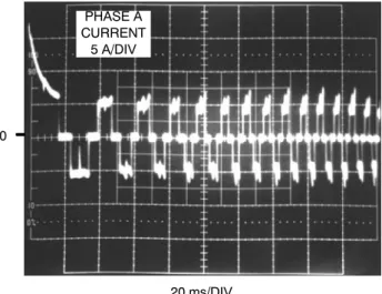
The benefit of over current protection is apparent in a comparison of Figures 7 and 8. In Figure 7, where no current
feedback is used, the start up current peak reaches 16 A, and in Figure 8, current is bounded by the 8 A limit.
Another potentially stressful operating condition occurs when the motor is required to abruptly change direction of rotation. If no overcurrent sensing is used, currents are limited only by the winding resistance and the on-resistance of the power MOSFETs.
20 ms/DIV PHASE A
CURRENT 5 A/DIV
0
Figure 7. Motor Start Up Current Without Overcurrent Protection
PHASE A CURRENT
5 A/DIV
20 ms/DIV
Figure 8. Motor Start Up Current With Overcurrent Protection
A third mode of operation that causes high currents is the brake mode. Upon application of the brake signal, all three bottom transistors are turned on, shorting the motor windings. Since current circulates between windings through the three N-channels and does not appear in the sense resistor, the MC33035 can not detect the high currents in the brake mode. Therefore, the MOSFETs must be sized to handle very large currents if the brake is used.
As Figure 9 shows, current peaks reach 35 A and last long enough to be of a reliability concern for the power transistors. Peak current is a function of the power transistor and winding resistances and the motor’s back EMF during braking. The time required for the current to decay depends on motor speed, motor winding resistance, frictional loading, and motor inertia. The photograph shows that current rings between windings until the energy stored in the spinning rotor is extinguished by dissipative elements.
Figure 9. Application of Brake Signal May Produce Large Fault Currents
0
MOTOR WINDING CURRENT
10 A/ DIV
20 ms
Fault Indicator and Overcurrent Latch
Should any of the fault conditions occur, the Fault Output, Pin 14, is pulled low. Having an LED to indicate a fault is a handy diagnostic tool. To maintain roughly 1 mA in the LED, R11 is 2.2 kW in a 24 V system and 1 kW if the supply is 12 V.
Upon detection of a fault, it is often desirable to inhibit any further pulsing of the output transistors. This can be accomplished by tying the Fault Output to Pin 7, the Enable pin. A delay in the latch can be implemented by adding C6. The time constant of R10 and C6 fixes the delay before the system latches.
BIBLIOGRAPHY
Alberkrack, J. “A New Brushless Motor Controller.” Proceedings of SATECH 1986.
“Brushless DC Motor Control Handbook.” Inland Motor Corp., 4020 E. Inland Road, Sierra Vista, AZ 85635. Gauen, K. and W. Schultz. “Proper Testing Can Maximize Performance in Power MOSFETs.” EDN, May 14, 1987.
Gauen, K. “Understanding the Power MOSFET’s Input Characteristics.” Motorola Article Reprint AR196. Katti, A. “Analysis of ECPM Motors with Torque Rolloff Due to Armature Reaction.” PCIM, October 1988. Saner, F. “Pittman Servo Motor Application Notes.” Pittman, Harleysville, PA 19438.
ON Semiconductor and are registered trademarks of Semiconductor Components Industries, LLC (SCILLC). SCILLC reserves the right to make changes without further notice to any products herein. SCILLC makes no warranty, representation or guarantee regarding the suitability of its products for any particular purpose, nor does SCILLC assume any liability arising out of the application or use of any product or circuit, and specifically disclaims any and all liability, including without limitation special, consequential or incidental damages. “Typical” parameters which may be provided in SCILLC data sheets and/or specifications can and do vary in different applications and actual performance may vary over time. All operating parameters, including “Typicals” must be validated for each customer application by customer’s technical experts. SCILLC does not convey any license under its patent rights nor the rights of others. SCILLC products are not designed, intended, or authorized for use as components in systems intended for surgical implant into the body, or other applications