LTC4415
1
4415fa
Typical applicaTion
FeaTures
DescripTion
Dual 4A Ideal Diodes with
Adjustable Current Limit
The LTC®4415 contains two monolithic PowerPath idealdiodes, each capable of supplying up to 4A with typical forward conduction resistance of 50mΩ. The diode voltage drops are regulated to 15mV during forward conduction at low currents, extending the power supply operating range and ensuring no oscillations during supply switchover. Less than 1µA of reverse current flows from OUT to IN making this device well suited for power supply ORing applications.
The two ideal diodes are independently enabled and prioritized using inputs EN1 and EN2. The output current limits can be adjusted independently from 0.5A to 4A using resistors on the CLIM pins. Furthermore, the ideal diode currents can be monitored via CLIM pin voltages. Open-drain status pins indicate when the ideal diodes are forward conducting. When the die temperature approaches thermal shutdown, or if the output load exceeds the cur-rent limit threshold, the corresponding warning pins are pulled low.
Prioritized Power Supply ORing
applicaTions
n Dual 50mΩ Monolithic Ideal Diodes n 1.7V to 5.5V Operating Range
n Up to 4A Adjustable Current Limit for Each Diode n Low Reverse Leakage Current (1µA Max)
n 15mV Forward Drop in Regulation
n Smooth Switchover in Diode ORing n Load Current Monitor
n Precision Enable Thresholds to Set Switchover n Soft-Start to Limit Inrush Current on Start-Up n Status Pins to Indicate Forward Diode Conduction n Current and Thermal Limit with Warning
n Thermally Enhanced 16-Lead MSOP and DFN
(3mm × 5mm) Packages
n High Current PowerPath™ Switch n Battery and Wall Adapter Diode ORing n Backup Battery Diode ORing
n Logic Controlled High Current Power Switch n Supercapacitor ORing
n Multiple Battery Sharing
L, LT, LTC, LTM, Linear Technology and the Linear logo are registered trademarks and PowerPath is a trademark of Linear Technology Corporation. All other trademarks are the property of their respective owners.
IDEAL IDEAL LTC4415 GND EN1 4415 TA01a 4.7µF TO LOAD 100k 21.5k 124Ω 124Ω CLIM1 CLIM2 STAT1 WARN1 WARN2 STAT2 EN2 IN2 IN1 OUT1 OUT2 PRIMARY POWER SOURCE SECONDARY POWER SOURCE +
FORWARD VOLTAGE DROP (mV) 0
LOAD CURRENT (A)
3 4 400 4415 TA01b 2 1 0 100 200 300 500 CURRENT LIMIT LTC4415 RON = 50mΩ SCHOTTKY DIODE MBRS410E Forward Characteristics of LTC4415 vs MBRS410E Schottky
LTC4415
2
4415fa
absoluTe MaxiMuM raTings
IN1, IN2, OUT1, OUT2, CLIM1, CLIM2,STAT1, STAT2, WARN1, WARN2 Voltage ... –0.3V to 6V EN1, EN2 Voltage ... –0.3V to Max (VINx, VOUTx) Operating Junction Temperature Range
(Notes 3, 4) ...–40°C to 125°C (Note 1) 16 15 14 13 12 11 10 9 17 GND 1 2 3 4 5 6 7 8 OUT1* OUT1* STAT1 WARN1 WARN2 STAT2 OUT2* OUT2* IN1* IN1* EN1 CLIM1 CLIM2 EN2 IN2* IN2* TOP VIEW DHC PACKAGE VARIATION A 16-LEAD (5mm × 3mm) PLASTIC DFN TJMAX = 125°C, θJA = 43°C/W
EXPOSED PAD (PIN 17) IS GND, MUST BE SOLDERED TO PCB *ADJACENT PINS ON THE FOUR CORNERS ARE FUSED TOGETHER
1 2 3 4 5 6 7 8 IN1* IN1* EN1 CLIM1 CLIM2 EN2 IN2* IN2* 16 15 14 13 12 11 10 9 OUT1* OUT1* STAT1 WARN1 WARN2 STAT2 OUT2* OUT2* TOP VIEW 17 GND MSE PACKAGE 16-LEAD PLASTIC MSOP TJMAX = 125°C, θJA = 35°C/W TO 40°C/W
EXPOSED PAD (PIN 17) IS GND, MUST BE SOLDERED TO PCB *ADJACENT PINS ON THE FOUR CORNERS ARE FUSED TOGETHER INTERNALLY.
pin conFiguraTion
orDer inForMaTion
LEAD FREE FINISH TAPE AND REEL PART MARKING* PACKAGE DESCRIPTION TEMPERATURE RANGE
LTC4415EDHC#PBF LTC4415EDHC#TRPBF 4415 16-Lead (5mm × 3mm) Plastic DFN –40°C to 125°C
LTC4415IDHC#PBF LTC4415IDHC#TRPBF 4415 16-Lead (5mm × 3mm) Plastic DFN –40°C to 125°C
LTC4415EMSE#PBF LTC4415EMSE#TRPBF 4415 16-Lead Plastic MSOP –40°C to 125°C
LTC4415IMSE#PBF LTC4415IMSE#TRPBF 4415 16-Lead Plastic MSOP –40°C to 125°C
Consult LTC Marketing for parts specified with wider operating temperature ranges. *The temperature grade is identified by a label on the shipping container. Consult LTC Marketing for information on non-standard lead based finish parts.
For more information on lead free part marking, go to: http://www.linear.com/leadfree/ For more information on tape and reel specifications, go to: http://www.linear.com/tapeandreel/
Storage Temperature Range ... –65°C to 150°C Peak Reflow Temperature ...260°C
LTC4415
3
4415fa
elecTrical characTerisTics
The l denotes the specifications which apply over the specified operatingjunction temperature range, otherwise specifications are at TA = 25°C (Notes 2, 3). VIN1 = VIN2 = 3.6V, RCLIM = 250Ω, unless otherwise
specified.
SYMBOL PARAMETER CONDITIONS MIN TYP MAX UNITS
VIN1, VOUT1, VIN2, VOUT2
Operating Supply Range At Least One Input/Output Must Be in This Range l 1.7 5.5 V
VUVLO Undervoltage Lockout VINx Rising
Hysteresis
l 1.63
55 1.7 mVV
IQF Quiescent Current In Forward Regulation
(Note 5) VVIN1IN2 = V = VEN1OUT2 = V = 0V, Measured Through GND PinEN2 = 3.6V, IOUT1 = –1mA,
l 44 80 µA
IQOFF Quiescent Current In Shutdown VIN1 = VIN2 = VEN2 = 3.6V, VEN1 = 0V,
VOUT1 = VOUT2 = 0V, Measured Through GND Pin
l 13 28 µA
IQR(OUT) Reverse Turn-Off Current: OUT1
OUT2 V(VIN1OUT1 = 3.6V, V > VOUT2OUT1) = 3.7V, VIN2 = 3.5V, VOUT2 = 3.6V l l
18
5 40 11 µA µA
IQR(IN) INx Pin Current In Reverse Turn-Off VOUT1 = VOUT2 = 5.5V l 4 10 µA
ILEAK(IN) INx Pin Leakage Current VIN1 = VIN2 = 0V, VOUT1 = VOUT2 = 5.5V –1 1 µA
VFR Forward Regulation Voltage (VINx – VOUTx) IOUTx = –1mA l 5 15 25 mV
VRTO Reverse Turn-Off Voltage (VINx – VOUTx) l –50 –30 –10 mV
RFR Forward Dynamic Resistance in
Regulation IOUTx = –100mA to –300mA 18 30 mΩ
RON On-Resistance in Constant Resistance
Mode IOUTx = –1A 50 70 mΩ
tON PowerPath Turn-On Time (Notes 6, 7) Before Enable VOUT1 = 1.5V, Diode 1 Before Enable VOUT2 = 1.5V, Diode 2 Before Enable VOUTx = 0V
10 23 250 µs µs µs tON(SD) PowerPath Turn-On from Shutdown
(Note 7) Both Diodes Disabled and VBoth Diodes Disabled and VOUTxOUTx = 1.5V Before Enable = 0V Before Enable
70
320 µs µs
tSWITCH PowerPath Switchover Time VINx↑ (2.6V to 4.6V) to VOUTx Starts Rising, Both
Diodes Enabled, OUT1 and OUT2 Tied Together 9 µs
tOFF PowerPath Turn-Off Time Disable to IIN Falling from 100mA to 1mA 2 µs
tSS Soft-Start Duration (Note 8) VOUTx = 0V 2 ms
Current Monitor
Current Monitor Ratio ICLIMx/IOUTx When IOUTx = –4A ICLIMx/IOUTx When IOUTx = –2A
0.9
0.8 1 1 1.1 1.2 mA/A mA/A Current Limit
VCLIM CLIM Clamp Voltage In Current Limit 0.5 V
ILIM(ADJ) Current Limit Adjustability l 0.5 4 A
Accuracy of Adjustable Current Limit
Threshold VVOUTxOUTx = V = VINxINx – 0.5V, Current Limit = 4A – 0.5V, Current Limit = 2A
l l
±8
±15 % %
ILIM(INT) Internal Current Limit RCLIMx = 0Ω, VOUTx = 0V l 4 6 9 A
TWARN Thermal Warning Threshold Rising Temperature
Hysteresis 130 15 °C °C
TSD Thermal Shutdown Threshold Rising Temperature
Hysteresis 160 20 °C °C
Open-Drain Status Outputs (STAT1, WARN1, STAT2, WARN2)
VOL Open-Drain Output Low Voltage Current Into Open-Drain Output = 3mA l 0.05 0.4 V
Open-Drain Output High Leakage Current Open-Drain Output Voltage = 5.5V l 0 1 µA
tSTAT(ON) STAT Turn-On Time (Note 6) EN1 Rising to STAT1 Pull-Down
LTC4415
4
4415fa
Typical perForMance characTerisTics
I-V Characteristics On-Resistance vs Temperature On-Resistance vs VIN
TA = 25°C, VIN1 = VIN2 = 3.6V, RCLIM = 250Ω unless otherwise noted.
elecTrical characTerisTics
The l denotes the specifications which apply over the specified operatingjunction temperature range, otherwise specifications are at TA = 25°C (Notes 2, 3). VIN1 = VIN2 = 3.6V, RCLIM = 250Ω, unless otherwise
specified.
SYMBOL PARAMETER CONDITIONS MIN TYP MAX UNITS
tSTAT(OFF) STAT Turn-Off Time Disable to STAT Pull-Up 2 µs
tWARN(ON) WARN Turn-On Time Current Limit to WARN Pull-Down 500 µs
tWARN(OFF) WARN Turn-Off Time Out of Current Limit to WARN Pull-Up 5 µs
Enable Inputs (EN1, EN2)
VENTH EN1 Rising and EN2 Falling Thresholds l 760 800 840 mV
VENHYST EN1 and EN2 Hysteresis 55 mV
Enable Pin Current When Pulled High VEN1 = VEN2 = 3.6V l 0 1 µA
Note 1: Stresses beyond those listed under Absolute Maximum Ratings may cause permanent damage to the device. Exposure to any Absolute Maximum Rating condition for extended periods may affect device reliability and lifetime.
Note 2: Unless otherwise specified, current into a pin is positive and current out of a pin is negative.
Note 3: The LTC4415 is tested under pulsed load conditions such that TJ ≈ TA. The LTC4415E is guaranteed to meet performance specifications from 0°C to 85°C. Specifications over the –40°C to 125°C operating junction temperature range are assured by design, characterization and correlation with statistical process controls. The LTC4415I is guaranteed over the full –40°C to 125°C operating junction temperature range. The junction temperature (TJ in °C) is calculated from the ambient temperature (TA in °C) and power dissipation (PD in Watts) according to the formula:
TJ = TA + (PD • θJA)
Note that the maximum ambient temperature consistent with these specifications is determined by specific operating conditions in conjunction with board layout, the rated package thermal impedance and other environmental factors.
Note 4: The LTC4415 includes overtemperature protection that is intended to protect the device during momentary overload conditions. Junction temperature will exceed 125°C when overtemperature protection is active. Continuous operation above the specified maximum operating junction temperature may impair device reliability.
Note 5: One channel enabled. Quiescent current is identical for each channel.
Note 6: Enable inputs are driven to supply levels. Other diode is already enabled so the chip bias circuits are active.
Note 7: Turn-on time is measured from enable to IOUTx rising through 1mA. When the output voltage is more than 1.2V, soft-start is disabled and turn-on is faster.
Note 8: Current ramps from zero to the current limit during the soft-start duration. Soft-start is measured from 10% to 90% of the current limit. If the load condition is such that the current does not need to go up to the current limit during start-up, the output voltage may reach steady state sooner.
FORWARD VOLTAGE DROP (mV) 0
FORWARD CURRENT (A)
2 3 200 4415 G01 1 0 50 100 150 250 4 125°C 90°C 25°C –40°C RCLIM = 124Ω TEMPERATURE (°C) –50 20 RON (mΩ) 30 40 50 60 0 50 100 150 4415 G02 70 80 –25 25 75 125 INPUT VOLTAGE (V) 1 20 RON (mΩ) 30 40 50 60 70 80 2 3 4 5 4415 G03 6
LTC4415
5
4415fa
Typical perForMance characTerisTics
Current Limit vs Output Voltage Quiescent Current
vs Output Current
Current Monitor Ratiovs IOUT
Short-Circuit Current vs Temperature
Current Monitor Ratio vs Temperature Reverse Leakage Current
vs Temperature Quiescent Current vs Temperature Quiescent Current vs VIN
TA = 25°C, VIN1 = VIN2 = 3.6V, RCLIM = 250Ω unless otherwise noted.
TEMPERATURE (°C) –50 10p ILEAK(IN) (A) 100p 1n 10n 100n 0 50 100 150 4415 G04 1µ 10µ –25 25 75 125 VIN = 0V VOUT = 5.5V VOUT = 3.6V TEMPERATURE (°C) –50
QUIESCENT CURRENT (µA)
60 80 100 25 75 150 4415 G05 40 20 0 –25 0 50 100 BOTH DIODES ON
BOTH DIODES OFF (IQOFF) ONE DIODE ON (IQF)
125
INPUT VOLTAGE (V) 1
QUIESCENT CURRENT (µA)
60 80 100 5 4415 G06 40 20 0 2 3 4 6 BOTH DIODES ON
BOTH DIODES OFF (IQOFF) ONE DIODE ON (IQF)
OUTPUT CURRENT (A) 1 0 IQF (µA) 60 80 100 5 4415 G07 40 20 0 2 3 4 RCLIM = 124Ω CURRENT LIMIT OUTPUT VOLTAGE (V) 0 4 5 7 3 4415 G08 3 2 1 2 4 1 0 6
CURRENT LIMIT (A)
VIN = 3.6V RCLIM = 0Ω RCLIM = 124Ω RCLIM = 249Ω RCLIM = 1000Ω TEMPERATURE (°C) –50
SHORT-CIRCUIT CURRENT (A)
4 5 6 25 4415 G09 3 2 –25 0 50 75 100 125 150 1 0 7 VOUT = 0V RCLIM = 0Ω RCLIM = 124Ω RCLIM = 249Ω RCLIM = 1000Ω TEMPERATURE (°C) –50 0.70 ICLIM /IOUT (mA/A) 0.80 0.90 1.00 1.20 1.10 1.30 –25 0 25 50 4415 G10 75 100 125 150 IOUT = 2A RCLIM = 124Ω DEVICE 2
DEVICE 1 (HIGH RATIO)
DEVICE 3 (LOW RATIO)
OUTPUT CURRENT (A) 0 ICLIM /IOUT (mA/A) 0.90 1.10 1.00 4 4415 G11 0.80 0.70 1 2 3 1.30 1.20
DEVICE 1 (HIGH RATIO)
DEVICE 3 (LOW RATIO) DEVICE 2
LTC4415
6
4415fa
EN1 Thresholds vs Temperature EN2 Thresholds vs Temperature UVLO Thresholds vs Temperature
Short-Circuit Response Short-Circuit Response at Heavy Load Switchover in Diode-OR Application
Load Step Response
Enable and Disable Response for
Large Load Capacitor Enable and Disable Response for Small Load Capacitor
Typical perForMance characTerisTics
TA = 25°C, VIN1 = VIN2 = 3.6V, RCLIM = 250Ω unless otherwise noted.
VOUT1 2V/DIV IIN1 2A/DIV WARN1 5V/DIV STAT1 5V/DIV EN1 5V/DIV 1ms/DIV COUT1 = 1200µF RLOAD1 = 8Ω 4415 G12 VOUT1 2V/DIV IIN1 2A/DIV WARN1 5V/DIV STAT1 5V/DIV EN1 5V/DIV 1ms/DIV COUT1 = 47µF RLOAD1 = 8Ω 4415 G13 VIN 0.5V/DIV VOUT 0.5V/DIV IIN 2A/DIV 40µs/DIV COUT = 47µF RLOAD = 8Ω RCLIM = 124Ω 4415 G14 3.6V 3.6V 0.1A 3.5A VIN 5V/DIV VOUT 5V/DIV WARN 5V/DIV IOUT 5A/DIV 100µs/DIV COUT = 4.7µF RCLIM = 167Ω 4415 G15 3.6V 10mA VIN 5V/DIV VOUT 5V/DIV IOUT 10A/DIV 40µs/DIV COUT = 4.7µF RCLIM = 167Ω 4415 G16 3.6V 1A 1V/DIV VOUT1,2 1V/DIV STAT1 5V/DIV STAT2 5V/DIV 20µs/DIV COUT = 47µF RLOAD = 3.6Ω
VOUT1 = VOUT2 (SHORTED)
4415 G17 3.55V VIN2 = 4.6V VIN2 = 2.6V VIN1 = 3.6V VIN1, VIN2 TEMPERATURE (°C) –50 UVLO THRESHOLDS (V) 1.610 1.630 1.650 25 75 150 4415 G18 1.590 1.570 1.550 –25 0 50 100 125
RISING (TURN ON)
FALLING (TURN OFF)
TEMPERATURE (°C) –50 EN1 THRESHOLDS (V) 0.800 0.850 150 4415 G19 0.750 0.700 0 50 100 –25 25 75 125 0.900 0.775 0.825 0.725 0.875
RISING (TURN ON)
FALLING (TURN OFF)
TEMPERATURE (°C) –50 EN2 THRESHOLDS (V) 0.800 0.850 150 4415 G20 0.750 0.700 0 50 100 –25 25 75 125 0.900 0.775 0.825 0.725
0.875 RISING (TURN OFF)
LTC4415
7
4415fa
pin FuncTions
IN1 (Pins 1, 2): Diode 1 Anode and Positive Power Supply
for LTC4415. Bypass IN1 with a ceramic capacitor of at least 4.7µF. Pins 1 and 2 are fused together on the package. These pins can be grounded when not used.
EN1 (Pin 3): Enable Input for Diode 1. A high signal greater
than VENTH enables Diode 1.
CLIM1 (Pin 4): Current Limit Adjust and Monitor Pin for
Diode 1. Connect a resistor from CLIM1 to ground to set the current limit; the diode 1 current can then be monitored by measuring the voltage on CLIM1 pin. A fixed 6A internal current limit is active when this pin is shorted to ground. Do not leave this pin open. Minimize stray capacitance on this pin to generally less than 200pF (see Applications Information for more details).
CLIM2 (Pin 5): Current Limit Adjust and Monitor Pin for
Diode 2. Connect a resistor from CLIM2 to ground to set the current limit; the diode 2 current can then be monitored by measuring the voltage on CLIM2 pin. A fixed 6A internal current limit is active when this pin is shorted to ground. Do not leave this pin open. Minimize stray capacitance on this pin to generally less than 200pF (see Applications Information for more details).
EN2 (Pin 6): Enable Input for Diode 2. A low signal less
than VENTH enables Diode 2.
IN2 (Pins 7, 8): Diode 2 Anode and Positive Power Supply
for LTC4415. Bypass IN2 with a ceramic capacitor of at least 4.7µF. Pins 7 and 8 are fused together on the package. These pins can be grounded when not used.
OUT2 (Pins 9, 10): Diode 2 Cathode and Output of LTC4415.
Bypass OUT2 with a ceramic capacitor of at least 4.7µF. Pins 9 and 10 are fused together on the package. Leave these pins open when not used.
STAT2 (Pin 11): Status Indicator for Diode 2. Open-drain
output pulls down during forward diode conduction. This pin can be left open or grounded when not used.
WARN2 (Pin 12): Overcurrent and Thermal Warning
Indicator for Diode 2. Open-drain output pulls down when diode 2 current exceeds its current limit or die temperature is close to thermal shutdown.
WARN1 (Pin 13): Overcurrent and Thermal Warning
Indicator for Diode 1. Open-drain output pulls down when diode 1 current exceeds its current limit or die temperature is close to thermal shutdown.
Power Loss vs Output Current Efficiency vs Output Current
Typical perForMance characTerisTics
TA = 25°C, VIN1 = VIN2 = 3.6V, RCLIM = 250Ω unless otherwise noted.
OUTPUT CURRENT (A) 0 POWER LOSS (W) 0.4 0.6 4 4415 G21 0.2 0 1 2 3 1.0 0.8 125°C 25°C –40°C RCLIM = 124Ω
OUTPUT CURRENT (A) 0 90 EFFICIENCY (%) 91 93 94 95 100 97 1 2 4415 G22 92 98 99 96 3 4 125°C 25°C –40°C RCLIM = 124Ω
LTC4415
8
4415fa
block DiagraM
GATE
DRIVER CURRENTLIMIT
TEMPERATURE SENSOR IN1 3 EN1 13 UVLO1 OUT1 WARN1 4 CLIM1 OUT1 15, 16 1, 2 P1 P2 14 STAT1 GATE
DRIVER CURRENTLIMIT
TEMPERATURE SENSOR IN2 6 EN2 12 UVLO2 OUT2 WARN2 5 CLIM2 OUT2 4415 BD 9, 10 7, 8 11 STAT2 IOUT1 1000 IOUT2 1000
pin FuncTions
STAT1 (Pin 14): Status Indicator for Diode 1. Open-drain
output pulls down during forward diode conduction. This pin can be left open or grounded when not used.
OUT1 (Pins 15, 16): Diode 1 Cathode and Output of
LTC4415. Bypass OUT1 with a ceramic capacitor of at least 4.7µF. Pins 15 and 16 are fused together on the package. Leave these pins open when not used.
GND (Exposed Pad Pin 17): Device Ground. The exposed
pad must be soldered to PCB ground to provide both electrical connection to ground and good thermal con-ductivity to PCB.
LTC4415
9
4415fa
operaTion
The LTC4415 consists of two PowerPath ideal diode cir-cuits within a single package. Each diode in the LTC4415 is capable of supplying a maximum rated output current of 4A from its input supply with typical forward conduction resistance of 50mΩ.
The diodes are enabled using level-sensitive enable inputs EN1 and EN2 with opposite polarity to achieve a prioritizer function with minimal quiescent current during diode-OR implementation. The enable threshold on the enable pins (VENTH) is 800mV (typical) with one-sided hysteresis of 55mV (typical). For rising voltage on the EN1 pin, Diode 1 is enabled when VEN1 > 800mV (typical), and on the fall-ing edge it is disabled when VEN1 < 745mV (typical). For falling voltage on the EN2 pin, Diode 2 is enabled when VEN2 < 800mV (typical), and on the rising edge it is dis-abled when VEN1 > 855mV (typical). EN1 or EN2 pin volt-ages should not exceed the highest voltage on the input (IN1, IN2) or output (OUT1, OUT2) pins.
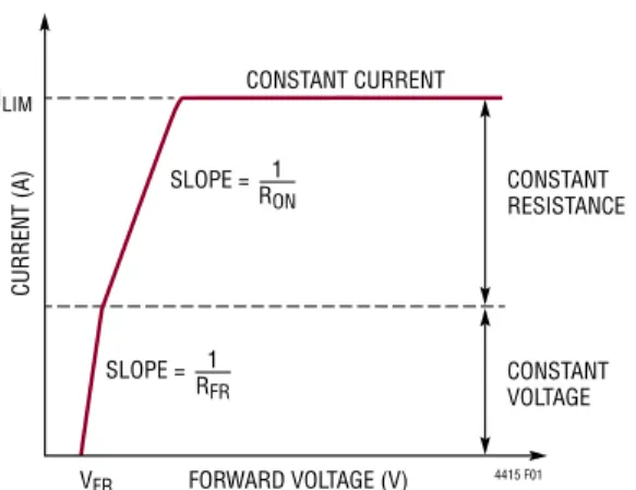
Forward conduction of the LTC4415 diodes has three op-erating ranges as a function of the load current, as shown in Figure 1 and described below:
1. For small load current, a low forward voltage drop (VFR = 15mV typical) is maintained by modulating the series resistance offered by the PFETs (P1/P2) in the current paths as shown in the Block Diagram. This op-erating mode is referred to as constant VFR regulation. In battery-powered and low headroom applications, the low forward drop of the ideal diodes extend the operat-ing range beyond that of Schottky diodes.
2. At higher load currents, the LTC4415 gate driver can no longer modulate the series resistance of the PFETs (P1/P2) to maintain constant forward drop. This transi-tion occurs when the gate voltage of the series PFETs (P1/P2) has been brought down to GND. The ideal diodes subsequently operate with constant resistance, RON, between inputs and outputs, IN1/IN2 and OUT1/ OUT2, respectively.
3. As the load current exceeds the current limit, the series PFETs offer higher resistance between IN1/IN2 and OUT1/OUT2 by reducing the gate drive in order to limit the load current; so the forward voltage drop increases rapidly. This operating mode is referred to as constant current operation.
When the output of either diode is driven higher than its input by an alternate supply, conduction through that diode is suspended to prevent reverse conduction from OUT1/ OUT2 to IN1/IN2. This function allows implementation of a power supply OR function by simply tying the outputs OUT1 and OUT2 together.
Current Limit Setting
The output current limit of each diode can be set inde-pendently by connecting resistors from the current limit adjust pins CLIM1 and CLIM2 to ground. The current out of the CLIM1 and CLIM2 pins are 1/1000 of the ideal diode output currents IOUT1 and IOUT2 respectively. When the load currents increase so that the CLIM1 or CLIM2 pin voltages exceeds 0.5V, the LTC4415 detects an overcurrent condition and regulates the current to a fixed value. The required value of resistor RCLIM for output current limit of ILIM is calculated as follows:
RCLIM=1000 •0.5V ILIM
The allowed range of RCLIM is 125Ω to 1000Ω unless the CLIM1/CLIM2 pins are shorted to GND, in which case the LTC4415 limits the load current using a fixed internal current limit of 6A.
Overcurrent Status
When either of the ideal diodes is operating in current limit, the corresponding warning pin, WARN1/WARN2, is pulled low by an open-drain NFET after a 500µs delay. Normal operation resumes and the warning pin is released
CONSTANT CURRENT CONSTANT RESISTANCE CONSTANT VOLTAGE FORWARD VOLTAGE (V) VFR 4415 F01 CURRENT (A) ILIM SLOPE = 1R ON SLOPE = 1R FR
LTC4415
10
4415fa
when the load current decreases below the current limit. Power consumption in LTC4415 increases during opera-tion in current limit due to the large voltage drop across the PFET devices (P1 or P2).
Load Current Monitor
The current limit pins output 1/1000th of the ideal diode output current. The voltage across the current limit resis-tor can be measured to moniresis-tor the current through each ideal diode as follows:
IOUT=1000 •VCLIM
RCLIM
Note that the current monitor function via VCLIM is not available when CLIM pins are grounded to use the fixed internal current limit.
Soft-Start
An internal soft-start is included for each ideal diode to minimize the start-up inrush current. When either of the diodes start forward conduction, the load current ramps from zero to the set current limit over a period of 2ms. The soft-start can be monitored by observing the CLIM1 and CLIM2 pin voltages when they are connected to grounded resistors. Soft-start duration is reduced to 0.5ms (typical) when the CLIM pins are grounded. In order to minimize output droop during switchover between input sources in power supply ORing applications, soft-start is disabled when the output voltage is above 1.2V.
Forward Conduction Status Monitor
Active low open-drain output status signals, STAT1 and
STAT2, indicate the forward conduction status of each ideal diode. With resistor pull-ups on these status pins, a low voltage indicates forward conduction from input to output, IN1/IN2 to OUT1/OUT2, respectively. The status pins go to high impedance when the respective ideal diodes are disabled, during reverse turn-off conditions, or during thermal shutdown.
Thermal Warning and Shutdown
Thermal sensors within the LTC4415 monitor the die tem-perature when either of the diodes are enabled. When the
die temperature exceeds the warning threshold (130°C), the WARN1/WARN2 pins are pulled down with open-drain NFETs while the LTC4415 continues to operate normally. This gives some time for the user to reduce the load current to avoid thermal shutdown. The warning signal is deas-serted when the die temperature cools down below 115°C. Thermal shutdown is triggered when the internal die temperature increases beyond the fault threshold (160°C). Status pins, STAT1/STAT2, are deasserted during thermal shutdown to indicate the interruption in forward condi-tion. Normal operation resumes when the die temperature cools below 140°C. Note that prolonged operation at the overtemperature condition degrades device reliability. Figure 2 shows WARN followed by thermal shutdown caused by an output short-circuit to ground. Time to thermal shutdown varies depending on power dissipation, ambient temperature and board layout. The output cur-rent ramps up after the device cools down below 140°C, but shuts down repeatedly as the device overheats due to persistent short.
operaTion
Figure 2. Current Limit Warning and Thermal Shutdown on Output Short Circuit
VOUT 2V/DIV IOUT 2A/DIV 10ms/DIV 4415 F02 VIN = 3.6V RCLIM = 124Ω COUT = 4.7µF STAT 5V/DIV WARN 5V/DIV OUTPUT SHORTED TO GND RESTART DUE TO THERMAL HYSTERESIS THERMAL SHUTDOWN
The thermal sensors are independent for each diode to warn of, or shut down the heat generating path so that it does not hinder the normal operation of the other path. Depending on the amount of heat generated, the whole die may still heat up and eventually shut down the other channel.
LTC4415
11
4415faapplicaTions inForMaTion
operaTion
Stability ConsiderationsAny capacitance on the CLIM pins adds a pole to the cur-rent control loop. Therefore, stray capacitance on these pins must be kept to a minimum. Although the maximum allowed value of the current limit adjust resistor is 1000Ω, any additional capacitance on these pins reduces the maximum allowed resistance, consequently increasing the minimum allowed current limit. For stable operation, the pole frequency at the CLIM pins should be kept above 800kHz. Therefore, if the CLIM pin parasitic capacitance is CP, the following equation should be used to calculate the maximum allowed resistor RCLIM:
RCLIM≤ 1
2π•800kHz •CP
When the voltage at the CLIM pins are monitored using a long cable, such as an oscilloscope probe, decouple the parasitic capacitance of the probe and the monitor system using a series resistor as shown in Figure 3, where a 20k resistor has been added between the CLIM pin and the probe to ensure stable operation.
Input and Output Capacitors
High current transients through parasitic inductance on the input and output sides of the ideal diodes can cause volt-age spikes on the IN1/IN2/OUT1/OUT2 pins. These current transients can occur on power plug-in, load disconnect
or switching, disable, or even thermal shutdown. Limit inductance and/or increase bypass capacitors to prevent pin voltages from exceeding the absolute maximum rat-ing of 6V. Some ESR in these capacitors may be helpful in dampening the resonances and minimizing the ringing caused by hot plugging or load switching. Refer to Ap-plication Note 88, entitled, “Ceramic Input Capacitors Can Cause Overvoltage Transients” for a detailed discussion and mitigation of this phenomenon.
The values of the input and output decoupling capacitors also depends on the maximum allowable droop during switchover in power supply ORing applications. Typical du-ration for LTC4415 ideal diodes to switchover from reverse turn-off to forward conduction, tSWITCH, is 9µs. Therefore, the minimum decoupling capacitance, C, required for a specified maximum output voltage droop, ∆V, when one of the input voltages drops, can be calculated as follows:
C=ILOAD• tSWITCH
∆V
where ILOAD is the load current at the time of switchover. For example, the required value of output capacitance for a 100mV maximum droop in the output voltage during quick switchover at 1A load would be 100µF. Note that both supplies share the load during switchover, and therefore reduce the droop, when the voltage on the falling supply pin changes slowly.
Figure 3. Current Monitor with High Capacitance Probe/Instrument
Undervoltage Lockout
Each ideal diode contains an independent UVLO control circuit so that one input experiencing undervoltage lockout does not hinder normal operation of the other channel.
The diode conduction path is turned off and the status signal, STAT1/STAT2, is deasserted during an undervolt-age condition. CLIM PIN CP 4415 F03 CMONITOR RCLIM 20k MONITOR
LTC4415
12
4415fa
applicaTions inForMaTion
Board Layout Considerations
When laying out the printed circuit board, the following checklist should be followed to ensure proper operation of the LTC4415:
1. Connect the exposed pad of the package (Pin 17) directly to a large PC board ground to minimize thermal imped-ance. Correctly soldered to a 2500mm2 double-sided 1oz copper board, the DFN package has a thermal resistance (θJA) of approximately 43°C/W. Failure to make good contact between the exposed pad on the backside of the package and an adequately sized ground plane re-sults in much larger thermal resistance, raising the die temperature for given power dissipation. An example layout for double layer board is given in Figure 4. Via holes are used in the board under and near the device to conduct heat away from the device to the bottom layer.
2. The traces to the input supplies, outputs and their decoupling capacitors should be short and wide to minimize the impact of parasitic inductance. Connect the GND side of the capacitors directly to the ground plane of the board. The decoupling capacitors provide the transient current to the internal power MOSFETs and their drivers.
3. Minimize the parasitic capacitance on CLIM1 and CLIM2 pins for stable operation.
Figure 4. Example Board Layout for a Double-Sided PCB
EN1 IN1 IN2 OUT1 OUT2 4415 F04 CLIM1 CLIM2 WARN1 WARN2 STAT1 STAT2 EN2
LTC4415
13
4415fa
Typical applicaTions
Precision enable inputs and independent status outputs provide flexibility in power supply back up and load share applications using the two high current ideal diode circuits in the LTC4415, as shown in the following examples. The features shown in these application circuits can be com-bined in custom applications as needed.
Prioritized Switchover to a Backup Battery
The application circuit, Figure 5, illustrates switchover from a primary power source to backup power at a pre-cise input voltage using the prioritized power supply-OR application circuit. Diode 2 is enabled when the primary power source voltage on diode 1 input falls below the threshold given as follows:
VIN1<0.8V • 1+R1+R2
R3
As VIN1 falls further, diode 1 is disabled when the primary power source voltage falls below the threshold determined by the resistor divider on enable pin EN1:
VIN1<
(
0.8V – VENHYST)
• 1+ R1R2+R3
The built-in hysteresis on the enable pins in the LTC4415 provides some overlap of diode enables around the swi-tchover of power supplies. Resistor R2 can be optionally used for additional overlap between the two supplies. The additional overlap is given by:
VOVERLAP≈VENTH•R2 R3 when
R2
R3 <<1
The enable overlap minimizes the load voltage droop during switchover. Both input power supplies provide power to the load during the overlap. The status output pins can be pulled up to the output voltage or to a logic power supply.
Automatic Switchover to a Backup Battery and Keep-Alive Power Source
Figure 6 illustrates an application circuit for automatic switchover to the backup battery if the primary power source voltage falls below the backup battery voltage. The wired-AND of the status outputs is used to drive the gate of a pair of back-to-back connected external NMOS (M1 and M2) when both primary and backup power sources are absent or below UVLO or during thermal shutdown of LTC4415. Under these conditions, the keep-alive source supplies power to critical components of the system. At the same time, the wired-AND status output turns off
Figure 5. Prioritized Power Supply ORing
Figure 6. Automatic Switchover to a Backup Battery with Provision for Keep-Alive Power to the Load When Both Are Absent
IDEAL IDEAL LTC4415 GND EN1 R147k 4415 F06 47µF LOAD DMN2215UDM M1 M2 M3 OPTIONAL KEEP ALIVE/ COIN CELL CLIM1 CLIM2 STAT1 WARN1 WARN2 STAT2 EN2 IN2 BACKUP BAT IN1 OUT1 OUT2 PRIMARY POWER SOURCE + IDEAL IDEAL LTC4415 GND EN1 4415 F05 4.7µF TO LOAD R1 R2 R3 RCLIM2 470k RCLIM1 CLIM1 CLIM2 STAT1 WARN1 WARN2 STAT2 EN2 IN2 IN1 OUT1 OUT2 PRIMARY POWER SOURCE SECONDAY POWER SOURCE (BAT) + 470k 470k 470k
LTC4415
14
4415fa
Typical applicaTions
non-critical high current loads. If the status resistors are pulled up through the keep-alive power source itself as shown in Figure 6, the output voltage is limited to: VOUT = VKEEP_ALIVE – Vgs(M1,2)
where Vgs(M1,2) is the voltage drop from gate to source of the composite NMOS device (M1 and M2). The pull-up resistor, R1, consumes power from the keep-alive source when the primary or backup sources supply power to the load. The primary power source or backup battery supplies power to the load when either of them are higher than the output voltage.
Current limit on any of the diode power paths can be set to automatically fold back as the output voltage drops (to reduce power consumption), by switching out a resistor on the CLIM pin, as shown in Figure 6 for diode 1. The gate of NMOS M3 can optionally be fed from a resistor divided output voltage to adjust the output voltage threshold of current foldback.
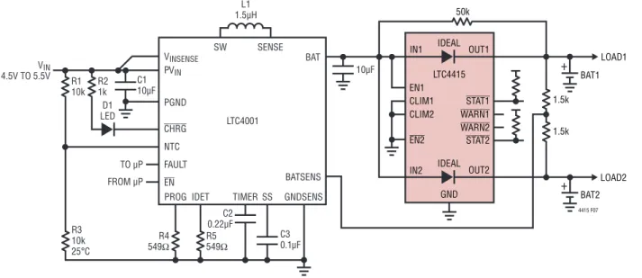
Multiple Battery Charging
Figure 7 illustrates an application circuit for automatic dual battery charging from a single charger. The battery with lower voltage receives larger charging current until both battery voltages are equal, then both are charged. While both batteries are charging simultaneously, the higher capacity battery gets proportionally higher current from the charger. For Li-Ion batteries, both batteries achieve the charger float voltage minus the forward regulation voltage of 15mV. This concept can be extended to more than two batteries using additional LTC4415. The STAT1,
STAT2 pins provide information as to when the batteries are being charged. For intelligent control, the EN1/EN2
input pins can be used with a microcontroller as shown in Figure 9 later in this section.
Figure 7. Dual Battery Charging from a Single Charger
PROG EN FAULT BATSENS TO µP FROM µP NTC CHRG PGND 10µF PVIN VINSENSE BAT IDET TIMER R4 549Ω R5549Ω C2 0.22µF C1 10µF VIN 4.5V TO 5.5V C3 0.1µF SS SW SENSE LTC4001 L1 1.5µH GNDSENS R3 10k 25°C R2 1k D1 LED R1 10k IDEAL 50k IDEAL LTC4415 GND EN1 4415 F07 CLIM1 CLIM2 STAT1 WARN1 WARN2 STAT2 EN2 IN2 IN1 OUT1 OUT2 BAT2 LOAD2 1.5k 1.5k + BAT1 + LOAD1
LTC4415
15
4415fa
Typical applicaTions
Load Sharing by Multiple Batteries and Automatic Switchover to a Preferred Power Supply
(Such as a Wall Adapter)
An application circuit for dual battery load sharing with automatic switchover to a wall adapter (when present) is shown in Figure 8. In the absence of the wall adapter, the higher voltage battery provides the load current until it has discharged to the voltage of the other battery. The load is then shared between the two batteries according to their capacities, the higher capacity battery providing proportionally higher current to the load unless limited by its current limit.
When a wall adapter is applied, the output voltage rises as the body diode of PFET MP1 conducts and both of the ideal diode paths in the LTC4415 stop conducting due to reverse turn-off. At this time, the wired-OR status signal pulls up the gate voltage of NFET MN1, pulling down the gate voltage of power PFET MP1, turning it on. The wired-OR status signal indicates whether the wall adapter or either of the two batteries is supplying the load current. The two application circuits described in Figure 7 and Figure 8 can be cascaded for dual battery charging and load sharing.
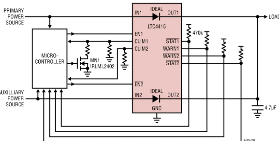
Microcontrolled Power Switch with Reverse Blocking, Selectable Current Limit, Soft-Start and Monitoring
Figure 9 illustrates an application circuit for microcon-troller monitoring and control of two power sources. The microcontroller monitors the input supply voltages and commands the LTC4415 through EN1/EN2 inputs. Currents through the ideal diodes are monitored by the microcontroller measuring CLIM1/CLIM2 pin voltages using ADCs. The current limit can be adjusted for either diode using an external FET as shown in this application for diode 1 with MN1. The two ideal diode outputs are connected together for power source ORing, or they may feed different loads.
Parallel Diodes for Lower Resistance or Higher Current Output
The two ideal diodes in the LTC4415 can be connected in parallel as shown in Figure 10 to achieve a low resistance PowerPath. The master enable input, ENABLE, turns on diode 2. EN1 is tied to the output so that diode 1 conducts only after the output has charged up (by diode 2 according to its current limit setting). Diode 1 is disabled when the
Figure 8. Dual Battery Load Sharing with Automatic Switchover to a Wall Adapter
IDEAL IDEAL LTC4415 GND EN1 470k MN1 IRLML2402 CLIM1 CLIM2 STAT1 STAT WARN1 WARN2 STAT2 EN2 IN2 BAT2 BAT1 IN1 OUT1 OUT2 470k 4.7µF + MP1 IRFHS9301 WALL ADAPTER PVIN1 PVIN2 SW2 SW3 FB2 FB3 VOUT1 LTC3521 SHDN2 SHDN1 1.0M 137k 68.1k 10µF VIN 4.7µH 4.7µH VOUT1 3.3V 0.8A VOUT2 1.8V 0.6A 100k 100k 10µF 4.7µH VOUT3 1.2V 0.6A 221k 4415 F08 SHDN3 PWM SW1A SW1B FB1 PGOOD2 PGOOD1 PGOOD3 PGND1A PGND2 GND PGND1B ON OFF PWM BURST +
LTC4415
16
4415fa
Figure 10. Parallel Diodes with Current Limit Foldback and Reverse Polarity Protection
output falls below a threshold set by the resistor divider on EN1 pin. This arrangement results in current limit foldback, reducing the current limit of the parallel diodes to that of only diode 2 when the output voltage falls, thus controlling power dissipation.
An optional Schottky diode can be inserted in series with the chip ground as shown in Figure 10 to protect LTC4415 against input power source reverse polarity. The presence of the Schottky shifts the UVLO and enable pin thresholds by a voltage equal to the forward voltage drop of the Schottky diode.
Power Backup Using Supercapacitors and Optional Keep-Alive Cell
An application of dual backup power is shown on the last page of this data sheet. Diode 2 provides power to the triple DC/DC converter (LTC3521) when the primary input
power (VDD) is available, possibly from a wall adapter. When the input power falls below the supercapacitor voltage, the supercapcitor provides power to the LTC3521. The supercapacitor charger (LTC3625) provides a power failure comparator output signal (PFO) when its input voltage falls below a preset voltage defined by the resistive divider on the PFI input. The PFO signal is available to start the shutdown of high current applications. When the super-capacitor discharges to a voltage level determined by the resistor divider on EN1 input of LTC4415, the wired-AND status signal of LTC4415 pulls up because neither of the diode paths in LTC4415 are conducting and the coin cell provides power through a back-to-back connected pair of NFETs, M1 and M2. The wired-AND status signal is available to signal that only low current circuits such as real-time clock or memory remain enabled while operating from the coin cell.
Figure 9. Microcontrolled PowerPath Monitoring and Control
Typical applicaTions
IDEAL IDEAL LTC4415 GND EN1 MN1 IRLML2402 470k 4415 F09 4.7µF LOAD CLIM1 CLIM2 STAT1 WARN1 WARN2 STAT2 EN2 IN2 IN1 OUT1 OUT2 PRIMARY POWER SOURCE AUXILLIARY POWER SOURCE MICRO-CONTROLLER IDEAL IDEAL LTC4415 GND EN1 470k 4415 F10 LOAD CLIM1 CLIM2 STAT1 WARN1 WARN2 STAT2 EN2 IN2 D1 1N5817 IN1 OUT1 OUT2 POWER SOURCE ENABLELTC4415
17
4415fa 3.00 ±0.10 (2 SIDES) 5.00 ±0.10 (2 SIDES) NOTE:1. DRAWING PROPOSED TO BE MADE VARIATION OF VERSION (WJED-1) IN JEDEC PACKAGE OUTLINE MO-229
2. DRAWING NOT TO SCALE
3. ALL DIMENSIONS ARE IN MILLIMETERS
4. DIMENSIONS OF EXPOSED PAD ON BOTTOM OF PACKAGE DO NOT INCLUDE MOLD FLASH. MOLD FLASH, IF PRESENT, SHALL NOT EXCEED 0.15mm ON ANY SIDE 5. EXPOSED PAD SHALL BE SOLDER PLATED
6. SHADED AREA IS ONLY A REFERENCE FOR PIN 1 LOCATION ON THE TOP AND BOTTOM OF PACKAGE
0.40 ±0.10
1.29 REF
BOTTOM VIEW—EXPOSED PAD 1.65 ±0.10 (2 SIDES) 0.75 ±0.05 R = 0.115 TYP R = 0.20 TYP 4.40 ±0.10 (2 SIDES) 1 8 16 9 PIN 1 TOP MARK (SEE NOTE 6) 0.200 REF 0.00 – 0.05 (DHC16 Var A) DFN 0410 0.25 ±0.05 PIN 1 NOTCH 0.50 BSC 4.40 ±0.05 (2 SIDES)
RECOMMENDED SOLDER PAD PITCH AND DIMENSIONS
1.65 ±0.05 (2 SIDES) 2.20 ±0.05 0.50 BSC 0.65 ±0.05 1.29 ±0.05 3.50 ±0.05 PACKAGE OUTLINE 0.25 ± 0.05 DHC Package 16-Lead Plastic DFN (5mm × 3mm) (Reference LTC DWG # 05-08-1872 Rev Ø) Variation A
package DescripTion
LTC4415
18
4415fa
package DescripTion
Please refer to http://www.linear.com/designtools/packaging/ for the most recent package drawings.
MSOP (MSE16) 0911 REV E
0.53 ±0.152 (.021 ±.006) SEATING PLANE 0.18 (.007) 1.10 (.043) MAX 0.17 – 0.27 (.007 – .011) TYP 0.86 (.034) REF 0.50 (.0197) BSC 16 16151413121110 1 2 3 4 5 6 7 8 9 9 1 8 NOTE: 1. DIMENSIONS IN MILLIMETER/(INCH) 2. DRAWING NOT TO SCALE
3. DIMENSION DOES NOT INCLUDE MOLD FLASH, PROTRUSIONS OR GATE BURRS.
MOLD FLASH, PROTRUSIONS OR GATE BURRS SHALL NOT EXCEED 0.152mm (.006") PER SIDE 4. DIMENSION DOES NOT INCLUDE INTERLEAD FLASH OR PROTRUSIONS.
INTERLEAD FLASH OR PROTRUSIONS SHALL NOT EXCEED 0.152mm (.006") PER SIDE 5. LEAD COPLANARITY (BOTTOM OF LEADS AFTER FORMING) SHALL BE 0.102mm (.004") MAX 6. EXPOSED PAD DIMENSION DOES INCLUDE MOLD FLASH. MOLD FLASH ON E-PAD SHALL NOT EXCEED 0.254mm (.010") PER SIDE.
0.254 (.010) 0° – 6° TYP DETAIL “A” DETAIL “A” GAUGE PLANE 5.23 (.206) MIN 3.20 – 3.45 (.126 – .136) 0.889 ±0.127 (.035 ±.005)
RECOMMENDED SOLDER PAD LAYOUT 0.305 ±0.038 (.0120 ±.0015) TYP 0.50 (.0197) BSC BOTTOM VIEW OF EXPOSED PAD OPTION
2.845 ±0.102 (.112 ±.004) 2.845 ±0.102 (.112 ±.004) 4.039 ±0.102 (.159 ±.004) (NOTE 3) 1.651 ±0.102 (.065 ±.004) 1.651 ±0.102 (.065 ±.004) 0.1016 ±0.0508 (.004 ±.002) 3.00 ±0.102 (.118 ±.004) (NOTE 4) 0.280 ±0.076 (.011 ±.003) REF 4.90 ±0.152 (.193 ±.006) DETAIL “B” DETAIL “B” CORNER TAIL IS PART OF THE LEADFRAME FEATURE.
FOR REFERENCE ONLY
NO MEASUREMENT PURPOSE
0.12 REF 0.35 REF
MSE Package
16-Lead Plastic MSOP, Exposed Die Pad
LTC4415
19
4415fa Information furnished by Linear Technology Corporation is believed to be accurate and reliable.
However, no responsibility is assumed for its use. Linear Technology Corporation makes no representa-tion that the interconnecrepresenta-tion of its circuits as described herein will not infringe on existing patent rights.
revision hisTory
REV DATE DESCRIPTION PAGE NUMBER
A 4/12 Clarified footnotes and added new Note 5 for quiescent current Changed FET MP1 part number on Figure 8
3, 4 15
LTC4415
20
4415fa
Linear Technology Corporation
1630 McCarthy Blvd., Milpitas, CA 95035-7417
(408) 432-1900 ● FAX: (408) 434-0507 ● www.linear.com LINEAR TECHNOLOGY CORPORATION 2011
LT 0412 REV A • PRINTED IN USA
relaTeD parTs
Typical applicaTion
Power Backup Using Supercapacitors and Optional Keep-Alive Cell
PART NUMBER DESCRIPTION COMMENTS
LTC4411 2.6A Low Loss Ideal Diode Monolithic Low Loss PowerPath, ThinSOT Package
LTC4412 PowerPath Controller 3V to 28V Input Voltage Range, ThinSOT Package
LTC4413-1/
LTC4413-2 Dual 2.6A, 2.5V to 5.5V, Ideal Diodes in 3mm × 3mm DFN 140mΩ On-Resistance, Overvoltage Protection Sensor with Drive Output LTC4414 36V, Low Loss PowerPath Controller for Large PFETs Drives Large QG PFETs, 3.5V to 36V
LTC4416 36V, Low Loss Dual PowerPath Controllers Designed to Drive Large and Small QG PFETs, 3.5V to 36V
LTC4352 Low Voltage Ideal Diode Controller With Monitoring Controls Single N-Channel MOSFET, Input Supply Monitors, 2.9V to 18V LTC4354 Negative High Voltage Diode-OR Controller and Monitor Controls Two N-Channel MOSFETs, 4.5V to 80V
LTC4355 Positive High Voltage Diode-OR Controller and Monitor Controls Two N-Channel MOSFETs, 9V to 80V LTC4357 Positive High Voltage Ideal Diode Controller Controls Single N-Channel MOSFET, 9V to 80V
LTC4358 5A Monolithic Ideal Diode 20mΩ N-Channel MOSFET, 9V to 26.5V
LTC4066 USB Power Controller and Li-Ion Linear Charger with Low
Loss Ideal Diode Seamless Transition Between Input Power Sources: Li-Ion Battery, USB and 5V Wall Adapter LTC4425 Linear Supercapacitor Charger with Current-Limited Ideal
Diode and V/I Monitor 50mΩ On-Resistance, 2.7V to 5.5V, Programmable Current Limit, Programmable Output Voltage Mode LTC2952 Pushbutton Ideal Diode PowerPath Controller with
Supervisor Controls Two P-Channel MOSFETs, 2.7V to 28V
IDEAL IDEAL LTC4415 GND EN1 M2 CLIM1 CLIM2 STAT1 WARN1 WARN2 STAT2 EN2 IN2 IN1 OUT1 OUT2 125Ω 300k 200k 125Ω M1 PVIN1 PVIN2 SW2 SW3 FB2 FB3 VOUT1 LTC3521 SHDN2 SHDN1 1.0M 137k 68.1k 10µF VIN 4.7µH 47k 4.7µH L1 3.3µH VDD 294k 100k RPROG 78.7k L2 3.3µH VOUT1 3.3V 1A KEEP-ALIVE/COIN CELL VOUT2 1.8V 0.6A 100k 100k 10µF 4.7µH VOUT3 1.2V 0.6A 221k 4415 TA02 SHDN3 PWM SW1A SW1B FB1 PGOOD2 PGOOD1 PGOOD3 PGND1A PGND2 GND PGND1B ON OFF PWM BURST 47µF DMN2215UDM 22µF CTOP 360F CBOT 360F SW1 VOUT SW2 EN VIN PFI VSEL CTL GND GND VMID PFO PROG LTC3625