IJEDR1703147
International Journal of Engineering Development and Research (
www.ijedr.org
)
1043
Implementation of Scan Insertion and Compression
for 28nm design Technology
1Mohan PVS, 2Rajanna K.M
1PG Student, Department of ECE, Dr. Ambedkar Institute of Technology, Bengaluru, India
2Associate Professor and HOD, Department of ECE, Dr. Ambedkar Institute of Technology, Bengaluru, India
________________________________________________________________________________________________________
Abstract —Scan Insertion and Scan Compression are necessary for design-for-testability (DFT) methodology, which helps
to achieve very high quality testability feature for the design at low costs. Scan Insertion methodology is improving over the years and the Scan Compression is improving and meeting the needs by providing the testability feature for the designs. In this paper, the implementation of the Scan Insertion and Compression techniques in the 28nm technology is been presented. We implemented Scan Insertion and compression technology and also, we discuss about the clock and reset DRCs and how the compression help in testing the integrated circuit by reducing the test time and test data volume. ________________________________________________________________________________________________________
I. INTRODUCTION
The development in technology scaling will results in increase in power density and heat dissipation due to switching operation of the transistors which results in the damages in the IC, reduction in reliability and less yield. Clock gating, voltage shut-off and other methods must be followed when operated in the functional mode. Preventing heat and power issues during the functional operation conflicts with controllability and observability.DFT technique is proposed to provide the controllability and observability feature for the internal nodes in a design, Controllability means able to change the signal value to the required logic from the inputs and observability means able to observe the changed signal line logic value at the outputs. The paper briefs the implementation of the scan insertion and compression to the design and the way to handle the DRC violations. First focus will be on scan flops conversion in the design and checking for the DRC violations, if there are any DRC violations then fixing them using the commands and after fixing the DRCs scan flops stitching has to be done to form the scan chain and after analysing , it is observed that the number of patterns required will be more due to the more number of scan flops in the single chain. Hence the scan compression is performed in order to reduce the pattern length and tester memory usability. After inserting the scan compression logic again the DRCs has to be verified and if any DRCs found need to be fixed and through scan compression the number of the scan flop stitched in the single chain can decided by compression ratio. This scan insertion and compression is been implemented using the synopsis tool design compiler.
II. RELATEDWORK
Heiko Ahrens et al., [1] presented about the implementation and testing of a DFT architecture for a Power PC based microprocessors for various automotive applications which has to result in high quality levels and low test cost. Hence the new architecture consists of dual compression for two different CAD flows but results in overhead of silicon area and engineering resources. So there are two possibilities to overcome this, that is there has to be an agreement between the two companies based on the ATPG and diagnostic tools used, which is very difficult due to financial and technical problems. The second approach is to use the same compression IP by the ATPG and diagnostic tools of the two companies.
A.Chandra et al., [2] proposed industrial view of demonstrating how DFT flows will impact in the presence of compression logic. Hence various DFT architectures are developed using zScan compression technology and discussed pros and cons of each DFT flow with modular DFT insertion. The pin count and scan chain count impact on the QoR(test application time and test data volume requirement). Design teams can use the analysis in this paper to determine DFT strategy for compression. Swapnil Bahl, Shreyans Rungta et al., [3] proposed the different compression schemes DFTMAX. DFTMAX Ultra technology that provides a single solution for all needs. In this paper we discuss the variety of design scenarios from the scan compression point of view. In this paper, they have presented a single compression solution to satisfy the Scan compression requirement for a chip.
Satyendra N. Biswas ,Sunil R. D et al., [4] proposed the way to increase the ATE throughput by vector compression, The compression and decompression algorithm must be simple such that there should not be any pattern loss and should not consume more time to reduce the overall processing time of the ATE. The compression method is based on a hybrid technique which targets on the unique characteristics of the block matching test data compression, BWT along with several coding algorithms reduces the number of transitions for the test vector sequences and results in a high compression ratio in the first stage of the proposed technique.
IJEDR1703147
International Journal of Engineering Development and Research (
www.ijedr.org
)
1044
III. DFTFLOWFORSCANINSERTIONANDCOMPRESSION
First invoke the tool using dc_shell(design compiler) and netlist should be read, the netlist will be in Verilog(.v) or Syste m Verilog(.vs) format using read_file command and set the top module as a current design using the command set current_design. By using the link command, the netlist can be linked with the libraries , the normal flip-flops are converted into scan flip-flop by using the compile -scan command and by defining the configuration type as multiplexed_flip_flop. The clocks ,reset and enable singles are defined using set_dft_signal command, create the scan input and scan output port for all the scan chains using create_port command and define the type of the port (scandatain or scandataout) using -type option in the set_dft_signal command. Define the scan chain path for stitching with the help of set_scan_path command, to create the test default port make use of create_test_protocol command and then check the DRC violations using dft_drc and then fix the respective DRCs and the scan stitching is done.
Then the scan stitching is done using the insert_dft command, the DRC checking is done and DRCs are fixed using the set_auto fix_configuration command and the scan inserted netlist ,reports,.ctl files can be generated using write_test_protocol command.
IV. SCANCOMPRESSION
The scan compression logic reduces the test time and tester memory without loss in the test coverage. The components of the scan compression logic are decompressor and compactor and they are part of scan path, hence functional timing is not affected. Compression logic can be at the design top level or can be placed inside each core of the design. It provides the highest coverage for the design and efficient use of tester pins.
pins, called load-modepins, are dedicated to the MUX select signals.
In the decompressor logic structure every scan cell must be uniquely controllable in every pattern. Only a sparse set of scan cells are required to be controlled in a pattern. As the scan channels increases, in order to provide controllability the number of scan chain increases.
IJEDR1703147
International Journal of Engineering Development and Research (
www.ijedr.org
)
1045
Fig. 2 Decompressor Operation
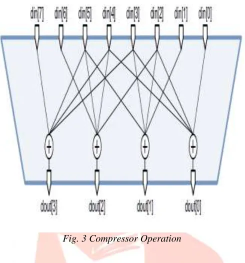
The compressor outputs drives combinations of compressed scan chains, combined using XOR logic. An fault from a compressed scan chain results in a specific incorrect values at the compressor outputs.
The compressor input are the scan chains. As the compressed scan chain count increases, more XOR configurations are needed. If the chain count is increased, the XOR configurations must repeat, which can impact the diagnosability of the design. As the compressor output channel width increases, the number of fault observed at output port decreases. Thus diagnosability of the design improves, especially when multiple faults diagnosed simultaneously.
Fig. 3 Compressor Operation
V. RESULTS
Synopsis tool (Design compiler) is used for is used for scan insertion and compression for an 28nm technology. The normal flip-flop conversion into the multiplexed scan flip-flip-flop and scan flip-flip-flop stitching is as shown in the Figure.4 and the chain length depends on the number of scan flip-flops in the design.
IJEDR1703147
International Journal of Engineering Development and Research (
www.ijedr.org
)
1046
Fig. 4 Scan Stitching
The scan chain information after the scan flow execution is shown in Figure.5
IJEDR1703147
International Journal of Engineering Development and Research (
www.ijedr.org
)
1047
Fig. 6 DRC Report
Two DRC violations observed during scan insertion, one is the clock violation and the other is the reset violation. The clock has to be driven from the port pin, if the clock to a scan flip-flop is driven from any other combinational logic or from data path then the clock violation occurs. Figure.7 shows the clock violation which occurred due to the clock port of the scan flip-flop is driven from the Q output of the other scan flip-flop. Not all flip-flops in the design converts in to the scan flops, for example the flip flops of the shift register in the on chip clock (occ) circuitry.
Fig. 7 Clock DRC Violation
IJEDR1703147
International Journal of Engineering Development and Research (
www.ijedr.org
)
1048
Fig. 8 RESET DRC Violation
In this the reset pin is not controlled from the port level,the reset signal to the flip-flop is coming from the AND gate, hence the controllability of the reset signal is difficult. Thus these DRC s can be fixed using the command set_autofix_configuration command.
For large design without scan compression the pattern length will be more hence more number of shifting cycles required will be more and the tester time and memory will also increase thus in order reduce the tester time and tester memory we introduce scan compression logic in the design.
Scan Compression logic consists of decompressor and comparator logic. The decompressor logic consists of the LFSR(linear shift feedback register) along with the phase shift flip-flops. The decompressor logic distributes the compressed patterns from the input channels to the scan chains. The decompressor logic implemented for the design is as shown in the Figure.9. The number of input channels and scan chains depend on the compression ratio.
Fig. 9 Decompressor Logic
IJEDR1703147
International Journal of Engineering Development and Research (
www.ijedr.org
)
1049
Fig. 10 Compactor Logic
VI. CONCLUSIONS
Aim is to implement the DFT methodology to the 28nm design technology by scan inserting and stitching and by introducing the compressor logic which makes the 28nm design technology testable. Thus, by using the Scan Compression we can reduce the tester time to test the integrated circuit. But as the tool version changes the scan compression logic changes that is new logics are included which simplifies the scan compression. Hence scan insertion and compression DFT steps is implemented on top module which is of 28nm design technology. With better tools the DFT steps can be applied to the further technologies with better coverage. Since the MBIST (Memory Built In Self Test) circuitry consists of flip-flops , so first step in DFT flow is to insert and verify the BIST and boundary scan circuitry and then continue with the scan insertion and compression flow.
VII. REFERENCES
[1] Heiko Ahrens, Rolf Schlagenhaft, Helmut Lang, V. Srinivasan, Enrico Bruzzano, “DFT Architecture for Automotive Microprocessors using On-Chip Scan Compression supporting Dual Vendor ATPG”, 2008
.[2] A. Chandra, S. Chebiyam, and R. Kapur ,”A Case Study on Implementing Compressed DFT Architecture”, 2014.
[3] Swapnil Bahl, Shreyans Rungta, Shray Khullar, Rohit Kapur, Anshuman Chandra, Salvatore Talluto, Pramod Notiyath, Ajay Rajagopalan, “Unifying Scan Compression”, 2014.
[4] Satyendra N. Biswas ,Sunil R. Das ,Emil M. Petriu, “On System-on-Chip Testing Using Hybrid Test Vector Compression”, 11, NOVEMBER 2014.
[5] Prakash Srinivasan, Ronan Farrell, “Hierarchical DFT with Combinational Scan Compression, Partition Chain and RPCT”, 2010.
[6] Y. Zorian, E. J. Marinissen, and S. Dey, “Testing embedded-corebasedsystem chips,” Computer, pp. 52–60, June, 1999. [7] E. J. Marinissen, R. Kapur and Y. Zorian, “On using IEEE P1500SECT for test plug-n-play,” Proc. Int. Test Conf., pp.770–
777,2000.
[8] E. Larsson and Z. Peng, “Test sch. and scan-chain division underpower constraint,” Proc. Asian Test Symp., pp. 259–264, 2001.
[9] K. Chakrabarty, V. Iyengar and M. D. Krasniewski, “Test planningfor modular testing of hierarchical SoC”, Trans. CAD of Integrated Circuits and Systems, vol. 24, pp. 435–447, March 2005.
[10] Q. Xu and Ni.Nicolici, “Time/Area tradeoffs in testing hier.SoC with hard mega core”, Proc. Int. Test Conf., pp.1196–1202, 2004.
[11] V. Iyengar, K. Chakrabarty and E. J. Marinissen, “Test access mechanism opt., test sch. and tester data volume reduction for system-on-chip,” Trans. on Computers, pp. 1619–1632, Dec. 2003.
[12] B. Nadeau-Dostie, Saman M.I. Adham and R. Abbott, “Improved Core Isolation and Access for Hierarchical Embedded Test”, IEEE Design and Test of Comp., Vol. 26, pp.18–25, Feb. 2009.