IJSRST16211 | Received: 04 Jan-2017 | Accepted : 19 Jan-2017 | January-February-2017 [(3)1: 95-102 ]
© 2017 IJSRST | Volume 3 | Issue 1 | Print ISSN: 2395-6011 | Online ISSN: 2395-602X Themed Section: Science and Technology
95
Growth Mechanism and Influence of Annealing Temperature on
Structural and Compositional Properties of Cu
2ZnSnS
4(CZTS) thin
Films Deposited by RF Sputtering Method from a Compound Target
S. Abdullahi*1, M. Momoh1, A. U. Moreh1, A. M. Bayawa2, B. Hamza1, G. M. Argungu1, O. T. Popoola3
*1Department of Physics Usmanu Danfodiyo University Sokoto, Nigeria
2Department of Pure and Applied Chemistry Usmanu Danfodiyo University Sokoto, Nigeria 3Department of Mechanical Engineering Florida International University Miami, Florida, U.S.A
ABSTRACT
Kesterite-type Cu2ZnSnS4 (CZTS) thin films were deposited on corning glass from a single quaternary target. In this
study, we report the growth mechanism and the influence of annealing temperature on the structural and compositional properties of CZTS films. All the four samples (as-deposited inclusive) show peaks corresponding to kesterite-type structure. The diffraction peaks of (112) are sharp and the small characteristics peaks of the kesterite structure such as (220)/ (204) and (312)/ (116) are also clearly observed in X-ray diffraction pattern. Some secondary phases that appeared as a result of the annealing were observed in the Raman spectra. These results indicate that the quaternary CZTS would be a potential candidate for solar cell applications.
Keywords: RF Sputtering, Cu2ZnSnS4 thin Film, Annealing, Growth Mechanism, Renewable Energy.
I.
INTRODUCTION
CZTS is a p-type semiconductor, and as a photovoltaic device it has a theoretical efficiency limit of 30% ([1-2]. Thus, it is a very viable material for the future of optoelectronic industry. It is a quaternary chalcogenide typically produced in Kesterite phase. It has a band gap of 1.0-1.5 eV, and large absorption coefficient in the range of 104 cm-1, thus a very thin layer of film (0.45-2 m) can absorb over 90% of the photons over the spectrum with photon energy higher than the band gap [3]. Advances in the industry have brought its current efficiency up to a maximum of 11% as developed by IBM using a selenium/sulfur substitute to gain efficiency [4]. It is formed entirely from earth abundant, inexpensive, non-toxic elements [5].
CZTS can be synthesized using vacuum, non-vacuum, thin film, and nano crystal production processes. Majority of the synthesis methods involve depositing the CZTS material onto a substrate as a thin film, but it is also possible to produce CZTS nano crystals. A variety of synthesis techniques exist due to the common existence of multiple phases and common compound impurities such as Cu2S, thus these methods all attempt
to find a new way to make phase pure CZTS [6]. These
methods or techniques include thermal and electron-beam evaporation [7] co-evaporation [8], DC and RF magnetron sputtering [9-13], hybrid sputtering [14], spray pyrolysis [15], sol-gel spin-coated deposition, electro deposition (co-electroplating)[16-17], Chemical bath deposition [18], One temperature method [5] and SILAR [19].
II.
METHODS AND MATERIAL
A. Fabrication of CZTS Compound Target
Pressing and sintering are the mechanisms used to form solid parts from powders. Pressing occurs first, then sintering. In addition to the powder constituents, binders, deflocculates, lubricants may also be present in the mixture.
In this work, the preparation of the CZTS single target starts with the mixing of CuS, ZnS and SnS2 (purity: 99.99%; supplier: AJA International) raw powders at a different weight ratios of Cu:Zn:Sn:S = 1.1:1.8:0.9:1.0 with the theoretical stoichiometry of Cu1.1Zn1.8Sn0.8S1.0.
The powders were mixed by using the ball milling method at the rotating speed of 300 rpm for 3 h, poured into a stainless steel mold, pressed into a pellet form with 6 mm in diameter at a pressure of 1.38 , and transferred to a vacuum furnace for hot sintering treatment. The pellet sample was sintered at 6000C for 8 h then taken out from the furnace for the microstructure and phase characterizations in order to identify the sintering conditions that may yield the single-phase CZTS structure. Afterward, the 2-inches 0.125-inch CZTS target was prepared in accord with the optimum sintering conditions. The raw powder was mixed at the weight ratios as delineated above, poured into a 2-inch stainless steel mold, pressed into the 2-inch disc form at the pressure of 1.38 , and transferred into a vacuum furnace for sintering.
With the target at hand, the growth starts with the substrate cleaning. The substrate used in this work is corning glass (microscope slide) having dimensions of 25 mm. Throughout the processing steps, great care was taken in order to ensure the cleanliness of the sample surfaces, as dirt and dust on the substrate prevents the material to be deposited from sufficiently bonding to the surface. The biggest source of contamination on the part of the substrate is the environment in which it is kept or stored.
All depositions described here were carried out in a class100 clean room. Common procedures for substrate cleaning (more especially in dealing with thin film) include an RCA (a procedure developed by Warner
Kern), HO (hydrogen peroxide) – NHOH
(Ammonium hydroxide) – H2O (Water) for removing
organic residue and solvent cleaning with acetone, methanol and IPA to remove remaining contaminates. Before the deposition, the substrates were kept in a dilute chemical detergent (a detergent solution used in the laboratory to solubilize biological macromolecules such as proteins) solution at 100°C in ultrasonic bath for 10 minutes to remove oils and protein molecules and rinsed with double distilled water to remove possible left
detergent contaminants. To remove organic
contaminants, the substrates were boiled in dilute (hydrogen peroxide-H2O2) solution for 15 minutes. The
same solution was put into the ultrasonic bath. The substrates were extracted from the bath and rinsed with distilled water and later dried with 4N Nitrogen gas before being introduced into the sputtering chamber. Throughout the period of substrate preparation, film deposition and film characterization, the laboratory staff wore protective clothing so as not to contaminate the samples.
The deposition begins with loading the target and securing the glass substrate(s) to the substrate holder. The sputtering machine, consists of a stainless steel chamber with a cover that moves vertically (up and down) and three sputter magnetron guns (1 gun can be used at a time) of 2 cm in diameter each located at the bottom of the chamber. The chamber is normally evacuated and then partially filled with nitrogen gas to about 0.13-0.27 Pa so as to keep it clean. The target is a single disk composed of CZTS of 99.99% purity (fabricated through hot sintering by AJA International) having a diameter of about 2 inches and a thickness of about 0.25 cm. A one-minute pre-sputtering has been carried out. Sputtering deposition of CZTS layer using single-phase CZTS target offers the advantages of uniform composition, smooth surface morphology and relatively simple process; however, the composition deviation in between sputtering target and deposited layer is the major difficulty of this method. The thickness of the deposited films is 450nm.
B. Annealing/heating the Samples
and the dwelling time was 1 hour. The samples were annealed under nitrogen gas flowing at 10sccm per minute. The purity of the gas is 99.99%.
C. Structural characterizations
The structural properties of thin films were analysed by high-resolution X-ray diffraction (XRD – SIEMENS Diffractometer D5000) operated at 40 kV and 30 mA and also by Raman scattering spectroscopy (Renishaw invia Raman Microscope) with an Olympus microscope equipped with a 100X magnification lens and in the backscattering configuration. The excitation source was a green Argon ion laser operating at 532 nm and 220 mW output powers. The surface morphology and the elemental analysis of the samples were done with field emission scanning electron microscopy (FE-SEM, Model: JBM-7000F, Japan). The samples are referred to as CZTS1, CZTS2, CZTS3 and CZTS4, with CZTS1 as the as-deposited sample. All the measurements were done at room temperature.
III.
RESULTS AND DISCUSSION
There are many possibilities for the formation of binary sulfides secondary phases because of the presence of four elements in the semiconductor. The appearance of these secondary phases may be due to the inhomogeneous composition-distribution of the sputtering target in local-regions which leads to the existence of small impurity sulfides phases as suggested by [20].
A. XRD analysis.
It is very difficult to distinguish the between kesterite and stannite structure due to the fact that the XRD patterns of these two structures differ only slightly in the splitting of high order peaks, such as (2 2 0)/(2 0 4) and (1 1 6)/(3 1 2) resulting from a slightly different tetragonal distortion (c/2a) [13]. In general, [21] suggested that narrow peaks indicate good crystallinity of the samples.
TABLE 1 Samples Parameters
S/no Name Thickness
(nm)
Annealing Temp (0C)
1 CZTS1 450 None
(as-deposited)
2 CZTS 2 450 250
3 CZTS 3 450 350
4 CZTS 4 450 450
TABLE 2 Deposition Parameters
S/ No.
Parameter Deposition Details
1 Substrate Corning Glass
2 Target CZTS (4N purity)
3. Substrate/Target Distance 7 cm
4. Annealing Environment Nitrogen of 4N purity
5. Annealing set points 250oC, 350oC and 450oC
6. Annealing Ramp rate 10oC/min. 7. Dwelling period 30 minutes 8. Film Thickness (nm) 450
9. Deposition pressure 1333.22 Pa 10. Argon/Oxygen flow rate 20 sccm
11. Substrate temp 100 0C.
12. RF power 75 W.
13. Deposition rate 3nm/min
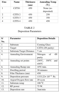
Figures 1a, 1b, 1c and 1d show the XRD patterns of the samples of thickness 450nm (CZTS 1, 2, 3 and 4). Figure 1a is the XRD pattern of the as-deposited sample. It can clearly be seen that the two most prominent broad peaks appeared at 2 = 31.70 and 42.50 which according to JCPDS card no. 00-036-1451 and 01-1010 belongs to ZnO and SnS2 respectively, [22] reported similar results.
In figure 1b, the peaks exhibited are located at 28.50, 42.50 and 47.40 for Kesterite (JCPDS card no 26-0575 CZTS) same results were obtained by [23-26] and (JCPDS card no 01-1010 SnS2) as explained by [20].
Figure 1c is dominated by peaks located at 27.000 and 29.960 which belong to SnS as referenced in JCPDS card no 04-002-9907 while the latter belongs to the secondary phase of Cu2SnS2 with card no 04-010-5719 respectively
is located at 2 = 27.000 classified as SnS. In figure 1d the peak is much more pronounced than in figure 1c. This increase in intensity is not unconnected with the increase in the annealing temperature from 350-4500C.
Figure 1: (a) XRD pattern of CZTS 1(as-deposited) and (b) CZTS 2 (sample annealed at 2500C) (c) XRD pattern of CZTS 3(sample annealed at 3500C) and (d) CZTS 2
(sample annealed at 4500C).
B. Raman analysis
Figures 2abc and d shows the measured Raman spectra for the CZTS1, CZTS2, CZTS3 and CZTS4 samples at room temperature. All the samples excepting the as-deposited (Figure 2a) show a strong peak at 338 cm-1 with additional peaks at 287 cm-1, which is associated with the formation of the CZTS phase. The strongest peak at 337 cm-1 along with the presence of peak at 287 cm-1 is attributed to the A1 symmetry of Kesterite. These
A1 modes are pure anion modes which correspond to the
vibration of sulphur atoms surrounded by motionless neighbouring atoms [1]. The additional peak observed at 310 cm-1 is related to the formation of Sn2S3.
In Figure 2c, a shoulder peak of the main peak at 349 cm-1 and a broad peak at about 368 cm-1 were also observed, which is in agreement with the reported results for CZTS. The shoulder peak at 349 cm-1 and the other peak at 368 cm-1 are attributed to the Transverse optical (TO) modes and Longitudinal Optical (LO) mode of Kesterite CZTS phase respectively. Absence of peak at 277 cm-1 in Figure 2d, which is a characteristic peak of Stannite phase in CZTS indicates that the CZTS phase formed in the annealed sample exhibit dominant Kesterite phase, which is favourable for its application as an absorber in the solar photo voltaic (PV). Thus, the presence of these four peaks i.e. 287 cm-1, 337 cm-1, 349 cm-1 and 368 cm-1 in the Raman spectra of Figures 2b, c and d confirms the formation of Kesterite CZTS phase in the compound. Sharp and strong major peak indicates the good crystalline quality of the compound [1].
All paragraphs must be indented. All paragraphs must be justified, i.e. both left-justified and right-justified.
C. Text Font of Entire Document
The entire document should be in Times New Roman or Times font. Type 3 fonts must not be used. Other font types may be used if needed for special purposes. 15 20 25 30 35 40 45 50 55 60 65
2𝜃
a
15 20 25 30 35 40 45 50 55 60 65
C
15 20 25 30 35 40 45 50 55 60 65
b
15 20 25 30 35 40 45 50 55 60 65 70
Figure 2: Raman spectroscopy of (a) CZTS 1(as-deposited) and (b) CZTS 2 (sample annealed at 2500C) (c) CZTS 3(sample annealed at 3500C) and (d) CZTS 2
(sample annealed at 4500C).
D. SEM and EDX Analysis
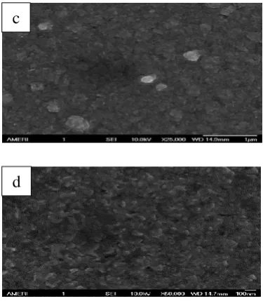
Figures 3a, 3b, 3c and 3d exhibits the surface view FE-SEM images of CZTS thin films deposited by sputtering technique from a single quaternary target. Figure 3a belongs to the as-deposited sample the surface of which looks dense without any bigger voids. Figure 3b exhibits a dense columnar morphology. This change in morphology as compared with Figure 3a may be due to the overgrown CuO at some parts of the film after annealing [20] and it is beneficial to decreasing the minority carrier recombination during transport process when applied to solar cell as observed by [13].
Figures 3c shows a densely-packed compact structure with some emerging grains. However, the CZTS thin film shown in figure 3d showed a dense microstructure with many voids located at middle and bottom region of the thin film. This difference in the void formation was attributed to the different Sn loss and diffusivity of Cu vacancy during annealing process as suggested by [10]. In addition, the Cu vacancy may be responsible for the formation of voids in the thin films.
Table 3 presents the energy dispersive x-ray (EDX) based on the atomic percentages results in which the elemental content of each sample has been analysed. There are deviations from the stoichiometric Cu2ZnSnS4
i.e. 1.0 for Zn/Sn and 1.0 for Cu/(Zn+Sn). These deviations can be defined as considerable deficiencies of Zn and Cu compared with the stoichiometry. It is not clear why this single target sputtering approach created such significant deficiencies in the absorber films, but it is assumed to be directly related to the different sputter yields and re-evaporation rates of elements during the active deposition of the film [28]. Zn percentage in the sputtered films were lower than that in the target. Such decrease should result from the Zn evaporation during sputtering since Zn has a high saturation vapour pressure. The excess of Sn should be the cause of SnS existence. It is known that if Zn/Sn 1 this specifies Zinc-rich sample. A sample is said to be Cu-poor if Cu/ (Zn+Sn) 1. If S 1 the sample is said to be S-poor. Figure 4 shows the relationship between the annealing temperature and the atomic %. All the samples are Zinc-rich.
200 300 400 500 600
Wave number (cm-1)
a
200 250 300 350 400 450
c
200 300 400 500 600
b
200 250 300 350 400 450
Figure 3: (a) as-deposited sample (b) sample annealed at 2500C (c) sample annealed at 3500C (d) sample
annealed at 4500C
TABLE 3:
EDX analysis results of randomly selected points on each sample
Sample Cu
at% Zn at%
Sn at%
S at%
CZTS 1 4.72 57.17 30.55 7.56 0.05 1.87 0.08
CZTS 2 13.47 49.92 22.93 13.68 0.18 2.18 0.16
CZTS 3 20.68 45.64 21.57 12.11 0.31 2.12 0.14
CZTS 4 25.52 44.07 18.63 11.77 0.41 2.37 0.13
Figure 4: Annealing temperature vs Atomic % for the samples
IV.
CONCLUSION
Researchers have focused on renewable energy from the sunlight, hydro, geothermal heat, and wind to supply humanity with energy alternatives. Photovoltaic is one of the sustainable and competitive energy sources. Copper zinc tin sulfide, Cu2ZnSnS4 (CZTS), has
received great interest because the compound consists of
earth abundant and nontoxic elements. This research focuses on the growth and characterization processes of CZTS thin films. XRD pattern revealed a highly crystalline tetragonal structure which corresponds to kesterite CZTS crystal. The compositions of CZTS crystals were homogeneous and were found to be highly Cu and S-poor. Most of the samples are Zn-rich. XRD is unable to accurately identify CZTS (wurtzite/kesterite) phases due to overlapping diffraction peaks. On the other hand in Raman spectroscopy, the characteristic vibrational modes of bulk CZTS (338 cm-1), Cu3SnS4
(318 cm-1), Cu2SnS3 (298cm-1), and Cu2−xS (269, 301,
and 470 cm-1) can be resolved reasonably well, and coexisting phases can be differentiated from each other. These experimental measurements corroborate the strong potential of Raman scattering for successful detection of secondary phases. In particular, this research demonstrate that secondary phases which cannot be distinguished by XRD based techniques can be detected. Some of the secondary phases detected are SnS, Cu SnS, ZnO, SnS and ZnS. According to the
0 10 20 30 40 50 60 70
0 200 400 600
At
o
mic
%
Annealing Temperature (C)
Cu at%
Zn at%
Sn at%
S at%
a
b
c
SEM results, an increase in the annealing temperature results in larger grains and grain boundaries. Although there are different schools of thoughts regarding the role of grain boundaries in thin film solar cells, it is generally accepted that grain boundaries act as recombination centres.
V.
ACKNOWLEDGEMENTS
The authors wish to acknowledge the financial support of TetFund through the management of Usmanu Danfodiyo University, Sokoto Nigeria. We also wish to thank Prof. Arvind Agarwal and clean room staff of the Advanced Materials and Engineering Research Institute (AMERI) of the Florida International University Miami, Florida U.S.A for technical support.
VI.
REFERENCES
[1]. K. K. Patel, Shah D.V and Vipul, K., "Effects of Annealing on Structural Properties of Copper Zinc Tin Sulphide (CZTS) Material". Journal of nano- and electronic Physics, vol, 5(3), pp. 1-4(2013) [2]. P. Bras, Sterner, J., & Platzer-Björkman, C.,
"Influence of hydrogen sulfide annealing on copper–zinc–tin–sulfide solar cells sputtered from a quaternary compound target". Thin Solid Films, vol. 582, pp. 233–238(2015).
[3]. S. Chen, X.G Gong, Walsh, A., & Wei, S. H., “Defect physics of the kesterite thin-film solar cell absorber Cu2ZnSnS4". Applied Physics Letters, vol. 96, pp. 8–10(2010).
[4]. T.K Todorov, T. K., Tang, J., Bag, S., Gunawan, O., Gokmen, T., Zhu, Y., & Mitzi, D. B., “Beyond 11% effi ciency: Characteristics of state-of-the-art Cu2ZnSnS(S,Se)4 Solar Cells". Advanced Energy Materials, vol. 3, pp. 34–38(2013a).
[5]. I.V Bodnar, Telesh, E. V., Gurieva, G., & Schou, J., “Transmittance Spectra of Cu2ZnSnS4 Thin Films". Journal of Electronic Materials, vol. 4, pp. 2–6(2015).
[6]. Q Guo, Grayson M. Ford, Wei-Chang Yang, Bryce C. Walker, Eric A. Stach, H. W. H. and R. A., “Fabrication of 7.2% Efficient CZTSSe Solar Cells Using CZTS Nanocrystals". J. Am. Chem. Soc, vol. 132, pp. 17384–17386(2010).
[7]. Y. Zhou, Zhou, W., Du, Y., Li, M., & Wu., S., “Sphere-like kesterite Cu2ZnSnS4 nanoparticles
synthesized by a facile solvothermal method". Materials Letters, vol. 65, pp. 1535–1537(2011). [8]. T. Tanaka, Yoshida, A., Saiki, D., Saito, K., Guo,
Q., Nishio, M., & Yamaguchi, T., “Influence of composition ratio on properties of Cu2ZnSnS4 thin films fabricated by co-evaporation". Thin Solid Films, vol. 518, pp. 29–33(2010).
[9]. H. Nukala, Johnson, J. L., Bhatia, A., Lund, E. A., Hlaing Oo, W. M., Nowell, M. M., Scarpulla, M. A., “Synthesis of Optimized CZTS Thin Films for Photovoltaic Absorber Layers by Sputtering from Sulfide Targets and Sulfurization". Materials Research Society Symposium Proceedings, vol. 1268, pp. 4–9(2010).
[10]. C. W Hong, Shin, S. W., Gurav, K. V., Vanalakar, S. A., Yeo, S. J., Yang, H. S., Kim., “Comparative study on the annealing types on the properties of Cu2ZnSnS4 thin films and their application to solar cells". Applied Surface Science, vol. 334, pp. 180–184(2015).
[11]. K.S Lim, Yu, S.-M., Khalkar, A. R., Oh, T.-S., Nam, J., Shin, D.-W., & Yoo, J.-B., “Comparison of Cu2ZnSnS4 thin films and solar cell performance using Zn target with ZnS target". Journal of Alloys and Compounds, vol. 650, pp. 641–646(2015).
[12]. P.A Fernandes, Salomé, P. M. P., Cunha, A. F., & Schubert, B., “Cu2ZnSnS4 solar cells prepared with sulphurized dc-sputtered stacked metallic precursors". Thin Solid Films, vol. 519, pp. 7382– 7385(2010).
[13]. F Liu, Li, Y., Zhang, K., Wang, B., Yan, C., Lai, Y., Liu, Y., “In situ growth of Cu2ZnSnS4 thin films by reactive magnetron co-sputtering". Solar Energy Materials and Solar Cells, vol. 94, pp. 2431–2434(2010).
[14]. T Tanaka, Nagatomo, T., Kawasaki, D., Nishio, M., Guo, Q., Wakahara, A., Ogawa, H., “Preparation of Cu2ZnSnS4 thin films by hybrid sputtering". Journal of Physics and Chemistry of Solids, vol. 66, pp. 1978–1981(2005).
[16]. C.P Chan, Lam, H., Wong, K. Y., & Surya, C., “Electrodeposition of Cu2ZnSnS4 Thin Films Using Ionic Liquids". Photovoltaic Materials and Manufacturing Issues, vol. 1123, pp. 105– 109(2009).
[17]. S.C Riha, Fredrick, S. J., Sambur, J. B., Liu, Y., Prieto, A. L., & Parkinson, B. A., “Photoelectrochemical characterization of
nanocrystalline thin-film Cu2ZnSnS4
photocathodes". ACS Applied Materials and Interfaces, vol. 3, pp. 58–66(2011).
[18]. T.S Shyju, Anandhi, S., Suriakarthick, R., Gopalakrishnan, R., & Kuppusami, P.,
Mechanosynthesis, deposition and
characterization of CZTS and CZTSe materials for solar cell applications. Journal of Solid State Chemistry, vol. 227, pp. 165–177(2015).
[19]. K Sun, Yan, C., Liu, F., Huang, J., Zhou, F., Stride, J. A, Hao, X., “Over 9% Efficient Kesterite Cu2ZnSnS4 Solar Cell Fabricated by Using Zn 1- x Cdx S Buffer Layer". Advanced Energy Materials. pp. 1-6(2016).
[20]. A.I Inamdar, Lee, S., Jeon, K. Y., Lee, C. H., Pawar, S. M., Kalubarme, R. S., Kim, H., “Optimized fabrication of sputter deposited Cu2ZnSnS4 (CZTS) thin films". Solar Energy, vol. 91, 196–203(2013).
[21]. J.P Leitão, Santos, N. M., Fernandes, P. a., Salomé, P. M. P., da Cunha, a. F., González, J. C., & Matinaga, F. M., “Study of optical and structural properties of Cu2ZnSnS4 thin films". Thin Solid Films, vol. 519, pp. 7390–7393(2011). [22]. A Osama & Cheng, Z., “In situ Raman
characterization of Cu2ZnSnS4 solar absorber material". IEEE 2015, pp. 1–6(2015).
[23]. B.T Jheng, Huang, K. M., Chen, S. F., & Wu, M. C., “Effects of substrate temperature on the Cu2ZnSnS4 films deposited by radio-frequency sputtering with single target". Thin Solid Films, vol. 564, pp. 345–350(2014).
[24]. V Parthibaraj, Tamilarasan, K., Pugazhvadivu, K. S., & Rangasami, C., “Growth and Characterization of Cu2ZnSnS4 Thin Film by RF-Magnetron Sputtering". Ijirset, vol. 4, pp. 670– 675(2015).
[25]. M. Abusnina, Moutinho, H., Al-Jassim, M., Dehart, C., & Matin, M., “Fabrication and characterization of CZTS thin films prepared by
the sulfurization of RF-sputtered stacked metal precursors". Journal of Electronic Materials, vol. 43, pp. 3145–3154(2014).
[26]. R. Ahmad, Distaso, M., Azimi, H., Brabec, C. J., & Peukert, W., “Facile synthesis and post-processing of eco-friendly, highly conductive copper zinc tin sulphide nanoparticles". Journal of Nanoparticle Research, vol. 15, pp. 1–16(2013). [27]. D.M Berg & Dale, P. J. 2014. “Kesterites :
Equilibria and Secondary Phase Identification". Pp. 107–132. Published 2015 by John Wiley and Sons Ltd.