Design of a reliable Bluetooth interface for
FPGA-based Embedded Systems
A. Giorgio* & F. Paris
Dipartimento di Ingegneria Elettrica e dell’Informazione – Politecnico di Bari – Digital Electronics Lab (eledigilab), Via E. Orabona, 4 70125 Bari, ITALY
*Corresponding Author E-mail: [email protected]
Abstract: Using the Field Programmable Gate Array (FPGA) based Embedded Systems (ES) for signal processing purposes, gives rise to the need to equip the FPGA of a Bluetooth (BT) connectivity if it does not have any. Therefore, the author has been designed an interface allowing an FPGA to hardware connect with the HC-05 BT module to communicate with any other BT device. The description of designed interface and of the test results are the object of this paper. The design has been performed using the Cyclone V FPGA by Altera. The test has been performed using the evaluation board DE1-SoC by Terasic. The test bench has been developed in MATLAB environment.
Keywords: FPGA, Embedded Systems, Digital Signal Processing, MATLAB. Bluetooth.
I. INTRODUCTION
The most recent practice in the design of Integrated Circuits (IC’s) for Digital Signal Processing (DSP) purposes, is strongly oriented towards a wide use of Programmable Logic Devices (PLD) [1], especially the Field Programmable Gate Arrays (FPGAs), and Embedded Systems (ES) designed using FPGAs due to their unique features of high performances at low cost [2-5], configured using Hardware Description Languages (HDLs) [6, 7]. It is also possible to design a complete ES in both its software and hardware part using the only FPGA chip [8].
Anyway, most of FPGAs are not equipped with a Bluetooth (BT) plug-in and then a serious problem arises if a BT connectivity is required. Therefore, in this letter, it is described the design of an interface allowing the FPGA to connect with the HC-05 BT module and communicate via BT with other devices. There are addressed the main design techniques adopted to improve the reliability of data transmission via BT. The specific FPGA (5CSEMA5F31C6) used for the design belongs to the Cyclone V family by Altera. Anyway, the design approach is quite general and useful for other FPGAs families and brands.
II. DESCRIPTIONOFTHEDESIGNEDBLUETOOTHINTERFACE
The BT connection adopts the UART communication protocol. Therefore, the designed interface allows the communication by the UART protocol (with any UART transmitters and receivers) choosing between various baud rates ranging from 2400 to 921600 baud.
The design is a complete transceiver and therefore is composed of two modules, the BT receiver and transmitter.
A. Bluetooth Transmitter for FPGA
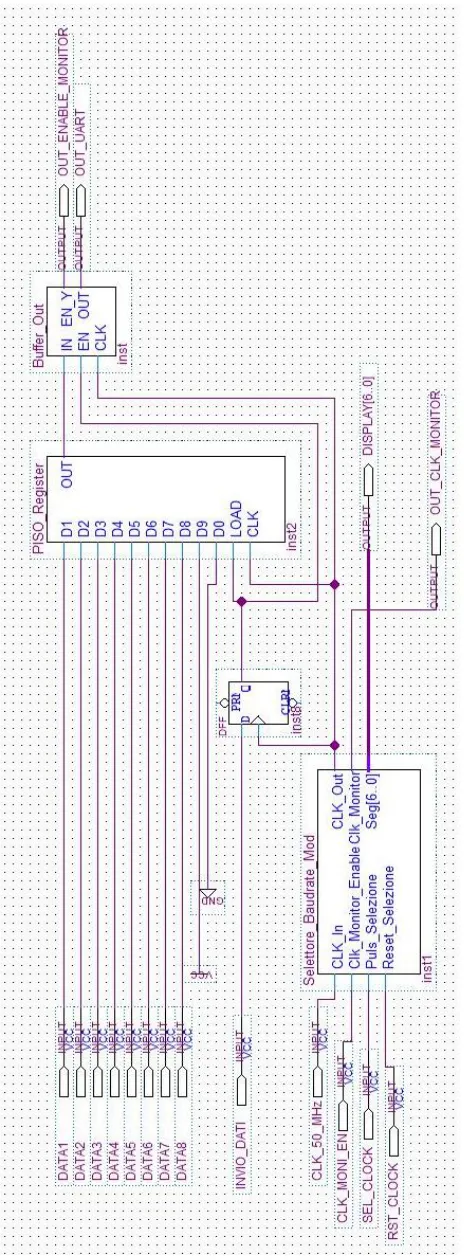
edge of the INVIO_DATI signal corresponds to the rising edge of the clock. On the contrary, we verified that no data loss occurs if the INVIO_DATI signal rising edge corresponds to the main clock falling edge. Therefore, the D-type Flip-Flop stores the value of the INVIO_DATI signal for the whole clock period and then forbids the INVIO_DATI rising edge to be in correspondence of the main clock rising edge. Moreover, as fig. 1 shows, the transmitter is equipped also with a baud-rate selector to choose between nine options: 2400/4800/9600/19200/38400/57600/115200/230400/460800/921600 Baud. The SET_CLOCK input allows the Baud rate selection; the RESET_CLOCK one allows resetting the selection. The 7-segment display shows the selected baud rate option (1st, 2nd, 3th, etc. option).
For testing purposes, any one-byte data packet to send is set using 8 switches on the evaluation board DE1_SoC. Transmission module inputs, their functions and PIN assignments are:
- CLK_50 is connected to the 50 MHz internal clock of the DE1_SoC, which pin name is AF14;
- DATA1..DATA8 are the data inputs provided for test purposes by 8 switches on the DE1_SoC board and these are identified with pin AB12 / AC12 / AF9 / AF10 / AD11 / AD12 / AE11 / AC9.
- For INVIO_DATI inputs (pin Y16), SET_CLOCK (pin AA15), RESET_CLOCK (pin AA14) we have used pushbuttons on DE1_SoC board. It is noticeable that pushbuttons are active low, therefore it will be necessary to use a logic NOT gate for proper positive logic operation;
- CLK_MONI_EN (Clock Monitor Enable) input, if set to a high logic value will activate the OUT_CLK_MONITOR output that will provide the clock signal corresponding to the selected baud rate.
Transmission module Outputs, their functions and pin assignments are:
- OUT_UART output provides the serial signal to transmit according to the UART protocol. This output must be connected to the BT module HC-05 input and the assigned pin is the GPIO_0[0] of DE1-SoC, whose value is PIN_AC18;
- DISPLAY_TX H0 [6..0] are the seven bus lines connected to the seven-segment display on the board. The assigned pins are AD27, AF30, AF29, AG30, AH30, AH29, AJ29.
- OUT_CLK_MONITOR output, activated by the signal CLK_MONI_EN, provides the clock signal at the selected baud rate to other modules in the design or simply for debug purposes;
F
ig. 1. S
che
matic of
the tr
ansmi
tt
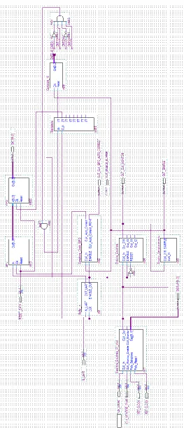
As in the case of the transmitter module, also the receiver module is equipped with a 50MHz clock input and a baud rate selector with relative 7-segment display to view the selection.
Fig. 2 shows the schematic of the receiver. The design of the receiver proposed in this letter addresses and solves many problems typical of the UART protocol communication, making more reliable the BT data transfer. The first problem solved is the synchronization between the active edge of the clock of the receiver and the start bit of the incoming data stream (10 bits per packet). To this aim has been designed an input circuit able to place the active edge of the clock of the receiver at the middle of the duration of each of the incoming bits, avoiding any data losses. In fact, the clock is multiplied by 16 and a proper internal signal, switching from 0 to 1 as the input start bit arrives, forces the CLKx16 signal to start the sampling. Then, a counter act as frequency divider for the CLKx16 signal and the output of the counter returns a new clock signal of the right frequency which active edge is placed at the middle of each incoming bit.
The further building block of the receiver is a Serial Input Parallel Output (SIPO) register able to convert the serial data stream in a parallel one-byte package. Finally, there is the baud rate selection circuit, the same of the transmitter.
The typical architecture of a SIPO register has been modified to improve the BT data transfer. In fact, the SIPO register places the 8-bits packet as parallel output after 10 clock shots, i.e. at the 11th clock shot, but this implies a bad sampling of the next input start bit and data missing can occur. To solve this problem, it has been modified the timing of the circuit so that the SIPO register produces its output byte at the 10-th clock shot and it has been cascaded a Parallel Input Parallel Output (PIPO) register to hold 10-the parallel byte on the output line of the receiver. So that the SIPO register, can sample and convert the next stream of 10-bits without any data loosing.
F
ig. 2. S
che
mati
c of the
r
ec
eive
r de
signed in Qu
ar
tus environme
- RESET_DATA input allows resetting registers storing the parallel one-byte stream. The pin assignment value is that of a pushbutton available on the DE1_SoC, i.e. the PIN_W15.
Receiver module Outputs, their functions and pin assignment on the DE1_SoC evaluation board are:
- DATA [9..0] outputs are for debugging purposes allowing to switch on or off the LEDs available on the DE1_SoC board according to the value of each of the received 10-bits package is 1 or 0. They are included the start bit (DATA [0]) and the stop bit (DATA [9]). The bit from DATA [8] to DATA [1] are the one-byte data packet. Therefore, for debug purposes, these last 8 lines are assigned pins of the 8 LEDs on the DE1_SoC board: V16, W16, V17, V18, W17, W19, Y19, W20;
- DISPLAY [6..0] outputs are for displaying the selected baud rate on the second seven-segment display available on the DE1_SoC board. The related assigned pins are: AH28- AG28, AF28, AG27, AE28, AE27, AE26.
- OUT_CLK_MONITOR output provides the clock signal according to the selected baud rate. The pin assignment is arbitrary.
- OUT_ENABLE_BUFFER output provides a square wave signal whose duration is equal to the time window of 10 bits in which the receiver samples each incoming 10-bits packet. It is activated each time arrives a start bit. It is useful for testing purposes or as a sync signal for other devices. The pin assignment is arbitrary.
- OUT_CLK_SIPO_AUTO_CORRECT output is the sync-corrector signal and is useful to export it for debug purposes. The pin assignment is arbitrary.
- OUT_SAMPLE output provides the sampling signal of the input line. The pin assignment is arbitrary
III. RESULTS
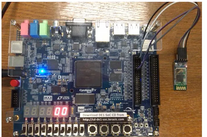
The test of the designed BT transceiver has been performed using the DE1_SoC evaluation board and equipping the Cyclone V FPGA with the BT module HC-05 connected with the FPGA by the GPIO on the DE1_SoC, as previously stated. Then, there were connected via BT the FPGA+HC-05 as with a Personal Computer (PC) and then with an Android smartphone, as the fig. 3 shows.
The connections between the GPIO_0 of the DE1-SoC board and the pins of the HC-05 module are:
- RXD (HC05) -> GPIO_0 [0] (DE1-SoC) pin 1;
- TXD (HC05) -> GPIO_0 [1] (DE1-Soc) pin 2;
- DC 5V (HC05) -> GPIO_0 VCC5 pin 11;
Fig. 3. Connections for testing purposes
Fig. 4 shows a photo of the test setup. Once the BT interface has been programmed into the FPGA by using the Quartus programmer tool, and the HC-05 has been connected, the test starts transmitting and receiving data via BT with a PC and then with a smartphone.
Firstly, it is necessary to select the baud rate pressing the pushbutton SET_CLOCK. To use the 9600 baud rate press the SET_CLOCK until the display shows the "22" code.
Fig. 4. Test setup for the designed interface: DE1_SoC evaluation board with the Cyclone V FPGA in the middle, and HC-05 Bluetooth module connected via GPIO expansion header provided by the
DE1_SoC.
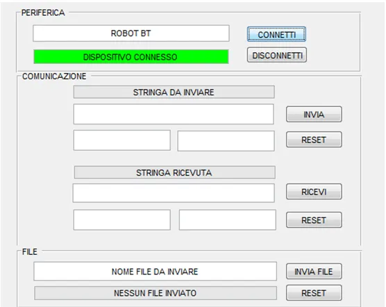
Fig. 5. MATLAB GUI developed for testing purposes able to exchange strings, bits and files via BT between a PC and the FPGA equipped with the HC-05 module
The GUI allows transmitting and receiving bits, strings and files and the test was successfully.
On the DE1_SoC board it is possible to see any received byte in a binary form through 8 red leds available. If a received bit = 0 the corresponding led turns off; if bit = 1 the corresponding led turns on. To set a byte to send from the FPGA to the PC there are used 8 switches available on the DE1_SoC board. Switch off means bit = 0, switch on means bit = 1.
The MATLAB GUI allows seeing the received data in the binary form and this allows verifying the correctness of the transmission. To test the BT interface with a smartphone also, the author developed a GUI using the Bluetooth Electronics app powered by KEWLSOFT (in Google play store). Once more all tests of data transfer via BT between the FPGA and the smartphone were successful.
IV. CONCLUSIONS
In this letter, it has been described an interface designed to allow a reliable communication via BT between an FPGA and any BT device. Many problems of UART transmission have been addressed and solved using specific design solutions. The designed interface allows the FPGA without a BT plug-in to be equipped with an external BT module. The design has been successfully simulated. Moreover, tests of data transfer have been performed connecting the FPGA with a PC and with a smartphone and all were completely successful. The conclusion is that the designed interface allows a reliable and fault-free data transfer allowing the FPGA acting as a BT receiver as a BT transmitter.
Conflict of interest: The authors declare that they have no conflict of interest.
Ethical statement: The authors declare that they have followed ethical responsibilities.
REFERENCES
[1] A. Giorgio, “Dispositivi Logici Programmabili” in Lezioni di Fondamenti di Elettronica dei Sistemi Digitali, 1st ed, Roma Italy, Gruppo Ed. L’Espresso, 2016, pp. 251-270
[2] C. Brandolese, W. Fornaciari, “Tecnologie Hardware” in Sistemi Embedded, 1st ed., Milano Italy, Pearson
[3] Intel Corporation (February 2017), Altera, Nios II processor, Available: https://www.altera.com/products/processors/overview.html
[4] Altera Corporation (February 2012), SoC FPGA ARM Cortex A9 MPCore Processor Advance Information Brief. Available: https://people.ece.cornell.edu/land/courses/ece5760/DE1_SOC/aib-01020-soc-fpga-cortex-a9-processor.pdf
[5] M. J. S. Smith, (November, 14, 2004), Addison Wesley, [online] Available:
https://archive.org/stream/ApplicationSpecificIntegratedCircuitsAddisonWesleyMichaelJohnSebastianSmith/
Application-Specific%20Integrated%20Circuits%20-%20Addison%20Wesley%20Michael%20John%20Sebastian%20Smith#page/n0/mode/2up
[6] S. Brown, Z. Vranesic, (2009), Fundamentals of Digital Logic with VHDL Design (3rd ed.), McGrawHill,
[online] Available:
https://archive.kottnet.net/Academic-Life/KTH/Fundamentals%20Of%20Digital%20Logic%20With%20VHDL%20Design%203rd%20Edition.p df
[7] S. Palnitkar, (March, 3, 2003), Verilog HDL: A Guide to Design and Sinthesys (2nd ed.), Prentice Hall,
[online] Available the 1st ed.: http://www.1apps.com/electronicsengg/books/Verilog%20HDL%20
-%20Samir%20Palnitkar.pdf
[8] P. Marwedel, (2011), Embedded Systems Design, (1st ed.), Springer Science
[9] Altera Corporation (2016), Software Download Available: https://www.altera.com/downloads/download-center.html
[10] Altera Corporation (2016), Embedded Systems Training Tutorials, Available:
https://www.altera.com/support/training/university/material_embedded_systems.html