SINGLE OTRA BASED PD
CONTROLLERS
RAJESHWARI PANDEY
Department of Electronics and Communication Engineering , Delhi Technological University ,
Shahbad Daulatpur, Bawana Road, Delhi, 110042, India
SAURABH CHITRANSHI
Department of Electronics and Communication Engineering , Delhi Technological University ,
Shahbad Daulatpur, Bawana Road, Delhi, 110042, India
NEETA PANDEY
Department of Electronics and Communication Engineering , Delhi Technological University ,
Shahbad Daulatpur, Bawana Road, Delhi, 110042, India
CHANDRA SHEKHAR
Department of Electronics and Communication Engineering , Delhi Technological University ,
Shahbad Daulatpur ,Bawana Road, Delhi, 110042, India
Abstract:
This paper presents a single Operational transresistance (OTRA) based voltage-mode proportional-derivative (PD) controller with independent tuning of proportional (Kp) and derivative (Kd) constants. This configuration can be made fully integrated by implementing the resistors using matched transistors operating in linear region. In order to verify the proposed circuit a closed loop control system using the proposed PD controller is designed and simulated using SPICE.
Key Words: OTRA, MOS implementation of a linear resistance, PD Controller, Second order LPF.
1.
IntroductionThe derivative (D) controllers with adjustable parameters are used to control integrating systems and systems with inertia. In either situation, pure derivative control is not used, for it is too fragile. Instead, proportional and derivative controls are mixed together to maximize the stability. Motor control and robot manipulators are examples of PD controllers.
Reference [3] presents OTA based controllers and [4] presents CDBA based controllers whereas CCII based controllers are proposed in [5]-[7]. In this paper an OTRA based controllers has been presented.
It is well known that inherent wide bandwidth which is virtually independent of closed loop gain, greater linearity, and large dynamic range is the key performance features of current mode technique [8]. Operational Transresistance Amplifier (OTRA) is a high gain current input, voltage output amplifier [9]. OTRA, being a current processing analog building block, inherits all the advantages of current mode technique. It is also free from parasitic input capacitances and resistances as its input terminals are virtually grounded and hence, non-ideality problem is less in circuits implemented using OTRA. Several high performance CMOS OTRA topologies have been proposed in literature [9]-[12] leading to growing interest in OTRA based analog signal processing circuits. In recent past OTRA has been extensively used as an analog building block for realizing a number of signal processing circuits such as filters[13]-[16], oscillators[17]-[19], multivibrators [20],[21] and immittance simulation circuits[17],[22]-[24].
This paper aims at presenting a PD controller using single OTRA two resistors and a capacitor having orthogonally tunable proportional and derivative constants. These circuits can be made fully integrated by implementing the resistors using MOS transistors operating in non-saturation region.
2. Circuit Description
2.1.PD controller
In PD controller as shown in Fig.1, the actuating signal, a(t) is sum of proportional to the error signal, e(t) and the derivative of e(t). Representing in s-domain can be written as
G s K K s (1)
where KP and Kd are the proportional and derivative constants, respectively.(1) can alternatively be represented as
G s K 1 T s (2)
where Td=Kd / Kp. The amplitude M(ω) and phase Ф(ω) characteristics of (2) are given by
M ω K 1 ωT (3)
Ф ω arctg ωT (4)
2.2.OTRA based PD controller
OTRA is a three terminal device [10] shown symbolically in Fig.2 and its port relations can be characterized by matrix (5).
V V V
0 0 0
0 0 0
R R 0
I I
I (5)
For ideal operations the transresistance gain Rm approaches infinity and forces the input currents to be equal. Thus OTRA must be used in a negative feedback configuration [9],[10].
Fig. 2.OTRA Symbol
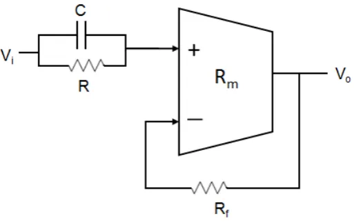
Proposed PD controller is shown in Fig. 3. The routine analysis of this controller gives the following voltage transfer function
sCR (6)
And results in
K K CR (7)
From the above equation it is clear that by varying R, Kp value can be adjusted independent of Kd and by simultaneous variation of Rf and R, Kd can be independently controlled.
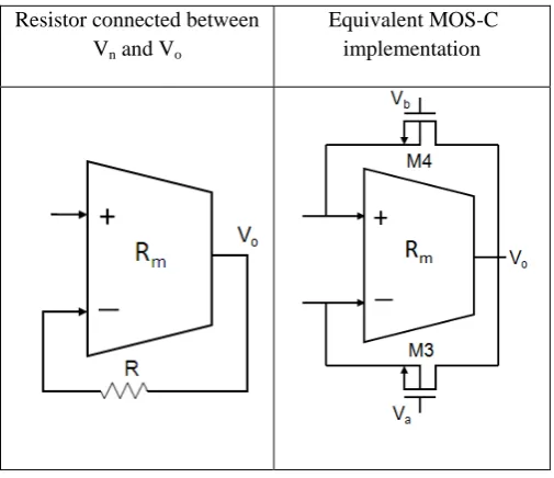
These parameters can be electronically tuned by implementing the linear passive resistors using MOS transistors operating in non-saturation region. The resistance value may be adjusted by appropriate choice of gate voltages.
Resistor connected between Vn and Vo
Equivalent MOS-C implementation
Fig. 4. MOS implementation of a Linear resistance.
The resistors connected to the input terminals of OTRA can easily be implemented using MOS transistors with complete non-linearity cancellation [10]. Fig. 4 shows a typical MOS implementation of resistance connected between negative input and output terminals of OTRA.
The equivalent resistance value is given as
R 1
μ C WL V V (8)
where μn, Cox, W and L are electron mobility, oxide capacitance per unit gate area, effective channel width,
and effective channel length respectively which may be expressed as
μ (9)
C (10)
W W 2W (11)
L L 2L (12)
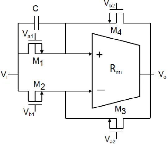
Va and Vb are the gate voltages and other symbols have their usual meaning. Fig. 5 shows the MOS-C implementation of the circuit of Fig.3.
3.Non-Ideality Analysis
Fig. 5.MOS-C equivalent of Proposed PD Controller
3.1Non- Ideality due to Finite Transresistance Gain
Here the effect of finite trans-resistance gain (Rm) on PD controller is considered and for high frequency
applications passive compensation is employed. Ideally the Rm is assumed to approach infinity. However,
practically Rm is a frequency dependent finite value. Considering a single pole model for the trans-resistance gain, it can be expressed as
R (13)
where R0 is dc transresistance gain.
For high frequency applications the trans-resistance gain, reduces to
R s where C (14)
Taking this effect into account (6) modifies to
o sC
(15)
For high-frequency applications, compensation methods must be employed toaccount for the error introduced in (4). Considering the circuit shown in Fig.6, equation (15) modifies to
o
(16)
By taking Y = Cp, (16) reduces to (6). The effect of Rm can thus be eliminated by connecting a single capacitor
Fig. 6.Compensated PD Controller Fig. 7 AC equivalent of proposed PD Controller
3.2 Effect of Nonzero Impedances of p and n Terminals
Ideally input as well as output resistances are assumed to be zero. To consider the effect of and non zero values of input resistances (Rn and Rp) and output resistances (Rout1) on proposed PD controller AC equivalent of the
controller using AC equivalent of OTRA is drawn and is shown in fig 7.
Routine analysis of Fig. 6(a) results in terminal currentsIp and In as
I (17)
I (18)
Thus the output voltage Vo can be written as
V R I I R I (19)
V R I R R I (20)
As Rm >>Rout1 so Rm+Rout1≈Rm and hence
V R I I (21)
Substituting Ip and In,(21) results in
V R (22)
(23)
As R>> Rp, Rm >> (Rf +Rn) and Rf >>Rn and so (23) yields
(24)
Comparing (25) with (6) it is observed a parasitic pole with pole frequency 1/RpC is introduced. The parasitic
pole frequency would be much beyond the zero frequency (1/CR) for a selection of R>>Rp, and would not
influence the performance of the system.
4. Simulation Results
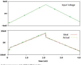
In order to verify the theoretical propositions simulations are performed using PSPICE program. For simulation CMOS implementation of the OTRA proposed in [12] was used. The SPICE simulation was performed using 0.18µm, Level 7, CMOS process parameters provided by MOSIS and supply voltages taken are ±1.5 V. For the proposed controller shown in Fig. 3, the values of passive element are chosen as R = 10KΩ, Rf =
20KΩ and C = 20pF.For time domain analysis, a 3mV peak triangular input voltage is applied. For this input the output of the proposed controller would be given by
V t . V t CR (26)
Both ideal and simulated results are presented in Fig. 8a and are found in agreement with (26). In the magnitude response of the proposed controller given by (3) first term is dominant for low frequencies (ω << 1/Td) and thus would result in a constant output (≈20 log Kp) whereas for high frequencies (ω >> 1/Td) the
second term of the response becomes effective and the output would be represented by a straight line having a slope of 20dB/decade. Similarly for phase response for low frequencies phase would be 0° ,atω = 1/Td it would
be 45° and would approach 90° for extremely high frequencies. It is observed that the frequency domain response of the proposed controller shown in fig.8b is in close agreement to above discussion.
Fig. 8b. Frequency and phase Response of PD controller.
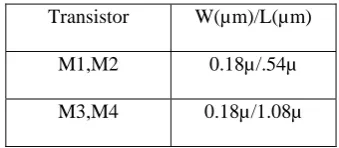
For MOS-C implemented PD controller shown in Fig 5 the aspect ratios of the transistors used for implementing the resistances are listed in Table.1.
Table1.Aspect ratios of transistors used for resistance implementation
Transistor W(µm)/L(µm)
M1,M2 0.18µ/.54µ
M3,M4 0.18µ/1.08µ
Gate voltages are set as Va1= Va2 = 1.2V and Vb1=0.59V, Vb2 =0.64V which result in resistance values as R
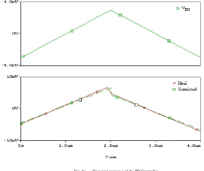
≈10KΩ Rf≈20KΩ and the chosen value of C = 20pF.The ideal and simulated time domain response of MOS-C
Fig. 9a.Transient response of the MOS-C PD Controller.
Fig. 9b.Frequency and phase Response of the MOS-C PD Controller.
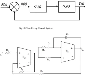
Fig.10.Closed Loop Control System.
Fig. 11.Second order Low Pass filter.
The transfer function of the LPF is given as
(27)
Where K=Ra/Rb. The values of passive element for the filters are selected as Ra=Rb =20KΩ, R1=2KΩ, and
C1= C2=20pFwhich result in
. ∗
∗ . ∗ (28)
Now a PD controller, with the component values R=5K, Rf=15KΩ and C=8pF resulting in KP=3 and
Kd=0.12×10⁻⁶s is added to form control system of Fig. 10.
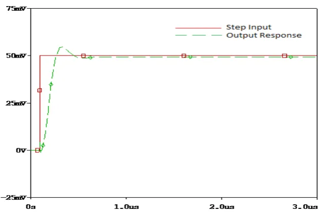
Fig. 12a.Step Response of a second order system without PD controller.
Fig.12b.Step Response of a second order system with PD controller.
Performance comparison of second order system with and without PD controller is shown in Table. 2. It is clearly visible from the table 2 that the response of the system has been improved.
Table. 2. Performance Comparison.
Parameter Without PD
Controller
With PD Controller
Overshoot 19.56% 10.59%
Peak
output 58.26mV 54.63mV
Conclusion
A single differential Operational transresistance (OTRA) based voltage mode proportional-derivative (PD)
controller has been presented which possesses the feature of independent tuning of proportional (Kp) and derivative (Kd) constants. This controller can be made fully integrated by implementing the resistors using MOS transistors operating in linear region. As an application, a second order closed loop system is designed and simulated using SPICE program. The simulated results are in line with the proposed theory.
Reference
[1] S. Franco, Design with operational amplifiers and analog integrated circuits. Singapore: Mcgraw-Hill International Edition, 1998. [2] M.T. Kara, and M.E. Rizkalla, “Single op-amp proportional-integral compensator with anti-windup,” In Proceedings of the IEEE
International Symposium on Circuits and System. Chicago, Illinois, (USA)1993, pp. 2260 - 2263.
[3] C. Edral, A. Toker, and C. Acar, “OTA-C based proportional- Integral-derivative (PID) controller and calculating optimum parameter tolerances,” Turkish journal of Elec, vol. 9, no. 2, Nov. 2001, pp.189-198.
[4] A.U. Keskin, “Design of a PID controller circuit employing CDBAs,” International Journal of Electrical Engineering Education, vol. 43, no.1, Jan. 2006, pp.48-56.
[5] S. Minaei, E. Yuce, S. Tokat and O. Cicekoglu, “Simple realization of current-mode and voltage mode PID, PI and PD controllers,” In
Proceeding of IEEE ISIE. Dubrovnik (Croatia)June 2005, pp.195-198.
[6] E. Yuce, S. Tokat, S. Minaei and O. Cicekoglu, “ Low-Component-Count Insensitive Current-Mode and Voltage-Mode PID, PI and PD Controllers,” Frequenz, vol.60, no. 3-4, April 2006, pp. 65-69.
[7] V. Michal, C. Prémont, G. Pillonet and N. Abouchi, “Single Active Element PID Controllers,” In Proceedings of the Radioelektronika 20th International Conference. CPE-Lyon, Villeurbanne (France) April 2010, pp. 1 – 4.
[8] C. Toumazou, F. J. Lidgey and D. G. Haigh, “Analogue IC Design: The Current Mode Approach,” U.K.: Peregrinus, 1990.
[9] J. Chen, H. Tsao and C. Chen, “Operational transresistance amplifier Using CMOS Technology,” Electronics Letters, vol.28, no.22, Oct. 1992, pp. 2087–2088.
[10] K.N. Salama and A.M. Soliman, “CMOS operational transresistance amplifier for analog signal processing,” Microelectronics Journal, vol.30 no. 3, March 1999, pp. 235–45.
[11] H. Mostafa and A.M. Soliman, “A Modified CMOS Realization of the Operational Transresistance Amplifier (OTRA),” Frequenz,
vol.60, No: 3-4, April 2006, pp. 70 -76.
[12] A. K. Kafrawy and A.M. Soliman, “A modified CMOS differential operational transresistance amplifier (OTRA),” AEU-International Journal of Electronics and Communications, vol. 63 no. 12, Dec. 2009, pp. 1067-1071.
[13] S. Kilinc, A. U. Keskin and U. Çam, “Cascadable Voltage-Mode Multifunction Biquad Employing Single OTRA,” Frequenz, vol. 61, No: 3-4, April 2007, pp.84-86.
[14] K.N. Salama and A.M. Soliman, “Universal Filters Using Operational Transresistance Amplifiers,” AEU-International Journal of Electronics and Communications, vol.53, no. 1, Jan. 1999, pp. 49-52.
[15] J. Chen, H. Tsao and S.I. Liu, “Parasitic- capacitance-insensitive current-mode filters using OTRA,” IEE Proc.-Circuits Devices Syst.,
vol. 142, no. 3, June 1995, pp.186-192.
[16] A. Gokcen and U. Cam, “MOS-C single amplifier biquads using the OTRA,” AEU-International Journal of Electronics and Communications, vol. 63 no. 8, Aug.2009, pp. 660-664.
[17] K.N. Salama and A.M. Soliman, “Novel oscillators using operational transresistance amplifier,” Microelectronics Journal, vol.31, no.1, Jan. 2000, pp. 39-47.
[18] U. Cam, “A Novel Single-Resistance-Controlled Sinusoidal Oscillator Employing Single Operational Transresistance Amplifier,”
Analog Integrated Circuits and Signal Processing, vol. 32, no. 2, Aug. 2002, pp. 183-186.
[19] R. Pandey, N. Pandey, M. Bothra and S.K. Paul, 2011,May . Operational Transresistance Amplifier-Based Multiphase Sinusoidal
Oscillators. Journal of Electrical and Computer Engineering. Volume 2011,Available:
http://www.hindawi.com/journals/jece/2011/586853/
[20] C.L. Hou, H. C. Chien, and Y. K. Lo, “Squarewave generators employing OTRAs,” IEE proc.-Circuits Devices Syst., Vol.152, no. 6, Dec. 2005, pp. 718–722.
[21] Y. K. Lo, H. C. Chien and H. G. Chiu, “Switch Controllable OTRA Based Bistable Multivibrator,” IET Circuits Devices Syst., vol. 2, no. 4, Aug. 2008, pp. 373–382.
[22] U. Cam, F. Kacar, O. Cicekoglu, H. Kuntman and A. Kuntman, “Novel grounded parallel immittance simulator topologies employing single OTRA,” AEU-International Journal of Electronics and Communications, vol. 57, no.4, 2003, pp. 287-290.
[23] S. Kilinc, K. N. Salama and U. Cam, “Realization of fully Controllable negative Inductance with single operational Transresistance Amplifier,” Circuits Systems Signal Processing, vol. 25, no.1, Feb. 2006, pp.47-57.
[24] U. Cam, F. Kacar, O. Cicekoglu, H. Kuntman and A. Kuntman, “Novel two OTRA-based grounded Immittance simulator topologies,”
Analog Integrated circuit and Signal Processing, vol. 39 no. 2, May 2004, pp.169-175.