A STRATEGY FOR ASSESSING THE
STABILITY OF SEPIC CONVERTER
A.EZHILARASI* M.RAMASWAMY
Sr. Lecturer Professor
Department of Electrical Engineering,
Annamalai University, Annamalainagar, TamilNadu-608002
ABSTRACT
A strategy is coined with a view to assess the stability margin of a SEPIC Converter. The small signal model of the SEPIC Converter is developed, which allows selection of control coefficients, analysis of parameter variation effects and characterization of the closed-loop behavior in terms of the ratio of its output to duty cycle transfer function. The eigen values of the characteristics equation provide the small-signal stability properties of the system. It is envisaged to incorporate an appropriate compensator in order to aid in the process of accomplishing a stable operation of the Converter. The performance is evaluated through MATLAB based simulation and includes both Root locus and Bode plot analysis to demonstrate the suitability of the use of compensator to encompass the SEPICs stable operation over a desired load range.
KEY WORDS: Stability, Compensator, Root locus, Bode plot
INTRODUCTION
The field of Power Electronics continues to pose challenging problems in the sense its region of operation and the range of load it can support require specific modeling and controller design approaches. The main difficulty arises from the hybrid nature of these systems due to the presence of semiconductor switches that induce different modes of operation and operate at a high switching frequency [1]. The control techniques traditionally employed offer a significant potential for improving the performance and the design of controllers. However the need for advanced hybrid systems methodologies exists due to the varying degree of performance.
The computational power available today and the recent theoretical advances in the control of hybrid systems facilitate to tackle these problems in a systematic and cohesive manner. Frequency response analysis techniques are among several ways of determining the stability and robustness of the closed-loop DC-DC converter [2]. These techniques can be effectively adapted to objectively acquire a set of frequency response functions to determine the stability of power converters besides its output voltage regulation. It is performed analytically through Modeling and Simulation.
A host of control techniques are in useover the last three decades, the most satisfying among them is the role of conventional feedback controllers [3]. The advent of intelligent computations has enabled the use of Power Converters for real time applications. However the stability analysis still continues to evolve and requires to be addressed in its totality. Though continuous efforts are in vogue to device new control schemes suitable for switching converters, to extract a stable operation, ensure tight output voltage regulation and dynamic response, the use of compensators appear to evince keen interest and promise attractive results. It is in this direction that a compensator based strategy is proposed to determine the stability of SEPIC Converter.
The primary objective is to model a feedback compensator in order to ensure the stable operation of a SEPIC Converter. It involves the construction of the small signal model of SEPIC, from where its transfer function model is developed to aid in the process of determining its stability. The approach aims to evaluate the steady state stability using both Root locus and Bode plot through MATLAB based simulation. Besides it attempts to regulate the load voltage through an appropriate correction in the duty cycle of the power modulator.
PROPOSED STRATEGY
The power module of the DC-DC SEPIC Converter seen in Fig.1 can either step up or step down the input voltage, while maintaining the same polarity and the ground reference both for the input and output.When the power switch is turned on the first inductor, L1, is charged from the input voltage source and allows the second inductor to draw energy from the first capacitor, leaving the output capacitor to provide the load current. When the switch is turned off, the first inductor charges the capacitor C1 besides delivering current to the load. The second inductor is observed to be connected to the load.
MODELING
Models play a significant role in the development of complex system on account of the fact they facilitate a better understanding of variables and parameters affecting the system performance. Besides it serves as a tool to include new devices and predict its behavior almost instantaneously. Modeling and analysis of switching DC-DC Converters can be either numerical or analytical. A host of algorithms or circuit simulators are used to produce quantitative results in numerical approaches. Though they posses accuracy and universality and are applicable even when no equivalent model is available they are time-consuming and fail to provide the design insight needed to understand the behavior of switching regulators.
Analytic techniques, on the other hand, use analytic expressions to represent the operation and there from extract the performance of the converters. The inherent switching operation of power electronic converters results in the circuit components being connected together in periodically changing configurations, each configuration being described by a separate set of equations. The most popular continuous-time technique is the small-signal analysis, which uses circuit averaging [11], state-space averaging [12], or PWM switch modeling [13].
Small signal modeling is a common technique used to approximate the behavior of non linear devices with linear equations. The linearization is considered around the DC bias point of the device and accurate for small excursions about this point. The small signal model of a SEPIC Converter is derived as a transfer function ratio of output to duty cycle.
Fig.2
The transfer function of the chosen lead lag compensator shown in figure 2 is
2
2 '2
1 2 2
1 1 1
' 2 2 1
'2 2 2
2 2
01 1 01 02 2 02
01 2
'2
1 2 1 2 1 2
2 1 '2 1 2 01 02
1 1 1 1 2 '2
2
( ) 1 1
( ) 1 ( ) 1 1 1 1 1 R D Vo S
d S S S
where
R
D
SL
SC
L L
RD
S
L
C
L
D
D
D
S
S
Q
Q
D
C
C
C C
L
L
D
Q
D
L
L
D
C
C
L
L
D
D
2 2 2 01 1 2 1 2 02 2 02 RC C
Q
C
L L
C
….(2)
The overall transfer function is obtained by multiplying expression (2) with (1).
2 '2 2 1 2 1 2 1 1 '2 2 1 02 2 2
2 2
01 1 01 02 2 02
' 2 2 2
1
1
1
1
.
1
1
1
1
0.5
m z c PL s PL c ACS
R
D
S
S
S
S
where
SC L L
SL
D
RD
S
L
C
K
L
D
D
V
V
D
S
S
Q
Q
T
m D
C
C
R
L
2 21 2 3
2 2 3
1 2 3
2
2 2 3 1 1 . . ( ) . 1 1 1 ( ) z m p m z p S R C R C C S S
R C C S
K S K
R C C C
R C C
Fig.3
The parameters FM is the modulator gain of PWM, Ri is the dc gain of current sensing network, He(s) is the sampling gain of the same current sensing network, Kr is the feedback gain created by current feedback and Fv is the transfer function of the compensator. The switching strategy is designed to generate a PWM pulse for the switch in the Converter in accordance with the inputs from the Current Sensing Network (CSN), the compensating network and the output voltage. The values of the duty cycle (D) and those of the small signal voltage and current sources are appropriately chosen keeping in mind the nature of operation of the converter (Buck/Boost) and the range of load over which the Converter is desired to deliver power.
SIMULATION RESULTS
MATLAB is a state-of-art mathematical software package, which is used to extensively to perceive and predict the performance of systems over a range of operating states. It is an interactive program for numerical computation, which along with its programming capabilities serves as a very useful tool. It aids to display information graphically.
The scheme is simulated using MATLAB SIMULINK. A Buck/Boost SEPIC Converter with the following parameters R1 = 1e-3 , L1 = 100 H, R2 =1e-3, L2 = 100 H, R1 = 3e-3 C1 = 680 F, R0 = 1e-3 , C0 = 200 F, switching frequency = 50 kHz and a load allowed to vary up to 5000 Watts is chosen for investigating its stability. It is desired to obtain an output of 230 V from an input of 350 V for Buck converter and 350 V for Boost converter from an available input of 230 V.
Fig.4
Fig.5
STABILITY ANALYSIS
The second part of this paper focuses its attention to investigate the steady state closed loop stability of both Buck and Boost SEPIC Converter. The basic philosophy is to guarantee its output voltage regulation and ensure its stability through the use of a lead lag compensator over a range of operating states.
The root locus is the locus of the roots of the characteristic equation of the closed loop transfer function as the loop gain of the feedback system is increased from zero to infinity. Traditionally the root locus is constructed with the loop gain K as the variable. However, any system parameter can be used to construct a root locus. The root locus is a useful tool for analyzing the transient response, as well as the stability of a single input single output dynamic system. A system is stable if all of its poles are in the left side of the s-plane (for continuous systems) or inside the unit circle of the z-plane (for discrete systems).
Fig.6
Fig.8
Fig.9
Itis observed from the root loci plots that the poles of the characteristic equation for the operating point corresponding to 1 KW for a Buck Converter with RL load and Boost Converter with R load exists in the right half in Figs 6 and 8. It is through the use of compensator that the poles of the characteristic equation are shifted to the left half as seen in Figs 7 and 9 displaying time domain stability of the Converter in both the modes.
is the gain of the circuit as a function of frequency. Its phase versus frequency, when plotted is referred to as Bode or frequency response plot. It is a graph of the logarithm of the transfer function of a linear, time invariant system versus frequency, plotted with a log-frequency axis, to show the system's frequency response.
The mission in the frequency domain analysis is to accord a positive phase and gain margins over the same range of load variations using the proposed corrective compensating strategy to be assured of the Converter stability.
Fig.11
Fig. 13
The Figs. 10 through 13 depict the Bode plots of the Buck Converter with RL load and Boost Converter with R load corresponding to the same operating point. It is seen from Figs 10 and 12 that the converter system is unstable for the Buck and Boost respectively. The compensator is designed to bring them into the stable domain as observed from Figs 11 and 13. The developed approach extracts positive values for phase and gain margins thus highlighting its stability in the frequency domain.
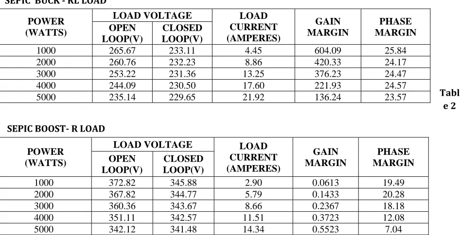
The entries in Tables 1 and 2 include the load current, output voltage and their corresponding gain and phase margins over a range of load powers. The closely regulated output voltages and the positive gain and phase margins bring out the effective role of the proposed compensating feedback technique.
Table 1
SEPIC BUCK RL LOAD
Tabl e 2
SEPIC BOOST R LOAD
POWER (WATTS)
LOAD VOLTAGE LOAD
CURRENT (AMPERES)
GAIN MARGIN
PHASE MARGIN OPEN
LOOP(V)
CLOSED LOOP(V)
1000 265.67 233.11 4.45 604.09 25.84
2000 260.76 232.23 8.86 420.33 24.17
3000 253.22 231.36 13.25 376.23 24.47
4000 244.09 230.50 17.60 221.93 24.57
5000 235.14 229.65 21.92 136.24 23.57
POWER (WATTS)
LOAD VOLTAGE LOAD
CURRENT (AMPERES)
GAIN MARGIN
PHASE MARGIN OPEN
LOOP(V)
CLOSED LOOP(V)
CONCLUSION
Thesmall signal model of the SEPIC Converter has been constructed and a suitable compensating network incorporated in order to cater to tight output voltage regulation and ensure its stability over a range of variations in load. An appropriate firing strategy required to generate the switching pulses for the lone power switch has also been part of the proposed approach. The steady state stability of the Converter has been evaluated both in time and frequency domain through Root locus and Bode plot techniques to highlight the suitability of the use of the Converter in both Buck and Boost modes for present day applications that requires precise stable dc outputs voltages over a desired range of variations in load.
REFERENCES:
1. Ekaitz Zulueta, Teodoro Rica, Jose Maria Gonzalez De Durana, “ Hybrid modeling of open loop DC – DC converters”, REVISTA Facultad De Ingenieria, U.T.A(CHILE), Vol.11, No.2, 2003, pp. 41 – 47.
2. D. Giaouris, S. Banerjee, B. Zahawi and V. Pickert, “ Stability analysis of the continuous- conduction-mode buck converter via flippov’s method”, IEEE transactions on circuits and systems – I, Vol. 55, pp. 1084 – 1096, May 2008.
3. L. Guo, J.Y. Hung, R.M. Nelms , ” PID controller modifications to improve steady state performance of digital controllers for Buck and Boost converters”, Proc. 17th Annu. IEEE Appl. Power Electron. Conf. Exp., Dallas, TX, Feb 2002, pp. 381- 388.
4. Wei Gu, “Small signal modelling for current mode controlled CUK and SEPIC converters”, IEEE PEDC 2005, pp.906–910.
5. Kavitha, P. Vishalini, G. Uma, “Analysis of stability, Bifurcation and Chaos in a SEPIC DC - DC converter”, NICE Journal of Emerging Technology, Vol.2, No.1, June 2007, pp.8-20.
6. Hao Peng, Aleksandar Prodic, “Modeling of quantization effects in digitally controlled DC-DC converters”, IEEE Transactions on Power Electronics, Vol.22, No.1, January 2007, pp.208 – 215.
7. Suzana Uran, Miro Milanovid, “State controller for Buck converter”, IEEE, EUROCON 2003, pp. 381-385.
8. G. Spiazzi, P. Mattavelli,” Design criteria for power factor pre regulators based on SEPIC and CUK converters in continuous conduction mode”, IEEE 1994, pp.1084-1089.
9. Stefan Almer, Ulf Josson, Chung- Yao Kao, and Jorge Mari, “Global Stability Analysis of DC-DC Converters Using Sampled-Data Modeling”, proceedings of the 2004 American Control Conference Boston, Massachusetta, June 30 – July 2,2004.
10. H.A. Latchman, O. D. Crisalle,Exact “Robustness Analysis for Highly Structured Frequency-Domain Uncertainties”, Proceedings of the American Control Conference, June 1996.
11. Wester, G. W. and R. D. Middlebrook, “Low-frequency characterization of switched dc-dc converters”, IEEE Transactions on Aerospace and Electronics Systems 9(3), 1972, pp. 376-385.
12. Middlebrook, R. D. and S. Cuk (1977)” A general unified approach to modeling switching converter power stages”, Proceedings of Power Electronics Specialists Conference. pp. 521-550.