FPGA Controlled Simplified H-Bridge Multilevel
Inverter
P. Suresh
Tamil Nadu Electricity Board, Vellore, Chennai, India Email: [email protected]
R. Kavin and B. Jayamanikandan
Dept. of EEE, Excel College of Engineering and Technology, Tamilnadu, India Email: {kavin882, naresh03}@gmail.com
S. Anbumani
Dept. of ECE, Excel Engineering College, Tamilnadu, India Email: [email protected]
Abstract—the multilevel inverter is recently applied in many industrial applications such as ac power supplies, static var compensators, drive system, etc. One of the significant advantages of multilevel configurations is the harmonic reduction in the output waveform without increasing switching frequency or decreasing the inverter power output. The output voltage waveform of multilevel inverter is composed of the number of levels of voltages, typically obtained from capacitor voltage sources. The so-called multivel inverter starts from three levels. As the number of level reach infinity, the output THD approaches zero. This work reports a multilevel inverter using an H-Bridge output stage with a bidirectional auxiliary switch. This Simplified H-bridge multilevel inverter produces a significant reduction of power devices and capacitor required to implement a multilevel output.
Index Terms—bidirectional auxiliary switches, field programmable gate array, h-bridge, multilevel inverter
I. INTRODUCTION
The different topologies presented in the literature as a multilevel inverter show a number of characteristics in common. The main disadvantage associated with the multilevel inverter configurations is their circuit complexity [1] requiring a high number of power switches. When we are entering the simplified H-Bridge multilevel inverter, power devices will be reduction and circuit complexity also reduction so circuit losses also reducing.
Even taking into account the technological tendency to lower the prize at which multilevel inverter can compete with standard configurations. As contribution to solve this twin Problem (cumbersome power stage and complex firing control circuit) this work proposes a new converter topology, presented [2] as a block diagram in Fig. 1(a). This topology includes an H-Bridge stage with an auxiliary
Manuscript received January 27, 2014; revised October 20, 2014.
bidirectional switch, drastically reducing the power circuit complexity, and a modulator and firing control circuit developed using a field programmable gate array (FPGA). These two Concepts used in the design of the seven level bridge converters [3] presented below. The new converter topology used in the power stage offers an important improvement in term of lower component count and reduced layout complexity, when compared with the five level converters presented in the literature [4], [5]. The simplified H-bridge multilevel inverter achieves a reduction in the number of main switch required and uses no more diodes and capacitors that the second best topology, the asymmetric cascade configurations [6]. In the modulator circuit, the FPGA can perform all required modulation functions providing another important reduction in cost and circuit complexity [7].
Figure 1(a). Block diagram of simplified h-bridge multilevel inverter
II. POWER STAGE
A. Circuit Configuration
Fig. 1(a) shows that block diagram of simplified H-bridge multilevel inverter and Fig. 1(b) shows that five level simplified H-bridge multilevel inverter. Fig. 1(c) shows that a simplified seven level H- bridge inverter. The H-bridge is formed by four main power devices, S1 to S4. For seven level output voltage [8] two auxiliary switches, four main switches and three capacitors requires.
B. Stage Advantages
To prove the reduction in component numbers achieved by this simplified H-bridge multilevel inverter configuration, Table I present the number of component required to implement [9] a seven level inverter using simplified H- bridge multilevel inverter and three previously defined ones: the two that considered as the standard multi level stages [10], the diode clamped and the capacitor clamped configuration, and a new and highly improved multi level stage, the symmetric cascade configuration [11]
The new configurations reduce the number of diodes and capacitors, when compared with diode clamped configurations. The new configurations reduce the number
of capacitors [13], when compared with the capacitor clamped configurations. The new configurations use no more diodes or capacitors that the second best topology in the table, the asymmetric cascade configurations.
Additionally, since three capacitors are connected in parallel with the main dc power supply, no significant capacitor voltage swing is produced during normal operation [14], [15] avoiding a problem that can limit operating range in some other multi level configurations.
C. Power Stage Operation
The required seven voltage output level (Vs, 2Vs/3, Vs/3, 0, -Vs/3, -2Vs/3, -Vs) are generated as follows:
1) Maximum positive output level (Vs): S1 is ON,
connecting the load positive terminal to Vs and S4 is on, connecting the load negative terminal to ground. All other control switches are OFF. The voltage applied to load terminal is Vs as in Table II
2)Positive output level (2Vs/3): The auxiliary switch S5
is ON Connecting to the load positive terminal, through
diodes D5 and D8, and S4 is ON, connecting the load negative terminal to ground. All other control switches are OFF, the voltage applied to load terminal is 2Vs/3.
3) Positive output level (Vs/3): The auxiliary switch S6 is
ON, connecting the load positive terminal, through diodes D9 and D12 and S4 is ON, connecting the load negative terminal to ground. All other control switches are OFF; the voltage applied to the load terminal is Vs/3.
4) Zero output level: The two main switches S3 and S4
are ON, short circuiting the load. All other control switches are OFF; the voltage applied to the load terminal is zero. is ON, connecting the load positive terminal, through diodes D6 and D7 and S2 is ON, connecting the load negative terminal to ground. All other control switches are OFF, the voltage applied to load terminal is -Vs/3.
6) Negative output level (-2Vs/3): The auxiliary switch
S5 is ON, connecting the load positive terminal, through diodes D10, D11 and S2 is ON, connecting the load negative terminal to ground. All other control switches are OFF, the voltage applied to load terminal is -2Vs/3.
7) Maximum negative output level (-Vs): S2 is ON,
connecting the load negative terminal and S3 is ON, connecting the load positive terminal to ground. All other control switches are OFF, load voltage applied to the load terminal is -Vs.
TABLEII. SWITCHING COMBINATIONS REQUIRED TO GENERATE THE
SEVEN-LEVEL OUTPUT VOLTAGE WAVEFORM
S1 S2 S3 S4 S5 S6 VRL
On off off On off off VS
Off off off On on off 2VS /3
Off off off On off on VS/3
Off off on On off off 0
Off on off Off off on -VS/3
Off on off Off on off -2VS /3
Off on on Off off off -VS Figure 1(c). Simplified h-bridge seven level inverter power stage
TABLE I. COMPARISON BETWEEN FOUR DIFFERENT MULTILEVEL LEVEL
INVERTERS Multilevel inverter type H-Bridge auxiliary switch Diode clamped Flying capacitor Cascaded type Main controlled switches
4 12 12 12
Auxiliary controlled switches
2 0 0 0
Diodes 12 28 12 12
Capacitor 3 8 10 2
1) Main power switches
The new topology achieves a around 40% reduction in the number of main switches required, using only six controlled power switches instead of twelve required in any of the other three configurations [12]. The auxiliary switch voltage and current rating are lower than the once required by the main controlled switches.
2) Auxiliary devices (diodes and capacitors)
III. SIMULATED RESULTS
The simplified H-bridge seven level inverter was simulated in MATLAB.
Figure 2(a). Simulated simplified h-bridge five level inverter output voltage (VDC: 100V, sample frequency is 1000Hz, the fundamental
frequency is 50Hz)
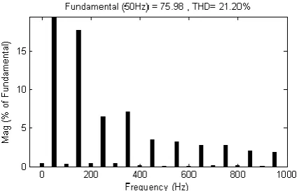
Figure 2(b). THD result for simplified h-bridge five level inverter
Figure 2(c). Simulated simplified h-bridge seven level Inverter output voltage (VDC: 300V, sample frequency is 1000Hz, the fundamental
frequency is 50Hz)
Figure 2(d). THD result for simplified h-bridge seven level inverter
IV. HARDWARE CIRCUIT DESIGN
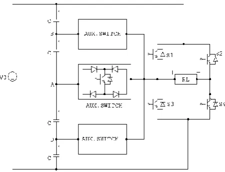
Experimental validation of the simplified H-bridge seven level inverter is going to achieve by using the configurations. Fig. 3(a) shows the simplified h-bridge Seven level inverter with RL load. Total harmonic distortion analysis is proposed seven level inverter with RL load is shown in Fig. 3(b)
Three main blocks are going to present: the modulator block, the driver circuit and the seven level inverter power stages shows in Fig. 3(c).
Figure 3(a). Simulated simplified h-bridge seven level inverter with RL load
Figure 3(b). THD result for simplified h-bridge seven level with RL load Fig. 2(a) shows that simulated output waveform for five level simplified H-bridge inverter. The sample frequency was 1000Hz amd modulation index was 0.8. It is clearly visible that the simulated output is very close to ideal output defined for five level inverter. Fundamental frequency si 50 Hz. It can be seen that the pulse duration is variable depending on the modulator previous state. The five voltage levels in the Figureure are Vs=200V, Vs/2=100V, 0V, -Vs/2=-100V, -Vs=-200V. Fig. 2(b) shows that total harmonic distortion, the percentage of THD analysis in conventional five level inverter is 21.20%.
V. CONCLUSION
A cost effective simplified H-bridge seven level inverter has been developed and simulated using MATLAB. A performance comparison of the proposed simplified seven level inverter with a conventional simplified H-bridge five level inverter is also made in terms of total Harmonic distortion (THD) response. The multi level inverter is number of level will be increasing THD approaches to zero.
A further development of the simplified H-bridge multilevel inverter able to be applied to any number of
voltage levels with in the power switches maximum The inverter power stage under study will consist of an H-bridge n-level capacitor voltage divider.
REFERENCES
[1] G. Ceglia, et al., “A new simplified multilevel inverter topology for DC-AC conversion,” IEEE Transactions on Power Electronics, vol. 21, no. 5, Sep. 2006.
[2] J. Rodriguez, J.-S. Lai, and F. Z. Peng, “Multi-Level inverter: A survey of topologies, controls, and applications,” IEEE Trans. Ind. Electron., vol. 49, no. 4, pp. 724-738, Aug. 2002.
[3] M. Marchesoni and P. Tensa, “Diode-Clamped multilevel converters: A practicable way to balance DC-link voltages,” IEEE Trans. Ind. Electron., vol. 49, no. 4, pp. 752-765, Aug. 2002. [4] Y. Chen, B. Mwinyiwiwa, Z. Wolanski, and B.-T. Ooi, “Unified
power flow controller (UPFC) based on chopper stabilized diode-clamped multilevel converters,” IEEE Trans. Power Electron., vol. 15, no. 2, pp. 258-267, Mar. 2000.
[5] G. Venkataramanan and A. Bendre, “Reciprocity-Transpositions-Based sinusoidal pulsewidth modulation for diode-clamped multilevel converters,” IEEE Trans. Ind. Electron., vol. 49, no. 5, pp. 1035-1047, Oct. 2002. [6] S. Sirisukprasert, J.-S. Lai, and T.-H. Liu, “Optimum harmonic
reduction with a wide range of modulation indexes for multilevel converters,” IEEE Trans. Ind. Electron., vol. 49, no. 4, pp. 87-881, Aug. 2002.
[7] L. M. Tolbert and T. G. Habertler, “Novel multilevel inverter carrier-based PWM method,” IEEE Trans. Ind. Appl., vol. 35, no. 5, pp. 1098-1107, 1999.
[8] X. Yuan and I. Barbi, “A new diode clamping multilevel inverter,”
IEEE Trans. Power Electron., vol. 15, no. 4, pp. 711-718, Jul. 2000.
[9] M. D. Majrekar, P. K. Steimer, and T. A. Lipo, “Hybrid multilevel power conversion system: A competitive solution for high-power applications,” IEEE Trans. Ind. Appl., vol. 36, no. 3, pp. 834-841, 2000.
[10] L. M. Tobert, F. Z. Peng, T. Cunnyngham, and J. N. Chiasson, “Charge balance control schemes for cascade multi-level converter in hybrid electric vehicles,” IEEE Trans. Ind. Electron., vol. 49, no. 5, pp. 1058-1064, Oct. 2002.
[11] N. P. Schibli, T. Nguyen, and A. C. Rufer, “A three-phase multilevel converter for high-power induction motors,” IEEE Trans. Power. Electron., vol. 13, no. 5, pp. 978-986, Sep. 1998.
[12] F. Z. Peng, J. W. McKeever, and D. J. Adams, “A power line conditioner using cascade multi-level inverters for distribution systems,” IEEE Trans. Ind. Appl., vol. 34, no. 6, pp. 1293-1298, 1998.
[13] S. Bernet, “Recent developments for high power converter for industry and traction applications,” IEEE Trans. Power Electron., vol. 15, no. 6 pp. 1102-1117, Nov. 2000.
[14] Nagel, S. Bernet, and P. K. Steimer, “A 24 MVA inverter using IGCT series connection for medium voltage applications,” in Proc. IEEE IAS Annu. Meeting, Chicago, IL, Oct. 2001, vol. 2, pp. 867-870.
[15] J. Bueno, R. Garcia, M. Marrón, and F. Espinosa, “Modulation techniques comparison for three levels VSI converters,” in Proc. IEEE 28th Annu. Conf. Ind. Electron. Soc., Nov. 2002, vol. 2, pp. 908-913.
Figure 3(c). Simplified h-bridge seven level hardware circuit diagram
A. Control Circuit
In the seven level inverter controls circuit generates the control signal for all the power components in the power stage. In this implementation, going to use a FPGA programmable circuit (sparton 3). All programs are going to done verilog hardware description language.
B. Interface Circuit
The interface circuit going to provide the required isolation and power gain between the modulator seven output and power devices gate.
C. Power Stage
The power stage going to assemble by using IGBT H-bridge with auxiliary switch module. The auxiliary is containing diodes and IGBT.
Figure 4. Generalized multilevel inverter configurations using the simplified h-bridge
voltage, is now under consideration. As shown in Fig. 4.
R. Kavin was born in the year of 1985, at komarapalayam. He did B.E (EEE) at KSR College of technology in the year of 2007. He did his M.E (PED) at Sri Venkateswara college of Engineering in the year of 2010, Sriperumpudhur, Chennai, Tamilnadu, India, Currently he is working as Assistant Professor in the Dept. of EEE at Excel College of Engineering & Technology, Komarapalayam, Namakkal District, Tamilnadu, India.
S. Anbumani was born in the year of 1989, at Bhavani. She did B.E (BME) at Vellalar College of Engineering & technology in the year of 2010. She did her M.E (Applied Electronics) at SSM college of Engineering in the year of 2012. Currently she is working as Assistant Professor in the Dept. of ECE at Excel Engineering College, Komarapalayam, Namakkal District, Tamilnadu, India.
B. Jayamanikandan was born in Erode on April 3, 1986. He was graduated in 2007 from Sri Ramakrishna Institute of Technology, Coimbatore and post graduated in 2012 at Anna University of technology, Coimbatore. He is currently working as Assistant Professor in the department of EEE at Excel College of Engineering and Technology, Komarapalayam from June 2012. He has published papers in more than 5 International journals. He also presented papers in more than 20 Conferences. His research interests involve in power electronics, renewable energy power generation.