Volume 2006, Article ID 57134, Pages1–18 DOI 10.1155/ASP/2006/57134
An Efficient Circulant MIMO Equalizer for CDMA Downlink:
Algorithm and VLSI Architecture
Yuanbin Guo,1Jianzhong(Charlie) Zhang,1Dennis McCain,1and Joseph R. Cavallaro2
1Nokia Research Center, 6000 Connections Drive, Irving, TX 75039, USA
2Department of Electrical and Computer Engineering, George R. Brown School of Engineering,
Rice University, 6100 Main Street, Houston, TX 77005, USA
Received 29 November 2004; Revised 5 June 2005; Accepted 14 June 2005
We present an efficient circulant approximation-based MIMO equalizer architecture for the CDMA downlink. This reduces the direct matrix inverse (DMI) of size (NF×NF) withO((NF)3) complexity to some FFT operations withO(NFlog
2(F)) complexity and the inverse of some (N×N) submatrices. We then propose parallel and pipelined VLSI architectures with Hermitian optimiza-tion and reduced-state FFT for further complexity optimizaoptimiza-tion. Generic VLSI architectures are derived for the (4×4) high-order receiver from partitioned (2×2) submatrices. This leads to more parallel VLSI design with 3×further complexity reduction. Comparative study with both the conjugate-gradient and DMI algorithms shows very promising performance/complexity trade-off. VLSI design space in terms of area/time efficiency is explored extensively for layered parallelism and pipelining with a Catapult C high-level-synthesis methodology.
Copyright © 2006 Hindawi Publishing Corporation. All rights reserved.
1. INTRODUCTION
Wireless communication is experiencing radical advance-ment to support broadband multimedia services and ubiqui-tous networking via mobile devices. MIMO (multiple-input multiple-output) technology [1–3] using multiple antennas at both the transmitter and receiver has emerged as one of the most significant technical breakthroughs for throughput
en-hancement. On the other hand, UMTS [4] and CDMA2000
extensions optimized for data services lead to the standard-ization of multicode CDMA systems such as the high-speed downlink packet access (HSDPA) and its equivalent 1X evo-lution data and voice/data optimized (EV-DV/DO) stan-dards [5]. This leads to an asymmetric capacity requirement, where the downlink even plays a more essential role than the uplink because of the downloading features. The application of the MIMO technology in CDMA downlink receives in-creasing interest as a strong candidate for the 3G and beyond wireless communication systems.
Known as D-BLAST [3] and a more realistic strategy as V-BLAST [2] for real-time implementation, the orig-inal MIMO spatial multiplexing was proposed for nar-rowband and flat fading channels. In a multipath fading channel, the orthogonality of the spreading codes is de-stroyed. This introduces both the multiple-access interfer-ence (MAI) and the intersymbol interferinterfer-ence (ISI). The con-ventional Rake receiver [6] could not provide acceptable
per-formance because of the very short spreading gain to sup-port high-rate data services in multicode CDMA downlink. LMMSE (linear-minimum-mean-squared-error)-based chip equalizer is promising to restore the orthogonality of the spreading code and suppress both the ISI and MAI [6] in single-antenna systems. However, this involves the inverse of a large covariance matrix withO((NF)3) complexity for MIMO systems, whereNis the number of receive antennas andF is the channel length. Traditionally, the implementa-tion of equalizer in hardware has been one of the most com-plex tasks for receiver designs. The MIMO extension gives even more challenges for real-time hardware implementation [7], especially for the mobile receiver.
In this paper, we first present an FFT-based fast algorithm for the tap solving by approximating the block Toeplitz struc-ture of the covariance matrix with a block-circulant matrix to avoid the direct matrix inverse. The inverse of the large co-variance matrix is reduced to some parallel FFT/IFFT opera-tions and the inverse of some much smaller submatrices. This algorithm reduces the complexity order to O(NFlog2(F)), which makes the real-time implementation much easier. An algorithmic-level comparative study for different equaliz-ers demonstrates their promising performance/complexity tradeoff.
As real-time implementation is concerned, system-on-chip (SoC) architecture offers more parallelism, more com-pact size, and lower power consumption than general pur-pose DSP processors. However, the research for the SoC architectures of MIMO-HSDPA mobile receiver remains a relatively new and hot topic. Recently, Nokia success-fully demonstrated a single-antenna HSDPA real-time sys-tem in the CTIA’03 wireless trade show [13,14]. Although MIMO-VLSI implementations have been reported for
Lu-cent’s BLAST ASIC chip [15] and some MIMO detection
algorithms [16], the VLSI architecture design of MIMO-CDMA equalizers remains a new research topic. To support the MIMO-CDMA downlink in a multipath fading channel, it is necessary to explore the efficient VLSI design architec-ture [17] for the complex equalizer.
In the second part, we focus on the VLSI-oriented op-timizations of the architecture complexity. Hermitian opti-mization is proposed by utilizing the structures of the cor-relation coefficients and the FFT algorithm. A reduced-state FFT module is proposed to avoid redundant computation of the symmetric coefficients and the zero coefficients. This reduces both the number and complexity of the conven-tional FFT module. On the other hand, the matrix inverse of some smaller submatrices of size (N ×N) is inevitable for the MIMO receiver although the (NF ×NF) inverse is avoided. For a high-order MIMO receiver, the complex-ity still increases dramatically with the number of antennas. Therefore, the Hermitian feature is applied to reduce the sub-matrix inverse complexity. Of particular interest is the non-trivial (4×4) MIMO configuration. We apply a divide-and-conquer method to partition the (4×4) submatrices into four (2×2) submatrices. The (4×4) matrix inverse is then dra-matically simplified by exploring the commonality in a parti-tioned matrix inverse lemma. Generic VLSI architectures are derived from the special design blocks to eliminate the re-dundancies in the complex operations. The regulated model facilitates the design of efficient parallel VLSI modules such
as “complex-Hermitian-multiplication,” “Hermitian inverse”
and “diagonal transform.” This leads to efficient architectures with 3×further complexity reduction and more parallel and pipelined schematic.
In addition to minimizing the circuit area used, the de-sign needs to work within a time budget. There are many area/time tradeoffs in the VLSI architectures. Extensive ar-chitecture tradeoffstudy provides critical insights into im-plementation issues that may arise during the product de-velopment process. However, this type of SoC design space
exploration is extremely time consuming because the stan-dard trial-and-optimize approaches today are usually tied to hand-coded VHDL/Verilog-based methodology [18,19]. In this paper, we present a Catapult C-based [13] high-level-synthesis (HLS) methodology which integrates several key technologies to explore the VLSI architecture tradeoffs ex-tensively. Extensive design space exploration is enabled by al-locating different architecture/resource constraints in a Cat-apult C architecture scheduler [13]. Synthesizable register-transfer-level (RTL) design is generated from an algorithmic C/C++ fixed-point design, integrated in other downstream flows and validated in a Xilinx FPGA prototyping platform.
The rest of the paper is organized as follows.Section 2
gives the MIMO-CDMA downlink system model. The FFT-based circulant chip equalizer is presented in Section 3.
Section 4 presents the system-level partitioning and the VLSI-level complexity optimization. The comparative per-formance and complexity analysis are presented inSection 5. Finally,Section 6presents the HLS-based design space explo-ration and an experimental implementation on FPGA.
2. SYSTEM MODEL FOR MIMO-CDMA DOWNLINK
The system model of the MIMO multicode CDMA down-link withMTx antennas andNRx antennas is described in
Figure 1. In a multicode CDMA downlink, multiple spread-ing codes are assigned to a sspread-ingle user to achieve high data rate. By using spatial multiplexing, the high data rate symbols are demultiplexed intoKM lower-rate substreams, whereK
is the number of spreading codes for data transmission. The substreams are divided intoMgroups, where each substream in the group is spreaded with a spreading code of spreading gainG. Each group is then combined and scrambled with long scrambling codes and transmitted through themth Tx antenna. The chip-level signal at themth transmit antenna is given bydm(i+j∗G)=
K
k=1skm(j)cmk(i) +sPm(j)cmP(i), where
jis the symbol index,iis the chip index, andkis the index of the composite spreading code.sk
m(j) is thejth symbol of the
kth code at themth substream. In the following, we focus on thejth symbol and omit the symbol index for notation sim-plicity.ck
m(i) = ck(i)c(ms)(i) is the composite spreading code
sequence for thekth code at themth substream, whereck(i)
is the user-specific Hadamard code andc(ms)(i) is the
antenna-specific scrambling long code.sP
m(j) denotes the pilot
sym-bols at themth antenna.cP
m(i)=cP(i)c
(s)
m(i) is the composite
spreading code for pilot symbols at themth antenna. The re-ceived chip-level signal at thenth Rx antenna is given by
rn(i)= M
m=1
Lm,n
l=0
hm,n(l)dm
i−τl
+zn(i), (1)
wherehm,n(l) andLm,n are thelth path channel coefficient
and the delay spread between themth Tx antenna and the
nth Rx antenna, respectively. zn(i) is the additive Gaussian
noise at thenth receive antenna.
By packing the received chips from all the receive anten-nas in a vectorr(i)=[r1(i),. . .,rn(i),. . .,rN(i)]Tand
c1(i)
ck(i) Spreader
Spreader
Pilot 1
Scrambling
S1,1(i)
S1,k(i)
c1(i)
ck(i) Spreader
Spreader PilotM
Scrambling
SM,1(i)
SM,k(i) High-speed
bit stream
b(t) TX
DEMUX
d1(i)
dM(i) h1,1
hM,N
r1(i)
rN(i)
Downlink receiver .
. .
. . .
. . .
. . .
Figure1: The system model of the MIMO multicode CDMA downlink.
chip from all theN Rx antennas, we form a signal vector as
rA=[r(i+F)T,. . .,r(i)T,. . .,r(i−F)T]T. Here,Fis the
obser-vation window length corresponding to the channel length. In the vector form, the received signal can be given by
rA(i)= M
m=1
Hmdm(i), (2)
whereHm is a block Toeplitz matrix constructed from the
channel coefficients as shown in [20]. The multiple receive antennas’ channel vector is defined as hm(l) = [hm,1(l),
. . .,hm,n(l),. . .,hm,N(l)]T. The transmitted chip vector for
the mth transmit antenna is given by dm(i) = [dm(i +
F),. . .,dm(i),. . .,dm(i−F−L)]T.
3. LMMSE TAP SOLVER WITH CIRCULANT APPROXIMATION
3.1. LMMSE chip equalizer
LMMSE chip-level equalization has been one of the most promising receivers in the single-user CDMA downlink. Chip equalizer estimates the transmitted chip samples by a set of linear FIR filter coefficientswH
m(i) to restore the code
orthogonality as
dm(i)=wHm(i)rA(i). (3)
It is well known that the LMMSE chip equalizer coefficients are given by minimizing the MSE between the transmitted and recovered chip samples as
woptm (i)=arg min
wm(i)
Edm(i)−wHm(i)rA(i)2
=σd2(i)Rrr(i)−1hm(i),
(4)
whereσ2
d(i) is the transmitted chip power.Rrr(i) andhm(i)
are the covariance estimation and channel estimation, re-spectively. Here, the covariance matrix is estimated by the time-average with ergodicity assumption as
Rrr(i)=E
rA(i)rHA(i)
= 1
NB NB−1
i=0
rA(i)rHA(i), (5)
whereNBis the length for the time average. The channel
co-efficients are estimated ashm(i) = E[rA(i)dHm(i)] using the
pilot symbols. In the HSDPA standard, about 10% of the to-tal transmit power is dedicated to the common pilot chan-nel (CPICH). This will provide accurate chanchan-nel estimation. By assuming that the channel is stationary over the observa-tion window length, we can have a block-based operaobserva-tion by omitting the chip index inRrr(i),hm(i), andwm(i).
3.2. FFT-based circulant approximation tap solver
Using the stationarity of the channel and the convolution property, it is easy to show that the covariance matrix is a banded block Toeplitz matrix as
Rrr=
⎛ ⎜ ⎜ ⎜ ⎜ ⎜ ⎜ ⎜ ⎜ ⎜ ⎝
E[0] · · · EH[L] · · · 0
..
. . .. . .. · · · ...
E[L] . .. . .. · · · EH[L]
..
. . .. · · · ... . ..
0 · · · E[L] · · · E[0]
⎞ ⎟ ⎟ ⎟ ⎟ ⎟ ⎟ ⎟ ⎟ ⎟ ⎠
, (6)
where E[l] is an (N × N) block matrix with the cross-antenna covariance coefficients. The dimension of the ma-trix is (NLF×NLF), whereLFis determined by the channel
The direct inverse of the matrix is very expensive for hard-ware implementation.
To reduce the computation complexity, an FFT-based fast algorithm is presented in this section. It is known that a cir-culant matrix Scan be diagonalized by the FFT operation as S = DHΛD, whereD is the FFT phase coefficient
ma-trix andΛis a diagonal matrix whose diagonal elements are the FFT result of the first column of the circulant matrixS. This known lemma is applied to simplify the MIMO equal-izer computation dramatically. It is shown that the covari-ance matrixRrr can be approximated by a block-circulant
matrix after we add two corner matrices as
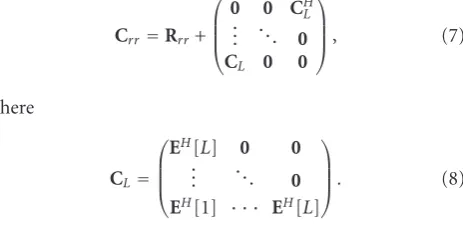
Crr=Rrr+
⎛ ⎜ ⎜ ⎝
0 0 CH L
..
. . .. 0 CL 0 0
⎞ ⎟ ⎟
⎠, (7)
where
CL=
⎛ ⎜ ⎜ ⎝
EH[L] 0 0
..
. . .. 0
EH[1] · · · EH[L]
⎞ ⎟ ⎟
⎠. (8)
Using the extension of the diagonalization lemma and the features ofKroneckerproduct, the block-circulant matrix can be decomposed as
Crr=
DH⊗I
LF−1
i=0
Wi⊗E[i]
D⊗I, (9)
whereW= diag(1,W−1
LF · · ·W
−(LF−1)
LF ) andWLF =ej(2π/LF) is the phase factor coefficient for the DFT computation. denotes theKroneckerproduct. By denoting
F= LF−1
i=0
Wi⊗E[i]
, (10)
it can be shown that the final MIMO equalizer taps are com-puted as the following equation:
woptm ≈DH⊗I·F−1·(D⊗I)hm. (11)
F = diag(F[0],F[1],. . .,F[LF]) is a block-diagonal matrix
with elements taken from the element-wise FFT of the first column of the block-circular matrix Crr. For an (M ×N)
MIMO system, this reduces the inverse of an (NLF×NLF)
matrix to the inverse of subblock matrices with size (N×N).
3.3. System-on-chip (SoC) architecture partitioning
To achieve the real-time implementation, either DSP pro-cessors or VLSI architectures could be applied. For exam-ple, a multiple-processor architecture using TI’s DSP proces-sors has been reported in [21] for the 3G base station im-plementation. However, the requirement for low power con-sumption and compact size makes it difficult to use multiple DSPs in a mobile handset to achieve the real-time processing
power for the chip-level physical layer design, especially for the MIMO systems. SoC architecture is a major revolution for integrated circuits due to the unprecedented levels of integration and many advantages on the power consump-tion and compact size. However, the straightforward imple-mentation of the proposed equalizer has many redundancies in computation. Many optimizations are needed to make it more suitable for real-time implementation. We emphasize the interaction between architecture, system partitioning, and pipelining in this section with these objectives: (1) pro-pose VLSI-oriented optimizations to further reduce the com-putation complexity; (2) implement the equalizer with the minimum hardware resource to meet the real-time require-ment; (3) obtain an efficient architecture with optimal par-allelism and pipelining for the critical computation parts. To explore the efficient architectures, we elaborate the tasks as the following procedure.
(1) Compute the independent correlation elements [E[0],
. . .,E[L]], and form the first block column of circu-lant C(1)rr by adding the corner elements as C(1)rr =
[E[0],. . .,E[L],0,. . .,0,EH[L],. . .,EH[1]]T. Each
ele-ment is an (N×N) subblock matrix.
(2) Take the element-wise FFT ofC(1)rr, where the element
vectorsFn1,n2=FFT{E
(c)
n1,n2}andE
(c)
n1,n2(i)=C
(1)
rr [(n1−
i−1)∗N+n2−1] fori∈[0,LF],n1,n2∈[1,N].
(3) For m ∈ [1,M] and n ∈ [1,N], compute the
dimension-wise FFT of the channel estimation as
Φm=(D⊗I)hm=FFT([0,. . ., 0,hm,n(L),. . .,hm,n(0),
0,. . ., 0]).
(4) Compute the inverse of the block-diagonal matrixF, whereF−1=diag(F[0]−1,. . .,F[L
F−1]−1) andF[i] is
an (N×N) submatrix formed from theith subcarrier ofFn1,n2.
(5) Compute the matrix multiplication of the submatrices inverse with the FFT output of channel estimation co-efficientsΨm=F−1Φm.
(6) Compute the dimension-wise IFFT of the multiplica-tion resultswoptm ≈(DH⊗I)Ψm.
With a timing- and data-dependency analysis, the top-level block diagram for the MIMO equalizer is shown in
Figure 2. The system-level pipeline is designed for bet-ter modularity. In the front end, a correlation estimation block takes the multiple-input samples for each chip to compute the covariance coefficients of the first column of
Rrr. It is made circulant by adding corner to form the
matrix [E[0],. . .,E[L],0,. . .,0,E[L]H,. . .,E[1]H]. The
com-plete coefficients are written to DPRAMs and the (N×N) element-wise FFT module computes [F[0],. . .,F[LF]] =
FFT{E[0],. . .,E[L],0,. . .,0,E[L]H,. . .,E[1]H}.
Another parallel data path is for the channel estimation and the (M×N) dimension-wise FFTs on the channel coef-ficient vectors as in (D⊗I)hm. A submatrix inverse and
mul-tiplication block takes the FFT coefficients of both the chan-nel estimation and correlation estimation coefficients from DPRAMs and carries out the computation as inF−1Φ
m.
N×NMIMO correlation E[0],. . .,E[L]
S/P & form
R DPRAM
N×N
MIMO FFT DPRAM
N×N
submatrix inverse
& multiply
DPRAM
M×N
MIMO IFFT
M×NMIMO channel estimation h[0],. . .,h[L]
Form H
DPRAM
N×N
MIMO FFT DPRAM
DPRAM
w[0], . . . , w[LF−1] S/P % load FIR coefficients
M×NMIMO FIR Pilot
symbols d[i] Streaming
datar[i]
Figure2: The block diagram of the VLSI architecture of the FFT-based MIMO equalizer.
(M×N) MIMO-FIR block for filtering. To reflect the cor-rect timing, the correlation and channel estimation mod-ules at the front end will work in a throughput mode on the streaming input samples. The FFT-inverse-IFFT modules in the dotted line block construct the postprocessing of the tap solver. They are suitable to work in a block mode us-ing dual-port RAM blocks as interface between blocks. The MIMO-FIR filtering will also work in throughput mode on the buffered streaming input data.
4. VLSI-LEVEL COMPLEXITY OPTIMIZATION
4.1. Hermitian optimization
In this section, more emphasis is given to the VLSI-oriented implementation aspects. For QPSK and QAM modulation schemes, all the numerical computations in the algorithm are associated with complex numbers. However, the complexity in the hardware is reflected by the number of real multipli-cations, additions, and divisions, and so forth. It is more ac-curate to clarify the complexity for different types of com-putations. For example, a general “complex (a)×complex
(b)” numerical computation has 4 real multiplications and 2 real additions, but a “complex (a)×conjugate(a)” reduces to only 2 real multiplications and 1 real addition. By defin-ingFn1,n2[0 :LF−1] as the element-wise FFT vector of the
covariance block-vector forn1,n2∈[1,N], we show that the element-wise FFT of the circulant covariance vectors admits a Hermitian structure. This leads to the following lemmas for complexity reduction.
Lemma 1 (Hermitian). Fn1,n2=conj(Fn2,n1), where the vector is formed from the covariance element vector between antennas
n1andn2.Fn2,n1is redundant forn2< n1.
Lemma 2 (Hermitian complexity). The computation of
Fn1,n1can be reduced to onlyL/LFof the full DFT module.
Proof. For the Rx antennasn1,n2, it can be shown that the
el-ements in the circulant column have the following relations, whereNBis the covariance time-average window length:
E(c)
n1,n2(0)=
E(c)
n2,n1(0)
∗=NB−1
i=0
rn1(i)rn2(i)
∗,
E(nc1),n2(l)=
E(nc2),n1
LF−l
∗
=
NB−1
i=0
rn1(i)rn2(i+l)
∗,
E(c)
n1,n2
LF−l
=E(c)
n2,n1(l)
∗=NB−1
i=0
rn2(i)rn1(i+l)∗,
E(c)
n1,n2(l)=
E(c)
n2,n1
LF−l
∗
=0 otherwise.
(12)
Using the features of the FFT, it can be proven that the element-wise FFT results have the relation thatFn1,n2 =
(Fn2,n1)∗. The submatrix formed by theith entry of Fn1,n2
is an (N × N) Hermitian symmetric matrix as F(i) =
(Fn1,n2(i))N×N =F(i)H.
Thus, instead of havingN×Ncomplex FFT
computa-tions, we only need to compute the element-wise FFT for the lower triangle matrix. The number of FFTs in the element-wise FFT is reduced fromN2 to (N2+N)/2. Moreover, the element-wise FFT coefficients of the diagonal elements are all real numbers. This leads to the design of the reduced-state MIMO-FFT blocks.
4.2. Reduced-state FFT
Stage 1 Stage 2 Stage 3 Stage 4
x(0)=0
x(8)=0
x(4)
x(12)=0
x(2)
x(10)=0
x(6)=0
x(14)=0
x(1)
x(9)=0
x(5)=0
x(13)=0
x(3)
x(11)=0
x(7)=0
x(15)=0
0 0
x(4)
x(4)
W40
W1 4
x(2)
x(2) 0 0
x(1)
x(1) 0 0
x(3)
x(3) 0 0
x(2)
x(2)
x(2)
x(2)
W0 8
W1 8
W2 8
W3
8 −1
−1
x(1)
x(1)
x(1)
x(1)
W0 16
W1 16
W162
W3 16
W4 16
W5 16
W6 16
W167
x(3)
x(3)
x(3)
x(3)
W0 8
W1 8
W2 8
W3 8
−1 −1
Figure3: Reduced-state FFT butterfly tree.
unit, each operation involves a full complex multiplication, which has 4 real multiplications and 2 real additions. Since thekth subcarrier of theFmmvector is
fmm(k)=emm(0) + 2
L
i=1
emm(i)WL−Fki
, (13)
by defining the input sequence to the FFT module as{x(i)} =
[0,emm(1),. . .,em,m(L), 0,. . ., 0], we only need to compute
the real part FFT of the x(i) to get fmm(k). From the
but-terfly decomposition, we have the recursion for the real-part FFT computation as
X(k)= X1(k)
+Wk
LFX2(k)
,
X
k+LF 2
= X1(k)
− Wk LFX2(k)
(14)
fork =0, 1,. . .,LF/2−1. This reduces the complex
multi-plication and addition to only real multimulti-plication and addi-tion for one stage. The butterfly unit becomes a reduced-state partial-butterfly-unit (PBFU) as the dotted line units shown inFigure 3for an example of 16-point FFT.
From the recursion, it can be shown that we can prune the redundant computations by replacing the complex mul-tiplication in the butterfly units for some portion of the FFT BFU tree. Before considering the many zeros in the input
Table1: Complexity comparison for different FFT schemes.
Real mult Real add Full FFT 2LFlog2LF LFlog2LF RS-FFT w/o ZP 2Nlog2LF−2LF+ 2 LFlog2LF−2LF+ 2 RS-FFT with ZP 2LFlog2LF−6LF+ 12 LFlog2LF−4LF+ 12
coefficients, the total number of PBFU isLF−1. Since the
total number of BFU is (LF/2) log2LF, the total number of
full-BFU (FBFU) is given by (LF/2) log2LF−LF+ 1.
Con-sidering thatx(i)=0 only fori ∈[1,L],L < LF/2, we can
further truncate the computations related to the zero values. After pruning all the unnecessary BFU branches, the FBFUs and PBFUs only take effects from stage 3. The number of FBFU is reduced to (LF/2)∗log2LF−2LF+ 6. This also
saves roughly 50% of the real multiplications because the FFT length within 64 points will suffice for most realistic equalizer applications.
4.3. Hermitian matrix inverse architectures
In this section, we utilize the Hermitian feature and focus on the optimization of the submatrix inverse and multiplication module following the element-wise FFT modules in the tap solver. Although the FFT-based tap solver avoids the direct matrix inverse of the original covariance matrix with the di-mension of (NF×NF), the inverse of the diagonal matrix
Fis inevitable. For a MIMO receiver with high receive di-mension, the matrix inverse and multiplication inF−1h
mis
not trivial. BecauseFis a block-diagonal matrix, its inverse can be decomposed to the inverse ofLF submatrices of size
(N×N) as in
F−1=diagF[0]−1,F[1]−1,. . .,FLF−1
−1
. (15)
A traditional (N×N) matrix inverse using Gaussian elim-ination has the complexity at O(N3) complex operations. Cholesky decomposition can be applied to facilitate the in-verse of these matrices. However, this method requires arith-metic square root operation, which is expensive for hardware implementation. Considering the fact that it is unlikely to have more than four Rx antennas in a mobile terminal, we consider the two special cases individually, that is, 2 and 4 Rx antennas. We propose complexity-reduction schemes and ef-ficient architectures suitable for VLSI implementation based on the exploration of block partitioning. The commonality of the partitioned block matrix inverse is extracted to design generic RTL modules for reusable modularity. We then build the (4×4) receiver by reusing the (2×2) block partitioning.
4.3.1. Dual-antenna MIMO receiver
From (11), a straightforward partitioning is at the matrix inversion of F and then the matrix multiplication of the dimension-wise FFT of the channel coefficients asF−1(D⊗ I)hm. In this partitioning, we would first compute the inverse
of the entire subblock matrix inFand then carry out a ma-trix multiplication. However, this partitioning involves two separate loop structures. In the VLSI circuit design, this will introduce some overhead for memory access and finite-state machine logic. Since the two steps have the same loop struc-ture, it is more desirable to merge the two steps and reduce the overhead shown as follows. The inverse of a (2×2) sub-matrix is given by
F[k]−1=
f00(k) f01(k)
f10(k) f11(k)
−1
= 1
f00(k)f11(k)−f01(k)f10(k)
f11(k) −f01(k)
−f10(k) f00(k)
.
(16)
Let Γ = (D ⊗I)hm = [Γ[0],Γ[1],. . .,Γ[LF−1]], where
Γ[k]=[e1(k)e2(k)] is the combination of thekth elements
of the dimension-wise FFT coefficients, then a merged com-putation of the matrix inverse and multiplication is given by
W=F−1·(D⊗I)h
m
=diagF[0]−1,F[1]−1,. . .,FLF−1
−1
Γ =F[0]−1Γ[0]T,F[1]−1Γ[1]T,. . .,FL
F−1
−1
ΓLF−1
T
.
(17)
Thus, we can use a single merged loop to compute the final result ofWinstead of using separate loops. Moreover, with theHermitianfeatures ofF00andF11, we can reduce the number of real operations in the matrix inverse and multi-plication module. This leads to a simplified equation for the
kth element of the matrixWas
W(k)= 1
f00(k)·f11(k)−f01(k) 2
·
f11(k)◦e1(k)−f01(k)∗e2(k)
−f10(k)◦e2(k)−f01(k)∗e1(k)
,
(18)
where “a·b,” “a◦b,” and “a∗b” indicate a “real×real,” “real×complex” and “complex×complex” multiplication, respectively. The complex division is replaced by a real divi-sion. From this, we derived the simplified data path with the Hermitian optimization as inFigure 4. In this figure, f00(k) and f11(k) are real numbers. The single multiplier means a real multiplication. The multiplier with a circle means the “real×complex” multiplication and the multiplier with a rectangle is a “complex×complex” multiplication. The sim-plified data path facilitates the scaling, and thus increases the stability in the fixed-point implementation.
4.3.2. Receiver with 4 Rx antennas
The principle operation of interest is the inverse of the (4×4) submatrices. To achieve a scalable design, we first partition the (4×4) submatrices inF[i] into four (2×2) block sub matrices as
F(i)4×4=
⎛ ⎜ ⎜ ⎜ ⎜ ⎝
f11(i) f12(i) f13(i) f14(i)
f21(i) f22(i) f23(i) f24(i)
f31(i) f32(i) f33(i) f34(i)
f41(i) f42(i) f43(i) f44(i)
⎞ ⎟ ⎟ ⎟ ⎟ ⎠
=
B11(i) B12(i) B21(i) B22(i)
.
(19)
The inverse of the (4×4) matrix can be carried out by a se-quential inverse of four (2×2) submatrices. We also partition the inverse of the (4×4) element matrix as
F(i)−1=
C11(i) C12(i) C21(i) C22(i)
f00(k)
f01(k)
f11(k)
e2(k)
e1(k)
2
conj
−1
−1
−1
1/x
W1(k)
W2(k)
Figure4: The merged 2×2 inverse and multiplication.
B11
B12
B21
B22
[o]−1 B−111
[·]×[·] B−1
11 B12
[·]×[·]
B21B−111 B12
[·]×[·]
B21B−111B12
[·]−[·] [o]−1 C22
[·]×[·] C 21 [·]×[·]
C12 [·]×[·]
[·]−[·] C11
Figure5: The data path of the partitioned 4×4 matrix inverse for each subcarrier.
It can be shown that the subblocks are given by the following equations from the matrix inverse lemma [22]:
C22(i)=
B22(i)−B21(i)B11(i)−1B12(i)
−1 ,
C12(i)= −B11(i)−1B12(i)C22(i), C21(i)= −C22(i)B21(i)B11(i)−1,
C11(i)=B11(i)−1−C12(i)B21(i)B11(i)−1.
(21)
Without looking into the data dependency, a straightfor-ward computation will have 8 complex matrix multiplica-tions, 2 complex matrix inverses, and 2 complex matrix sub-tractions, all of the size (2×2). By examining the data de-pendency, we will find some duplicate operations in the data path. For a general case before considering the Hermitian structure of theF[i] matrix, a sequential computation has the data-dependency path given byFigure 5. The raw complex-ity is given by 6 matrix mult, 2 inverses, and 2 substractions. From the data path flow, the critical path can be identified.
Now we utilize the Hermitian feature of the F matrix to derive more parallel computing architecture. Because the inverse of a Hermitian matrix is Hermitian, that is, F−1 = [F−1]H, it can be shown that
B−1 11(i)=
B−1
11(i)
H
=⇒C11(i)=
C11(i)
H
,
B12(i)=
B21(i)
H
=⇒C12(i)=
C21(i)
H
,
B22(i)=
B22(i)
H
=⇒C22(i)=
C22(i)
H
.
(22)
This leads to the data path by removing the duplicate compu-tation blocks that has the Hermitian relationship. However, this straightforward treatment still does not lead to the most efficient computing architecture. The data path is still con-structed with a very long dependency path. To fully extract the commonality and regulate the design blocks in VLSI, we define the following special operators on the (2×2) matrices for the different complex operations. These special operators are mapped to VLSI processing units to deal with the special Hermitian matrix.
Definition 1(pseudo-power). pPow(a,b) = (a)· (b) +
(a)· (b) is defined as thepseudo-power function of two complex numbers and(a,b)= (a)· (b)− (a)· (b) is defined as the real part of a complex multiplication.
Definition 2(complex-hermitian-mult). For a general (2×2)
matrixAand a Hermitian (2×2) matrixB=BH, we define
the operator CHM (Complex-Hermitian-mult) as
M(A,B)=AB=
a11 a12
a21 a22
b11 b∗21
b21 b22
. (23)
Note that all the numbers are complex except{b11,b22} ∈R.
Definition 3 (Hermitian inverse). For a (2×2) Hermitian
defined as
HInv(B)= 1
b11b22−b212
b22 −b∗21
−b21 b11
, (24)
where there are only real multiplications and divisions.
Definition 4 (diagonal transform). Given the (4×4)
Her-mitian matrixAwhich is partitioned into four subblocks as
A=A11 AH21 A21 A22
=AH, the DT(diagonal transform)ofAis
de-fined as
T(A)=TA11,A21,A22
=A22−A21A11A21H
=A22−M
A21,A11
AH21.
(25)
With these definitions, we regulate the inverse of the (4×4) Hermitian matrixF=FHinto simplified operations
on (2×2) matrices. After some manipulation, the partitioned subblock computation equations can be mapped to the fol-lowing procedure using the defined operators:
Binv=HInv
B11
=BHinv; D=MB21,Binv
;
C22=HInv
TBinv,B21,B22
;
C12= −M
DH,C
22
;
C11=Binv+DHC22D=T
−C22,DH,Binv
.
(26)
The overall computation complexity is reduced to 2 HInv operations, 2 DTs, 1 extra CHM block. Because the sign in-verter and the Hermitian formatter [·]H have no hardware
resource at all, the computation complexity is determined by these three generic blocks. The data path of the computation shows the timing relationship between different design mod-ules. This regulated procedure facilitates the design of effi -cient parallel VLSI modules, whose details are given in the following.
4.3.3. Parallel architecture modules
Now we derive the efficient VLSI modules for the genericM
andToperations. Because the operationMis also embedded in theTtransform, we need to design the interface so that the computing architecture is reused efficiently. The grouping of computations and the smart usage of interim registers will eliminate the redundancy and give simple and generic inter-face to the design modules. For a singleM(A,B) module, we define
D=
d11 d12
d21 d22
=M(A,B)
=
a11◦b11+a12∗b21 a11∗b∗21+a12◦b22
a21◦b11+a22∗b21 a21∗b∗21+a22◦b22
.
(27)
To extract the commonality in theM andToperations, we have the following lemma for Hermitian matrix.
Lemma 3 (inverse4×4). IfB=BHis a(2×2) Hermitian
matrix, thenABAHis also aHermitianmatrix, whereAin this
lemma is a general(2×2)matrix. The associated computation
is given by6 complex multiplications(CM)s,4 complex-real
multiplication (CRM)s,4 pPow(a,b), and2(a,b).
Proof. We extend the computation ofG=ABAHas
G=
g11 g12
g21 g22
=ABAH=M(A,B)AH
=
a11◦b11+a12∗b21 a11∗b∗21+a12◦b22
a21◦b11+a22∗b21 a21∗b∗21+a22◦b22
·
a∗11 a∗21
a∗12 a∗22
.
(28)
We then group the operations for each element as
g11=
a11◦b11
∗a∗11+
a12∗b21∗a∗11+a11∗b∗21∗a∗12
+a12◦b22
∗a∗12,
g21=d21∗a11∗ +d22∗a∗12,
g12=d21∗a11∗ +d22∗a∗12,
g22=
a21◦b11
∗a∗21+
a22∗b21∗a∗21+a21∗b∗21∗a∗22
+a22◦b22
∗a∗22.
(29)
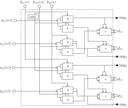
We define the interim registers tmp1=(a11◦b11), tmp2= (a12∗b21), tmp3=(a12◦b22), tmp5 =(a21◦b11), tmp6 = (a22∗b11), tmp7=(a22◦b22). These interim values are added to generated11,d12,d21,d22. Moreover, instead of having a general complex multiplication, we can employ the special functional components. For example, it is easy to verify that (a11◦b11)∗a∗11=pPow(tmp1,a11). By changing the compu-tation order and combining common compucompu-tations, we can finally show thatGis a Hermitian matrix with the elements given by
g11=pPow
tmp1,a∗11
+ 2tmp2,a∗11
+pPowtmp3,a∗12
,
g21=d21∗a11∗ +d22∗a12∗,
g12=g21∗,
g22=pPow
tmp5,a∗21
+ 2tmp6,a∗21
+pPowtmp7,a∗22
.
(30)
Thus the simplified M(A,B) RTL module can be de-signed as in Figure 6, with the input of both real and imaginary parts ofAas{a11(r/i),a12(r/i),a21(r/i),a22(r/i)}
and only the necessary elements of the Hermitian
b11(r) b21(r/i) b22(r)
a11(r/i)
a12(r/i)
a21(r/i)
a22(r/i)
conj o
∗
o ∗
o ∗
o ∗
+
+
+
+
tmp1
d11
d12
tmp3 tmp5
d21
d22
tmp7
Figure6: The simplified parallel VLSI RTL layout of theM(A,B) processing unit.
Pow (a, b) Pow (a, b) Re (a, b) A11
A21
A22
M(A21,A11)
T(A11,A21,A22)
(d21, d22) (a31, a32)
tmp(1,3,5,7)
g11
g22 ∗
∗ +
g21
T11
T21
T22
Figure7: The VLSI RTL architecture layout of theT(A11,A21,A22) block.
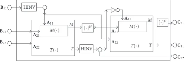
transformT(A11,A21,A22) of the (4×4) Hermitian matrix is given byFigure 7. The output ports of theT(A11,A21,A22) include the independent elements{t11,t21,t22}.
We can further simplify the top-level RTL schematic by extracting the commonality of theMandTmodule designs as inFigure 8to eliminate the extra individual M module. Thus, the results ofC11,C12, andC21are generated together
from the second T module. Compared with the design in
Figure 5, the architecture demonstrates better parallelism and reduced redundancy. The data path is much better bal-anced and facilitates the pipelining in multiple subcarriers for high-speed design.
If we use a standard computing architecture of the par-titioned (4×4) matrix inverse, we need 308 real multi-plications before dependency optimization (DO). With a
straightforward DO, the complexity is still 244 real multipli-cations. Traditionally, a complex multiplication is given by “c=cr+jci=(ar+jai)∗(br+jbi)=(arbr−aibi) +j(arbi+
aibr).” This has 4 real multiplications (RM) and 2 real
ad-ditions (RA). By rearranging the computation order, we can reduce the number of real multiplications as (1)p1 =arbr,
p2 = aibi, s1 = ar +ai, s2 = br +bi; (2) cr = p1− p2,
d = (p1+ p2), s = s1s2; (3) ci = s−d. This requires 3
HINV B11
B21
B22
A11
A21
A22
M(·)
T(·)
M
T
[·]H
HINV
A11
A21
A22
M(·)
T(·)
M
T
[·]H C21
C11
C22
Figure8: The commonality extracted VLSI design architecture based onT,M, and HINV.
5. COMPARATIVE PERFORMANCE AND
COMPLEXITY ANALYSIS
5.1. BER performance
The performance is evaluated in a MIMO-HSDPA simula-tion chain for different antenna configurations. We compare the performance of four different schemes: the LMS adap-tive algorithm, the CG algorithm, the FFT-based algorithm, and the DMI using Cholesky decomposition. We simulated the Pedestrian-A and Pedestrian-B channels following the I-METRA channel model [23], which are typical for high-speed downlink application. The chip rate for the transmit signal is 3.84 Mcps, which is in compliance with the 3GPP standard. The channel state information is estimated from the CPICH at the receiver. Ten percent of the total transmit power is dedicated to the pilot training symbols.
We provide the simulation results for QPSK modula-tion with antenna configuramodula-tion in the form of (M×N). In the figures, Lh is the channel delay spread. Figures 9
and10 show the fully loaded system for Pedestrian-A and Pedestrian-B channels with (2 × 2) configuration, while
Figure 11 shows a highly loaded system with 10 codes for (2×2) Pedestrian-B channel.Figure 12shows the simulation results for Pedestrian-A with (4×4) configuration. It can be seen that forFigure 9, the FFT-based algorithm overlaps with both the DMI and the CG at 5 iterations very closely. In a (2×2) case for Pedestrian-B channel, both the CG and FFT-based algorithms show very small divergence from the DMI at the very high SNR range inFigure 10. For a fully loaded system, CG with 5 iterations seems to be slightly better than FFT-based algorithm. But in a case with 10 codes, FFT-based algorithm outperforms the CG for both 3 iterations and 5 iterations. In the (4 ×4) case as shown in Figure 12, the FFT-based algorithm also outperforms the CG with 5 iter-ations. However, because the realistic system is most unlikely to work in the very high SNR range, the small difference in the BER performance is negligible. In all cases, the DMI, CG, and FFT-based algorithms significantly outperform the LMS adaptive algorithm.
It should be pointed out that the performance of the LMMSE-based chip equalizer is limited for the fast fading channel because of its block-based feature could not track the fast fading channel environments very well. To deal with this,
Table2: Complexity reduction for submatrix inverse inF−1.
Architecture RM
Traditional w/o DO(4×4) 308LF Traditional w/ DO(4×4) 244LF Hermitian opt(4×4) 90LF
a Kalman filter-based equalizer has been proposed in one of the authors’ papers [24] with much higher complexity. The discussion of the related architecture is out of the scope of this paper.
5.2. Complexity
The complexity is a very important consideration for real-time implementation. Although the complete equalizer sys-tem consists of the correlation/channel estimation, the tap solver, and the FIR filtering, we focus on the three-tap-solver complexity with similar performance, that is, the DMI, the CG, and the FFT-based algorithm. The other two parts are common for the algorithms presented here. Cholesky de-composition is assumed for the DMI. The complexity is com-pared in terms of number of equivalent complex multiplica-tions and addimultiplica-tions.
For the DMI, the complexity is at the order ofO((N(F+ 1))3) for the inverse ofR
rrandO((N(F+ 1))2M) for the
ma-trix multiplication in (Rrr)−1hm. For the conjugate gradient
algorithm, there areO{MJ[N(F+ 1)]2+M(5J+ 1)N(F+ 1)} complex multiplications andO{MJ[N(F+ 1)]2+ 8MJN(F+ 1)}complex additions. Usually,J =5 iterations for the CG algorithm will suffice for convergence near the DMI solution. For the FFT-based algorithm, the overall complexity before Hermitian optimization is O{(N2+ 2MN)L
F(log2LF)/2 +
(N3+MN2)L
F}. With the Hermitian optimization, the
com-plexity reduces toO{(N2/2 + 2MN)L
F(log2LF)/2 + (N3+
MN2)L
F/2}. For the FFT-based algorithm, we usually require
LF ≥2F+ 1. The complexity is summarized inTable 3. For
simplicity, we only list the most significant part of equivalent number of complex multiplications. An example is given for the (4×4) case withF=10,J=5. The length of FFTLF=32
0 2 4 6 8 10 12 14 16 SNR (dB)
10−4 10−3 10−2 10−1 100
Bi
t
er
ror
ra
te
LMS CG, 5 iter.
FFT-based DMI
Figure9: BER performance of 2×2 in Pedestrian-A channel;K=14,G=16,Lh=3,T=2,M=2, andF=10.
0 2 4 6 8 10 12 14 16 18 20
SNR (dB) 10−3
10−2 10−1 100
Bi
t
er
ror
ra
te
LMS FFT-based
CG, iter.=5 DMI
Figure10: BER performance of 2×2 in Pedestrian-B channel;K=14,G=16,Lh=6,T=2,M=2, andF=10.
In Figure 13, we show the complexity trend for differentJ
and differentLFversus the channel length for a (4×4)
sys-tem. Although the conjugate gradient algorithm has reduced complexity compared with the DMI, the complexity reduc-tion in the FFT-based algorithm is much more significant.
6. VLSI DESIGN ARCHITECTURE EXPLORATION
6.1. High-level-synthesis architecture scheduling
As a major revolution for the design of integrated circuits, SoC architecture leads to a demand in new methodologies and tools to address design, verification, and test problems in
0 2 4 6 8 10 12 14 16 SNR (dB)
10−3 10−2 10−1 100
Bi
t
er
ror
ra
te
LMS CG, iter.=3 CG, iter.=5
FFT-based DMI
Figure11: BER performance of 2×2 in Pedestrian-B channel case 2:K=10 codes;K=10,G=16,Lh=6,T=2,M=2, andF=10.
0 2 4 6 8 10 12 14 16
SNR (dB) 10−2
10−1 100
Bi
t
er
ror
ra
te
LMS CG, iter.=5
FFT-based DMI
Figure12: BER performance of 4×4 in Pedestrian-A channel;K=12,G=16,Lh=3,T=4,M=4, andF=10.
is presented in [13].
However, this type of SoC design space exploration is very time consuming because the current standard trial-and-optimize approaches apply hand-coded VHDL/Verilog or graphical schematic tools. In this section, we present a Catapult C-based HLS methodology [26] to explore the VLSI architecture space extensively in terms of the area/time tradeoff. This is enabled with high-level architecture and re-source constraints. Synthesizable RTL is generated from a fixed-point C/C++ level design and imported to the
Table3: The overall tap-solver complexity comparison.
Equivalent complex multiplication Example
DMI O(M+NF)(NF)2 92928
CG OJM(NF)2+ 5NF 43120
FFT-based ON2/2 + 2MNlog 2LF+
N3+MN2L F/2
5248
1 2 3 4 5 6 7 8 9 10
Number of filter tapsF
102 103 104 105
N
u
mber
of
co
mple
x
m
ult
DMI CG:J=5 CG:J=4
CG:J=3 FFT-based
LF=8
LF=16
LF=32
Figure13: Overall tap-solver complexity comparison; algorithm complexity comparison forM=4,N=4 tap solver.
Architecture constraint Algorithm
Architecture Ideas
Equations Floating-point
Fixed-point
Matlab C/C ++
Resource constraint Catapult C HLS scheduler
Hand-code schematic
IP cores HDL/ Verilog
Behavior model RTL model
Cycle accurate simulation
Mentor graphics advantage modelSim
Synthesis Place & route FPGA validation
Xilinx ISE Nallatech gate/netlist
Figure14: Integrated Catapult C high-level-synthesis design methodology.
which are either another Catapult C design or a legacy IP core. Leonardo spectrum is invoked for gate-level synthesis. Xilinx ISE place & route tool is used to generate gate-level bit-stream file. Raising the language level may lead to
Output DPRAM P
R S P/S A
C R . . . . . . I M
R .
. . . . . P M S
Input-shift-latches
Chip update r[i]
STARTRD Nchip RDY FSM/
MUX controller Parameters
Chip clk
FUBM FUBA
Figure15: Throughput mode correlation update module using PMS.
design flow. In most cases, the manual tradeoffstudy of a complex design with hundreds of multipliers could be ex-tremely time consuming and difficult. However, we can al-most achieve the al-most efficient design architecture for a given specification using the architecture scheduling in Catapult C, especially for the computation-intensive algorithms. Com-pared with the conventional hand-code and schematic-based design methodologies, the Catapult C-based methodology demonstrates not only improved productivity, but also a ca-pability to study the architecture tradeoffs extensively in a short design cycle.
6.2. Real-time VLSI architecture exploration
The complete equalizer includes two major steps: the com-putation of the equalizer coefficientsw and the actual FIR filtering using the updated equalizer taps as inwHr
A(i). The
update of the equalizer coefficients is a block-based opera-tion depending on the channel varying speed. The FIR filter-ing depends on the chip rate. Thus, we need to compute the
L-tap convolution for each input chip from theNreceive an-tennas for the FIR filtering within fclk/ fchipcycles, where fclk andfchipare the system clock rate and chip rate, respectively. The WCDMA chip rate is 3.84 MHz. We applied a clock rate of 38.4 MHz for theXilinxVirtex-II V6000-4 FPGA. There will be 10 cycles time constraint per input chip. For the tap solver, the experiment shows that 2 updates per slot are suf-ficient to provide acceptable performance for slow and me-dian fading channels. Since there are 1920 chips per slot, the latency requirement for each update is 250 microseconds.
We schedule architectures in two basic modes according to the real-time behavior of the subsystem in Catapult C: the throughput mode or the block mode. Throughput mode
as-sumes that there is a top-level main loop for each incoming sample, which is processed immediately in the computation period. The module processes for each input sample period-ically, so there is a strict limit for the processing time. Block-mode processes once after a block data is ready. Because the finite-state machine (FSM) usually depends on complex logic and extensive memory access, the computation patten is more like a processor architecture in loading data to the functional units. In the following, we use two typical design modules to demonstrate these different working modes.
6.2.1. Scalable pipelined-multiplexing scheduler
The covariance estimation is computed as
Rrr =
1
NB
NB−1
i=0
rA(i)rHA(i) (31)
assuming ergodicity. Theoretically, the front-end covariance estimation module can also be designed in block mode sim-ilar to a processor implementation. However, this architec-ture causes a large processing latency and requires big ping pong buffers to store the input samples. ForNB =960 chips
Table4: Architecture tradeoffexploration for covariance estima-tion module.
Cycles 1 2 3 4–8 9 10
MU(a) 0 176 0 0 0 0
AD(a) 0 0 136 0 0 0
MU(b) 0 22 22 22 22 0 AD(b) 0 0 17 17 17 17
(ACR). After the word length is adjusted by shifting, a separate parallel-read-shuffle (PRS) module designed by Catapult C reads the registers in parallel for [E0,. . .,EL] and
writes the memory and shuffles the Hermitian part [EH L,
. . .,EH
1]. Memory stalls are avoided and scalability is achieved because it can stop at any chip to adjust to different update rates.
In the PMS, the number of FUs is assigned according to the time/area constraints. As an example for a (2×2) case with L = 10, the VLSI area/time tradeoffis shown in
Table 4. The complexity is 176 multiplications and 136 ad-ditions in each computation period. A typical manual de-sign will layout 176 multipliers and 136 adders all in parallel. This will take 4 cycles to complete the computation. How-ever, the multipliers are in IDLE state for 9 cycles and wasted. On the other extreme, an area-constraint solution will reuse one multiplier and one adder, but has to take more than 176 cycles. The most area/time efficient architecture in 10 cy-cles is to reuse 22 multipliers and 15 adders as the pipelined operations. The multiplexing of so many multipliers in man-ual RTL layout could be very difficult and time consuming. Moreover, for a changed specification such as the chip rate or clock rate, we can rapidly reschedule the design to meet the real-time requirement by using the minimum hardware re-source. The similar design method is applied for the FIR and channel estimation.
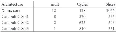
6.2.2. Block-based MIMO-FFT IP cores
For the multiple FFTs in the tap solver, the keys for optimiza-tion of the area/speed are loop unrolling, pipelining, and re-source multiplexing. Although Xilinx provides FFT IP cores, they are considerably large and much faster than required. For example, a single v32FFT core in Xilinx CoreGen library utilizes 12 multipliers and 2066 slices. Moreover, it is not easy to apply the commonality by using the IP core for the MIMO-FFTs. To achieve the best area/time tradeoffin diff er-ent situations, we design the customized MIMO-FFT mod-ules to utilize the commonality in control logic and phase co-efficient loading. Parallelism/pipelining in the parallel FFTs are studied extensively in multilevels, for example, the BFU level, the stage level, and the FFT-processor level. Catapult C scheduled RTLs for 32-point FFTs with 16 bits are com-pared with Xilinx v32FFT Core inTable 5for a single FFT. Catapult C design demonstrates much smaller size for diff er-ent solutions, for example, from solution 1 with 8 multipli-ers and 535 slices to solution 3 with only one multiplier and 551 slices. Overall, solution 3 represents the smallest design
Table5: Architecture efficiency comparison for Catapult C versus Xilinx IP core.
Architecture mult Cycles Slices Xilinx core 12 128 2066 Catapult C Sol1 8 570 535 Catapult C Sol2 2 625 543 Catapult C Sol3 1 810 551
Table 6: The area/time specification of the major FPGA design cores.
Architecture Latency CLB ASICMult Correlator 1 chip 22399 80 16-FFT32 43.1μs 2530 4 32 MatInvMult(4×4) 37.6μs 4526 6 16-IFFT32 43.1μs 2530 4 Overall tap solver 123.8μs 7109.3 14
with slower but acceptable speed for a single FFT. For the MIMO-FFT/IFFT modules, we can reuse the control logic in-side the FFT module and schedule the number of FUs more efficiently in the merged mode.
6.3. Prototyping implementation
Based on the above algorithmic and architectural optimiza-tions, we have prototyped the VLSI architecture of a (4×4) MIMO equalizer on theAptixFPGA platform [27]. The cor-relation window is set to 10 chips for all 4 receive anten-nas. Fixed-point simulation shows that 8-bit input chip could provide negligible performance loss. To give a safe range, the input chip samples to both the corelator and the channel esti-mator have 10-bit precision. The 32-point MIMO-FFT mod-ule has 16-bit input word length for both the covariance and channel coefficients. To support even faster fading speed, we design the prototyping system for up to 4 updates per slot with an overall tap-solving latency requirement of 125 mi-croseconds. InTable 6, we give the specification of the ma-jor design blocks. Overall, we utilize only 4 multipliers to achieve area/time efficient design for 16 merged FFT/IFFT modules. For the LFinverse of the (4×4) Hermitian