IJEDR1404042
International Journal of Engineering Development and Research (www.ijedr.org)3656
Design and Implementation of Parallel AES
Encryption Engines for Multi-Core Processor Arrays
M.Sambasiva Reddy
1, P.James Vijay
2, B.Murali Krishna
3 Assistant Professor1, Assistant Professor2, Assistant Professor3 Dept. Of Electronics and Communication Engineering Sree Vahini Institute of science&Technology, Tiruvuru,India________________________________________________________________________________________________________
Abstract - By exploring different granularities of data-level and task-level parallelism, we map 4 implementations of an Advanced Encryption Standard (AES) cipher with both online and offline key expansion on a fine-grained many-core system. The smallest design utilizes only six cores for offline key expansion and eight cores for online key expansion, while the largest requires 107 and 137 cores, respectively. In comparison with published AES cipher implementations on general purpose processors, our design has 3.5-15.6 times higher throughput per unit of chip area and 8.2-18.1 times higher energy efficiency. Most AES calculations are done in a special field. The AES cipher is specified as a number of repetitions of transformation rounds that convert the input plain-text into the final output of cipher-text. Each round consists of several processing steps, including one that depends on the encryption key. A set of reverse rounds are applied to transform cipher-text back into the original plain-text using the same encryption key.
Key words- -Advanced Encryption Standard, Sub bytes, Shift row, mixed column, Add round Key and Parallel AES.
________________________________________________________________________________________________________
I. INTRODUCTION
Cryptography is the practice and study of hiding information. Applications of cryptography include ATM cards, computer passwords, until modern times cryptography referred almost exclusively to encryption, which is the process of converting ordinary information into unintelligible gibberish. Decryption is the reverse, in other words, moving from the unintelligible cipher text back to plaintext. A cipher is a pair of algorithm which creates the encryption and the reversing decryption. The detailed operation of a cipher is controlled both by the algorithm and in each instance by a key. With the development of information technology, protecting sensitive information via encryption is becoming more and more important to daily life. In 2001, the National Institute of Standards and Technology selected the Rijndael algorithm as the Advanced Encryption Standard (AES), which replaced the Data Encryption Standard (DES). Since AES has been widely used in a variety of applications, such as secure communication systems, high-performance database servers, digital video/ audio recorders, and smart cards.
The Advanced Encryption Standard (AES) is an encryption standard that comprises three block ciphers, AES-128, AES-192 and AES-256, adopted for different applications. AES is one of the most popular algorithms used in symmetric key cryptography. It is available in many different encryption packages. AES is based on a design principle known as a Substitution permutation network. It is fast in both software and hardware, is relatively easy to implement, and requires little memory. AES has a fixed block size of 128 bits and a key size of 128, 192, or 256 bits, whereas Rijndael can be specified with block and key sizes in any multiple of 32 bits, with a minimum of 128 bits and a maximum of 256 bits. Assuming one byte equals 8 bits, the fixed block size of 128 bits is 16 bytes. AES operates on a 4×4 array of bytes, termed the state.
A set of reverse rounds are applied to transform cipher-text back into the original plain-text using the same encryption key. The proposed architecture is FPGA based architectures with high-speed and low area constraints for suitable implementation of Advanced Encryption Standard (AES). The main focus of this paper is to compare different design architectures existing in literature with the proposed ones, based on application specific constraints. Most AES calculations are done in a special field. The AES cipher is specified as a number of repetitions of transformation rounds that convert the input plain-text into the final output of cipher text. Each round consists of several processing steps, including one that depends on the encryption key.
II.RELATED WORK
IJEDR1404042
International Journal of Engineering Development and Research (www.ijedr.org)3657
trade-off for an ASIC implementation of the Advanced Encryption Standard(AES).Different pipelined implementations of the AES algorithm as well as the design decisions and the area optimizations that lead to a low area and high throughput AES encryption processor are presented. With loop unrolling and outer-round pipelining techniques, throughputs of 30 Gigabits/s to 70 Gigabits/s are achievable in a 0.18-_m CMOS technology. Moreover, by pipelining the composite field implementation of the byte substitution phase of the AES algorithm (inner-round pipelining), the area consumption is reduced up to 35 percent. By designing an offline key scheduling unit for the AES processor the area cost is further reduced by 28 percent, which results in a total reduction of 48 percent while the same throughput is maintained. Therefore, the over 30 Gigabits/s, fully pipelined AES processor operating in the counter mode of operation can be used for the encryption of data on optical links.[4] Describes an on-die, reconfigurable AES encrypt/decrypt hardware accelerator fabricated in 45 nm CMOS, targeted for content-protection in high-performance microprocessors. 100% round computation in native composite-field arithmetic, unified reconfigurable data path for encrypt/decrypt, optimized ground & composite-field polynomials, integrated affine/bypass multiplexer circuits, fused Mix/InvMixColumn circuits and a folded Shift Row data path enable peak 2.2 Tbps/Watt AES-128 energy efficiency with a dense 2-round layout occupying 0.052 mm_, while achieving: (i) 53/44/38 Gbps AES-128/192/256 performance, 125 mW, measured at 1.1 V, 50 C, (ii) scalable AES-128 performance up to 66 Gbps, measured at 1.35 V, 50 C, (iii) wide operating supply voltage range with robust sub threshold voltage performance of 800 Mbps, 409 W, measured at 320 mV, 50 C (iv) 37% Sbox delay reduction and 25% area reduction with a compact Sbox layout occupying 759 m_ (v) 67% reduction in worst-case interconnect length and 33% reduction in Shift Row wiring tracks and (vi) 43% reduction in Mix/InvMixColumn area with no performance penalty. [5] Describes A 167-Processor Computational Platform in 65 nm CMOS A 167-processor computational platform consists of an array of simple programmable processors capable of per-processor dynamic supply voltage and clock frequency scaling, three algorithm-specific processors, and three 16 KB shared memories; and is implemented in 65 nm CMOS. All processors and shared memories are clocked by local fully independent, dynamically halt able, digitally-programmable oscillators and are interconnected by a configurable circuit-switched network which supports long-distance communication. Programmable processors occupy 0.17 mm and operate at a maximum clock frequency of 1.2 GHz at 1.3 V. At 1.2 V, they operate at 1.07 GHz and consume 47.5 mW when 100% active, resulting in an energy dissipation of 44 pJ per operation. At 0.675 V, they operate at 66 MHz and consume 608 W when 100% active, resulting in a total energy dissipatio n of 9.2 pJ per ALU or MAC operation.
[6] Presents a globally-asynchronous locally synchronous (GALS)-compatible circuit-switched on-chip network that is well suited for use in many-core platforms targeting streaming digital signal processing and embedded applications which typically have a high degree of task-level parallelism among computational kernels. Inter-processor communication is achieved through a simple yet effective reconfigurable source synchronous network. Interconnect
Paths between processors can sustain a peak throughput of one word per cycle. A theoretical model is developed for analyzing the performance of the network. A 65 nm complementary metal–oxide–semiconductor GALS chip utilizing this network was fabricated which contains 164 programmable processors, three accelerators and three shared memory modules. For evaluating the efficiency of this platform, a complete 802.11a wireless local area network baseband receiver was implemented. It has a real-time throughput of 54 Mb/s with all processors running at 594 MHz and 0.95-V, and consumes an average of 174.8 mW with 12.2 mW (or 7.0%) dissipated by its interconnect links and switches. With the chip’s dual supply voltages set at 0.95-V and 0.75-V, and individual processors’ oscillators operating at workload-based optimal frequencies, the receiver consumes 123.2 mW, which is a 29.5% reduction in power. Measured power consumption values from the chip are within 2–5% of the estimated values. [7] Presents the many-core architecture, with hundreds to thousands of small cores, to deliver unprecedented compute performance in an affordable power envelope. We discuss fine grain power management, memory bandwidth, on die networks, and system resiliency for the many-core system. Conversion to 450mm diameter can only occur if the economic advantages can be demonstrated for the entire supply chain. In previous diameter conversions, chip makers have not been overly concerned about the effect of the conversion on silicon wafer manufacturers. The change to 450 mm wafers, however, may be significantly different because of the magnitude of the financial burden placed upon the wafer producers. The extent of this burden will be estimated later in this paper, and some of its consequences will be explored.
III.EXISTING SYSTEM
IJEDR1404042
International Journal of Engineering Development and Research (www.ijedr.org)3658
IV. PROPOSED SYSTEM
A. Parallel Advanced Encryption Standard (AES)
The proposed system Parallel AES is a symmetric encryption algorithm, and it takes a 128-bit data block as input and performs several rounds of transformations to generate output cipher text. Each 128-bit data block is processed in a 4-by-4 array of bytes, called the state. The round key size can be 128, 192 or 256 bits. The number of rounds repeated in the AES, Nr, is defined by the length of the round key, which is 10, 12 or 14 for key lengths of 128, 192 or 256 bits,
B. steps involved
First Step: Sub Bytes, a non-linear substitution step where each byte is replaced with another according to a lookup table.
Second Step: Shift Rows, a transposition step where each row of the state is shifted cyclically a certain number of steps.
Third Step: Mix Columns, a mixing operation which operates on the columns of the state, combining the four bytes in each column.
Fourth Step: Add Round Key, each byte of the state is combined with the round key; each round key is derived from the cipher key using a key schedule.
V.EXPERIMENTAL RESULTS
Model Sim Se6.3f Simulator provides unified mixed language simulation engine for the fastest regression suite throughput native support of verilog, system verilog for design, vhdl, and systemC for effective verification Model Sim’s advanced code coverage capabilities and ease of use lower the barriers for leveraging this valuable verification resource. ModelSim combines simulation performance and capacity with the code coverage and debugging capabilities required to simulate multiple blocks and systems and attain ASIC gate-level sign-off. Comprehensive support of Verilog, System Verilog for Design, VHDL, and SystemC provide a solid foundation for single and multi-language design verification environments.
IJEDR1404042
International Journal of Engineering Development and Research (www.ijedr.org)3659
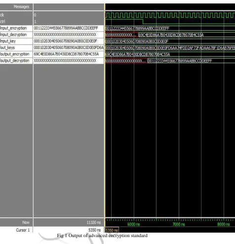
Fig 1 Output of advanced encryption standardThe above figure represents output of a single aes engine. It will show the encryption and decryption process simultaneously. Data and keys are represented in the form of hexadecimal values for quick reference.
IJEDR1404042
International Journal of Engineering Development and Research (www.ijedr.org)3660
Fig 2: Output e of parallel aes engineThe Fig 2 illustrates the output of four aes engines performs as parallel. Encryption done at enable pin value 1 and decryption for enable pin 0. Data represented in hexadecimal form and parallel four encryption and decryption shown in figure.
VI.CONCLUSION
We have presented 4different AES cipher implementations with both on offline key expansion on a fine-grained many-core system. Each implementation exploits different levels of data and task parallelism. The smallest design requires only six processors, equalling 1:02 mm2 in a 65 nm fine-grained many-core system. The fastest design achieves a throughput of 4.375 cycles per byte, which is 2.21 Gbps when the processors are running at a frequency of 1.2 GHz. We also optimize the area of each implementation by examining the workload of each processor, which reduces the number of cores used as much as 18 percent. The design on the fine-grained many core system achieves energy efficiencies approximately 2.9-18.1 times higher than other software platforms, and performance per area on the order of 3.3-15.6 times higher. Overall, the fine-grained many-core system has been demonstrated to be a very promising platform for software AES implementations.
REFERENCES
IJEDR1404042
International Journal of Engineering Development and Research (www.ijedr.org)3661
[2] S. Morioka and A. Satoh, “A 10-gbps full-AES Crypto Design with a Twisted BDD s-Box Architecture,” IEEE Trans. VeryLarge Scale Integration Systems, vol. 12, no. 7, pp. 686-691, July 2004.
[3] A. Hodjat and I. Verbauwhede, “Area-Throughput Trade-Offs for Fully Pipelined 30 to 70 Gbits/s AES Processors,” IEEE Trans. Computers, vol. 55, no. 4, pp. 366-372, Apr. 2006.
[4] S.K. Mathew, F. Sheikh, M. Kounavis, S. Gueron, A. and R.K. Krishnamurthy, “53 gbps Composite-Field AES-Encrypt/Decrypt Accelerator for Content-Protection in 45 nm High-Performance Microprocessors,” IEEE J. Solid-State Circuits, vol. 46, no. 4, pp. 767-776, Apr. 2011.
[5] D.N. Truong, W.H. Cheng, T. Mohsenin, Z. Yu, A.T. Jacobson, G. Landge, M.J. Meeuwsen, A.T. Tran, Z. Xiao, E.W. Work, J.W. Webb, P. Mejia, and B.M. Baas, “A 167-Processor Computational Platform in 65 nm CMOS,” IEEE J. Solid-State Circuits, vol. 44, no. 4, pp. 1130-1144, Apr. 2009.
[6] S. Borkar, “Thousand Core Chips: A Technology Perspective,” Proc. 44th Ann. Design Automation Conf., pp. 746-749, 2007.
[7] A.T. Tran, D.N. Truong, and B.M. Baas, “A Reconfigurable Source-Synchronous On-Chip Network for GALS Many-Core Platforms,” IEEE Trans. Computer-Aided Design of Integrated Circuits and Systems, vol. 29, no. 6, pp. 897-910, June 2010. [8] X. Zhang and K. K. Parhi, “On the optimum constructions of composite field for the AES algorithm,” IEEE Trans. Circuits
Syst. II, Exp. Briefs, vol. 53, no. 10, pp. 1153–1157, Oct. 2006.
[9] S X. Zhang and K. K. Parhi, “High-speed VLSI architectures for the AES algorithm,” IEEE Trans. Very Large Scale Integer. (VLSI) Syst., vol. 12, no. 9, pp. 957–967, Sep. 2004.
[10] and A. Satoh, “A 10-gbps full-AES Crypto Design with a Twisted BDD s-Box Architecture,” IEEE Trans. Very Large Scale Integration Systems, vol. 12, no. 7, pp. 686-691, July 2004.
[11] A. Hodjat and I. Verbauwhede, “A 21.54 gbits/s Fully Pipelined AES Processor on FPGA,” Proc. IEEE 12th Ann. Symp. Field-Programmable Custom Computing Machines, pp. 308-309, Apr. 2004.
[12] J. Chang, C.-W. Huang, K.-H. Chang, Y.-C. Chen, and C.-C.Hsieh, “High Throughput 32-Bit AES Implementation in FPGA, ”Proc. IEEE Asia Pacific Conf. Circuits and Systems, pp. 1806-1809, Nov. 2008.
[13] J. Granado Criado, M. Vega-Rodriguez, J. Sanchez-Perez, and J.Gomez-Pulido, “A New Methodology to Implement the AES Algorithm Using Partial and Dynamic Reconfiguration,” Integration, the VLSI J., vol. 43, no. 1, pp. 72-80, 2010. [14] S. Qu, G. Shou, Y. Hu, Z. Guo, and Z. Qian, “High Throughput, Pipelined Implementation of AES on FPGA,” Proc.Int’l