IJEDR1602096
International Journal of Engineering Development and Research (www.ijedr.org)538
Modeling, Simulations and DSP Implementation of
H-Bridge SMLI with Different Modulation
Techniques
1D.P.Maheshwari, 2Prof. Dr. A.S.Pandya,
1Research scholar at Kadi University, 2Principal of AVPT, Rajkot, 1Vishwakarma Government Engineering College, Chandkheda, Ahmedabad.
_______________________________________________________________________________________________________
Abstract - Paper presents comparative study and simulation results for Hybrid Multilevel Inverter configuration employing different modulation techniques..The operating principle of each topology is discussed with a review of the relevant modulation method focusing mainly on total harmonic distortion (THD). Such multilevel inverters achieve higher power quality with a given switch count when compared to traditional multilevel inverters. The purpose of the circuits presented here is to minimize the reverse voltage stress that affects the power switches and decrease the harmonic distortion of the voltage applied to the load
Index Terms - Hybrid MLI, Frequency, Voltage Output.
_______________________________________________________________________________________________________ Paper includes the theory of the Hybrid and Symmetrical Hybrid type multilevel inverter (MLI) and their advantages. The classification of MLIs according to the source are also given in this chapter. The various control techniques to control the symmetrical type multi level inverter are SPWM, POD, PD. Implementation using DSP is also discussed.
I.INTRODUCTION
Two classes of multilevel inverter according to the voltage source: Symmetrical type Multi Level Inverter and Asymmetrical type Multi Level Inverter [1], [2] .In symmetrical multilevel inverter all H-bridge cells are fed by equal voltages and hence all the arm cells produce similar output voltage steps [3]. If all the cells are not fed by equal voltages, the inverter becomes an asymmetrical one and cells have different effect on the output voltage. [4-6]
The multilevel inverters based on the H-bridge symmetrical cascade have a number of levels in its output voltage given by 2N+1. Its output voltage levels are also obtained through the same expression. Therefore, we have 2N+1 levels in the load, where N is the number of DC sources. Fig 1 represents a five-level output voltage single-phase inverter. The Three level Cell (TC) switches block voltages of value ´E´, and with proper modulation strategy they operate at high frequency (a few kHz). On the other hand, the H-bridge switches (S5, S6, S7 and S8) must block a higher voltage level of ‘2E’. These switches operate at low frequency commutating at zero voltage. Hence it falls into the hybrid multilevelinverters group.With a proper driving pattern for switches S1 - S4, and for the switches S5-S6 of the H-Bridge, it is possible to obtain desired voltage waveform between the points A-B.[7]
Fig 1 Single-phase Symmetrical Hybrid multilevel Inverter(SHMLI) based on three-level cell
IJEDR1602096
International Journal of Engineering Development and Research (www.ijedr.org)539
II.MODULATION TECHNIQUES FOR HMLI
The inverter output can be changed and controlled according to the desired level by the triggering pulse given to the gate terminal in the inverter. This controlling method is obtained by various modulation technique. The pulse is used as a triggering pulse for the gate terminal of the power devices which is used to ON and OFF the power devices. Pulse width modulation techniques for controlling the multilevel inverter topologies are step modulation, sinusoidal PWM, space vector modulation, selective harmonic PWM, modified sinusoidal PWM and multiple pulses PWM.
PWM strategies with differing phase relationships: [4]
1. Alternate phase disposition (APOD) - every carrier waveform is in out of phase with its neighbouring carrier by 180°.
2. Phase opposition disposition (POD) - All carrier waveforms above zero reference are in phase and are 180° degree are out of phase with those below zero.
3. Phase disposition (PD) - All carrier waveforms in phase.
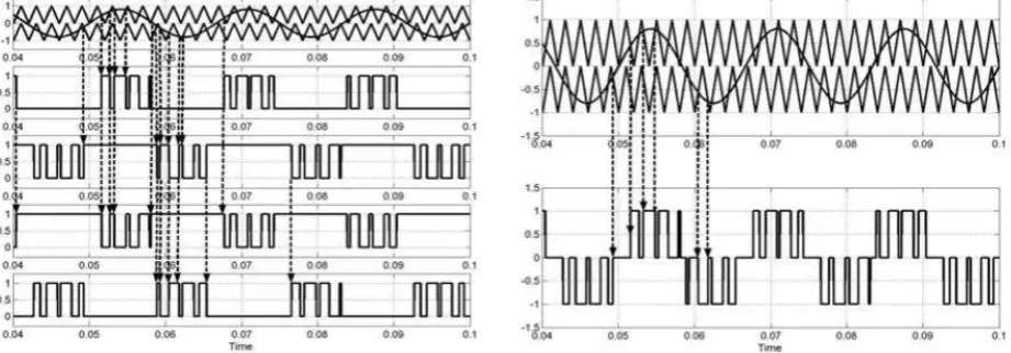
Alternate Phase Disposition (APOD)
Every carrier waveform is in out of phase with its neighbor carrier by 180° degree.
Fig 3 Switching Pattern and Output Waveform using the APOD carrier-based PWM scheme
.
Phase Opposition Disposition (POD)
For phase opposition disposition (POD) modulation all carrier waveforms above zero reference are in phase and are 180° out of phase with those below zero.
Phase Disposition (PD)
Paper discusses the carrier-based implementation the phase disposition PWM scheme.Fig.4 depicts the sine-triangle method for a three-level inverter. Therein, the a-phase modulation signal is compared with two (n-1 in general) triangle waveforms.
Fig 5 Pattern Switching and Simulation Output Waveform using the PD Scheme III.SHMLISIMLUATIONMODELS
IJEDR1602096
International Journal of Engineering Development and Research (www.ijedr.org)540
SPWM
Fig 6: SIMULATION Model: SHMLI USING SPWM with R LOAD
Switching Pulses for ( s1 & s2) and (s3 & s4)
IJEDR1602096
International Journal of Engineering Development and Research (www.ijedr.org)541
Phase Opposition Disposition (POD)
Fig 8: SIMULINK Model : POD
Control Signals : POD OUTPUT Fig 9 : Simulation Results : POD
Phase Disposition PD
IJEDR1602096
International Journal of Engineering Development and Research (www.ijedr.org)542
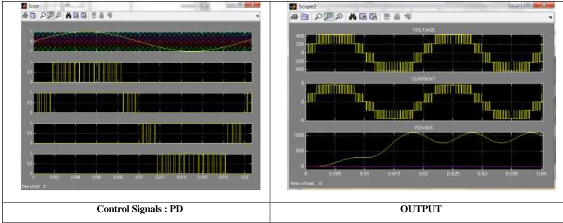
Control Signals : PD OUTPUT Fig 11 : Simulation Results : PD
IV.DSPBASED IMPLEMENTATION
11 HMLI Power Circuit Setup with DSP Kit ( 2812 )
Fig 12 Block Diagram of the Hardware Setup with DSP Kit
MATLAB/SIMULINK & CCS Interface with DSP Kit
The interfacing of code composer studio and MATLAB/SIMULINK and DSP 320F2812 kit through Emulator after generating code in CCS by clicking on build option on MATLAB.[11]
All the Components are discrete fix step use with sampling frequency of 2x10⁻⁵. Discrete Triangular carrier wave is generated is generated by differentiating discrete square wave.
Discretization of Simulation models isdone before going to DSP code generation for simulink model depicted in previous section.[11]
BUFFER ,
OPTO-COUPLER
And
Driver
POWER CIRCUIT( SHMLI )
DC POWER SUPPLY
IJEDR1602096
International Journal of Engineering Development and Research (www.ijedr.org)543
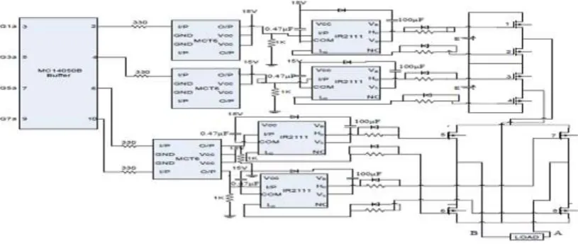
MOSFET Driver Module
Fig 13 MOFFET driver module used in the implemented prototype
Fig- 13 shows the MOSFET driver module used in the implemented prototype. It requires an single isolated voltage source and the driver signal. Isolation is provided on the module by opto-isolator. The gating signals from Buffer are given to bridge module. On the module this signals first isolated using opto-isolator MCT-6. The IR2111 is used as driver IC for MOSFET switches.Output of opto-isolator is configured as common collector mode and hence provide non-inverting signals. The IC IR2111 require only one input for upper (Higher) MOSFET of the leg. The gate pulse for lower MOSFET automatically generated by inverting Higher gate pulse in the driver IC to provides the dead-band of 650 nanosecond with provided protection against turn on and turn off time delay. The IRF840 (500V, 8A) N-channel MOSFET is used for switching purpose.[10]
Experimental Waveforms
DSP 2812 was used for the control signal generation for the MOSFETs of the single phase H bridges three level switches (TC). [12]
With CCS installed and configured, MATLAB returns a list of the boards that CCS recognizes on PC As follows: 1 F2812 Simulator 0 CPU TMS320C28xx
0 F2812 PP Emulator 0 CPU_1 TMS320C28xx
After setting up Matlab/CCS support to DSK kit, follow steps given below…
1. Remove Power Circuits from model and retain Control circuit for implementation. 2. Open Configuration Parameters from Simulation menu:- Select Fix Step Discrete and 3. set sampling rate, i.e. 2e-5, Apply and Ok.
4. Open Simulink library browser:- Select the processor, i.e. F2812 ezdsp from target 5. support packages.
6. Place and configure your input/output ports i.e. ADC, GPIO or PWM for the selected 7. processor.
8. Use 28x IO math/ DMC block components from library browser foroptimization. 9. Discrete all model blocks, such that there must not be any continuous state. 10. Change appropriate output data signal type or use data type conversion. 11. Run your model and save your model if no errors are indicated
12. Run ccs setup: Set target Connection parameter(simulator or emulator),i.e.F2812 Device simulator, or XDS 510 F2812 device emulator and save and exit.
13. From your simulink model click on build target or press Ctrl+B on key board. 14. Require code will automatically generated though CCS and will be loaded to kit 15. Using JTAG emulator.
IJEDR1602096
International Journal of Engineering Development and Research (www.ijedr.org)544
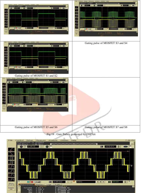
Gating pulse of MOSFET S1 and S2Gating pulse of MOSFET S3 and S4
Gating pulse of MOSFET S5 and S6 Gating pulse of MOSFET S7 and S8
Fig 14 : Gate Pulses generated by DSP kit
Fig 15: Output of SHMLI – Power Circuit
V.DISCUSSION OF RESULTS
IJEDR1602096
International Journal of Engineering Development and Research (www.ijedr.org)545
Sr. No. Modulation Technique THD
1 SPWM 1.23
2 POD 1.25
3 PD 1.24
Table-1 THD from Simulation Study
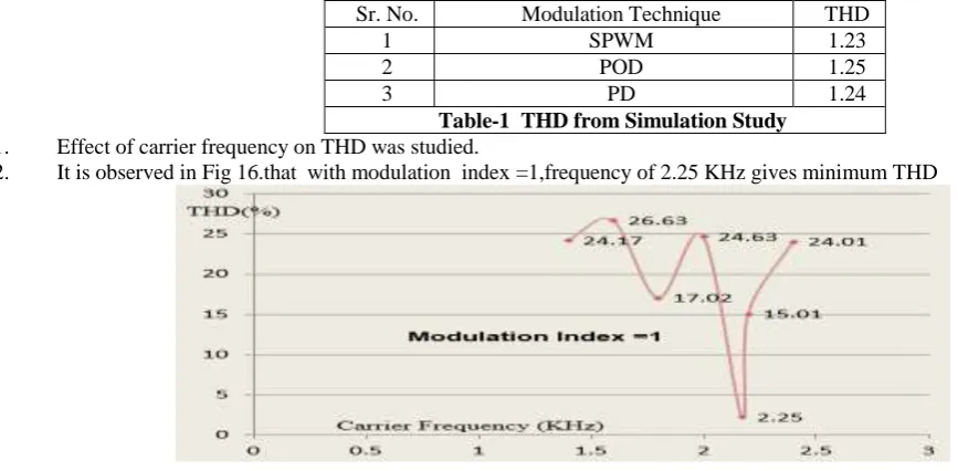
1. Effect of carrier frequency on THD was studied.
2. It is observed in Fig 16.that with modulation index =1,frequency of 2.25 KHz gives minimum THD
Fig 16 Analysis H MLI : CARRIER FREQUENCY(Fc) v/s THD(%)
3. Effect of modulation index on THD was investigated It is observed in Fig 18.that with frequency of 2.25 KHz as shown in the figure 17.
Fig 18 Analysis H MLI :Modulation Index v/s THD(%) @ 2.2 KHz
VI.REFERENCES
[1] Madhav D. Manjrekar and Thomas A. Lipo, “A hybrid multilevel inverter topoloyfor drive applications”. Applied Power Electronics Conf. and Exp., IEEE-APEC 1998.
[2] Madhav D. Manjrekar, Peter Steimer and Thomas A. Lipo, “Hybrid Multilevel Power Conversion System: a competitive solution for high power applications”. IEEE Transaction on Industry Applications, Vol. 36, No3, pp.834-841 May/june 2000.
[3] Leon M. Tolbert, Fang ZhengPeng and Thomas G. Habetler, “Multilevel Converters for Large Electric Drives”. IEEE Transactions on Industry Applications, vol. 35, N° 1, january/february 1999.
[4] Rashid M. H., 2004. Power Electronics: Circuits, Devices, and Applications, 3rd edition Englewood Cliffs, NJ:Prentice-Hall.
[5] Choi N. S, et al., “ A General Circuit Topology of Multilevel Inverter”, IEEE Power Electronics Specialists Conference,Vol. 22, pp. 96-103,1991.
[6] C. Govindaraju and K. Baskaran, “Performance analysis of cascaded multilevel inverter with hybrid phase-shifted carrier modulation, ” Aust. J. Electr. Electron. Eng., vol. 7, no. 2, pp. 121–132, Jun. 2010.
[7] J. Wen and K. M. Smedley, “Synthesis of multilevel converters based on single- and/or three-phase converter building blocks,” IEEE Trans. Power Electron., vol. 23, no. 3, pp. 1247–1256, May 2008.
[8] F. Peng and J. S. Lai, “Multilevel cascade voltage source inverter with separate DC sources,” U.S. Patent 5 642 275, Jun. 24, 1997.
[9] T. A. Lipo and M. D. Manjrekar, “Hybrid topology for multilevel power conversion,” Patent W.O. 99/41 828, Aug. 19, 1999.
[10]Mathworks Inc., USA “User Manual MATLAB”
[11]Texas Instruments : Getting Started with Code Composer Studio
IJEDR1602096
International Journal of Engineering Development and Research (www.ijedr.org)546
BIO-GRAPHY
Prof.D.P.Maheshwari is associate professor in electrical engineering department at Vishwkarma Government Engineering College, Chandkheda. He received his BE and ME degree from Saurastra University and Rajiv Gandhi Proudyogiki Vishwavidyalaya, Bhopal respectively. He has over 15 years of teaching experience. His areas of interest are Power Electronics and Drives.