Dynamic Shift Scan with Area Efficiency
Ancy Joy1, Sani John2
Assistant Professor, Dept. of ECE, SCET, Trissur, Kerala, India1
Assistant Professor, Dept. of ECE, VJCET, Ernakulam, Kerala, India2
ABSTRACT: Sequential circuit testing is more effective if it is done using dynamic shift scan method. Again the testing of sequential circuits can be done in minimum clock cycles by using a cycle cycle access with hold mode. Here the advantage is it reduces the clock cycles and the problem is it increases the hardware. The percentage of utilization again can be reduce by the modification of scan cells. Each scan cells can be change to single cycle access without hold mode. It reduces the clock cycles and reduces the area utilization also.
KEYWORDS:Sequential Circuits, Single Cycle Access, Scan Cells, Testing Time
I.INTRODUCTION
Testing these cores requires a large amount of test data, which is continuously increasing with the rapid increase in the complexity of SOC. This has a direct impact on the total testing time and the memory requirements of the testing equipment. Hence, reducing the amount of test data is considered as one of the challenging problems in testing. More techniques for test power minimization are surveyed from the literatures. Test data transformations are also carried out to reduce the transitions during shift cycle and hence test power. The methods surveyed are having more logics to reduce power but with the cost of other parameters like test area overhead and testing speed. In this project, a novel method is proposed to reduce the hardware area by modifying the design of scan architecture.
As the number of cores integrated in a System-on-a-Chip (SoC) increases, the number of top-level pins is often less than that required to test the cores in parallel. To reduce the test application time, the efficiency of utilizing limited tester bandwidth must be improved. The tester bandwidth can be reduced through dynamic allocation of the channel inputs feeding different cores in the SoC. Another way to improve the tester bandwidth without dynamically allocating the channel inputs is to reduce the number of channels used by each core. Testing each core with an extremely high compression configuration allows more cores to be tested in parallel. Unfortunately, reducing the number of channel inputs feeding to a core implies lower encoding capacity. As a result, testable faults may become undetected due to lack of encoding capacity. More test patterns are also often needed to achieve the same test coverage since fewer faults can be detected by each test cube during dynamic compaction. Here the scan cells are modified as single cycle access without hold mode ,it may help to detect the faults in the flip flops with a clock cycle .Therefore it reduces the test access time and also reduce the area utilization.
II. OVER VIEW
A.SEQUENTIAL CIRCUIT WITH SINGLE CYCLE ACCESS
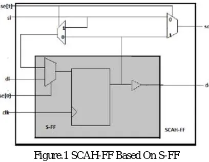
The key element of the single cycle access structure with hold mode (SCAhS) is the signal cycle access register(Flip-Flop, FF) with hold mode (SCAh-FF). It is based on a standard scan register (S-FF) and uses two more 2-to-1multiplexers.
Figure.1 SCAH-FF Based On S-FF
The inputs clock {clk}, data-in {di}, and scan-in {si} still exists. The scan-enable is now a 2 bit bus {se[0:1]}. An additional scan output pin {so} is added. The reset input and inverse output pins are not shown is best explained by a truth table in Table I.
Table I. Truth Table Of SCAh-FF
se[0:1] do@clk So Mode
00 Di Si Functional
01 Di Do Asyn, read
10 do, unchanged Si Hold
11 Si Do Syn,read&wri
The internal logic enables the register to run in one additional hold mode, whereas the additional output multiplexer can bypass the register to directly drive the value of {si}. The resulting functionality ,in functional mode {se[0:1]==00} , the register captures {di} and {si } follows {so } (usually stable). In read mode{ so } has the value of {do} so that {do} can be read out asynchronously. In the event of the relevant clock edge, the register captures {di }.In hold mode, { so } follows {si }, and the register remains in the state {do}, capturing its own value. When{se[0:1]==11} , the registers captures { si} and {so } changes to the new value of {do } (sync. write/read mode).The slave latch of a FF is usually connected to the output driver of the data-out pin and/or an inverting driver for the inverse-data-out pin.
The internal multiplexer for the SCAh-FF (shown in Figure 1) can also be driven by this slave latch output. The fan-out number of the data-out pin (or inverse-data-out pin) refers to the number of input pins which are driven by the SCAh-FF data output drivers.
B.SCAH-STRUCTURE WITHOUT HOLD MODE
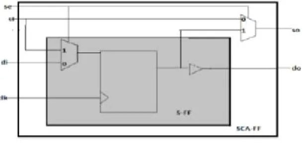
In order to reduce the area overhead of a SCAhS, a simpler SCA-FF is discussed. It adds only one 2-to-1 MUX to the standard S-FF (figure.1). It only has one input, which is connected to the individual line-select signal. The pin which is connected to the global enable signal in the SCAhS is removed, so that the complete global scan enable tree becomes obsolete. The SCA-structure (SCAS) connectivity and page organization equals the one of the SCAhS without the global scan enable {se }.
The key element of the single cycle access structure without hold mode (SCAhS) is the signal cycle access register(Flip-Flop, FF) without hold mode (SCAh-FF). It is based on a standard scan register (S-FF) and uses one more 2-to-1 multiplexer. The new SCA-FF can be seen in Figure 2.
Table II Truth Table Of SCA-FF
Se do@clk So Mode
0 Di Si Functional
1 Si Do syn,read&wri
The SCA-FF has one more input and one more output compared to the standard shift register (S-FF). The inputs clock {clk}, data-in {di}, and scan-in {si} still exists. The scan-enable is now single bit {se}. An additional scan output pin {so} is added. The reset input and inverse output pins are not shown. The additional output multiplexer can bypass the register to directly drive the value of {si}.
Figure 2.SCA-FF Based On S-FF
The resulting functionality is best explained by a truth table in Table II. Thus additional one multiplexer in single cycle access without hold mode will effectively test the scan cell in a single cycle and it reduces the area consumption as compared to single cycle access with hold mode .Also it reduces the test access time(TAT).
III. EXPERIMENTAL DETAILS
A.COMPARISON WITH DIFFERENT TECHNIQUES
Based on the difference in scanning ,the time taken to generate output will vary. Based on this, the detection of target faults may delayed. In the already existing technique such as scan and shift method each of the bit is shifted through the registers one by one. Figure 3. shows the comparison logic of different methods.
Initially sequential circuit testing is done by dynamic shift method ,here each of the flip flop is considered as scan flip flop at the time of scanning. During normal mode of operation the circuit works along with the input and produce functional operations. Here the shifting is dynamic in nature. That is divide the entire scan chain into number of segments and the scan input is loaded to the registers in segment wise.
The variations in with hold and without hold mode cause a difference in area utilization. Similarly all these techniques compare with the normal shift scan method and obtain the variations in fault cover report , area utilization and clock cycles used.
Figure 3 Comparison circuit
IV.RESULT AND DISCUSSION
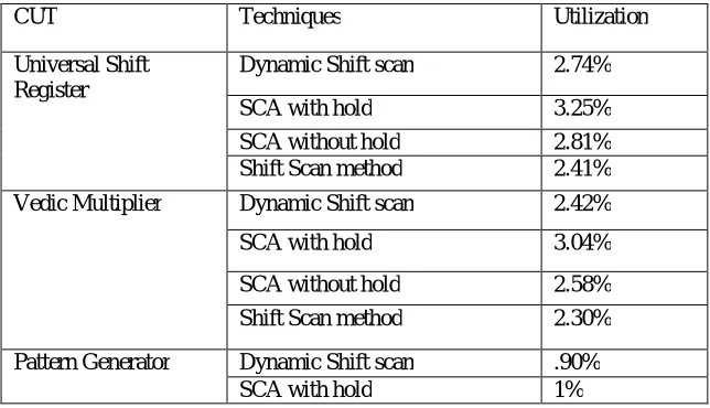
The comparison for the different sequential circuit testing methods are included in the Table III.Here the area utilization of different methods using different CUT’s are compared. It is clear that ,for single cycle access with hold mode the area utilization is high as compared to other methods.
Table III Area Utilization of Different Techniques
In Single Cycle Access with hold mode all the flip flops are tested simultaneously. Figure 4.9 shows the testing of 8 bit universal shift register using single cycle access with hold mode. In Single Cycle Access without hold mode the scan flip flops are converted to a scan flip flop with additional one 2:1 multiplexer. It won’ give the holding operation of the flip flops. Due to the single cycle access method all the faults present in the circuit will detect within a single cycle. Instead of testing the memory elements in a scan chain ,here all the flip flops are tested simultaneously. Therefore in a single clock cycle itself fault report will complete
CUT Techniques Utilization
Universal Shift Register
Dynamic Shift scan 2.74%
SCA with hold 3.25%
SCA without hold 2.81%
Shift Scan method 2.41%
Vedic Multiplier Dynamic Shift scan 2.42%
SCA with hold 3.04%
SCA without hold 2.58%
Shift Scan method 2.30%
Pattern Generator Dynamic Shift scan .90%
Figure 4. Single Cycle Access without hold mode in 8 bit Universal Shift Register .
This will increase the area consumption due to additional one 2:1 multiplexer but it reduces the time consumption to a single cycle. As compared to single cycle access with hold mode it reduces the area consumption.
V. CONCLUDING REMARKS
This paper presents a modification to reduce the test access time ,that is single cycle access with hold mode. Instead of a long scan chain ,if each of the scan cells are tested separately in a single clock will reduce the access time and hence the effective testing time of sequential circuits.If single cycle access with hold mode is used, with the addition of two 2:1 multiplexer in each scan cell ,at a single cycle itself any of the scan cell can be tested. If single cycle access with hold mode is used, with the addition of two 2:1 multiplexer in each scan cell ,at a single cycle itself any of the scan cell can be tested. It may cause some additional area consumption. The effective area utilization can be again reduced by using single cycle access without hold mode. Here additional one 2:1 multiplexer is used in each scan cell and at a single clock cycle itself any of the flip flop can be tested. Therefore the test access time can be reduced and any of the scan cells can be tested in a single clock cycle itself.
REFERENCES
[1] A. Chandra and K.Chakrabarty , “Test Data Compresion and Test Resource Partitioning for System-on-Chip Using Frequency- Directed Run-Length(FDR) Codes ,”in Trans. on Comp., vol. 52, Aug. 2003, pp. 1076-1088.
[2] B.Koenemman ,”LFSR Coded Test Patterns For Scan Design, “ in Pro European Test Conf ., 1991 ,pp 237-247.
[3] I. Pomeranz and S. M. Reddy, “On reset based functional broadside tests,” in Proc. Design Autom. Test Euro. Conf., 2010, pp. 1438–1443. [4] F. Hsu, K. Butler , and J. Patel “A Case Study On The Implementation of the Illinois Scan Architecture, “ Proc. Intl.Test Conf., 2001, pp.
538-547.
[5] J. Rajski et al., “Embedded Deterministic Test,” in Trans. on CAD, vol. 23, May 2004, pp. 776-792.
[6] Polian and F. Fujiwara, “Functional constraints vs. test compression in scan-based delay testing,” in Proc. Design, Autom. Test Euro. Conf., 2006, pp. 1–6.
[7] C.V. Krishna et al., “Reducing Test Data Volume Using LFSR Reseeding with Seed Compression,” in ITC, 2003, pp.321-330. [8] Xijiang Lin and Mark Kassab,” Using Dynamic Shift to Reduce Test Data Volume in High-Compression Designs” IEEE European Test
Symposium (ETS), 2014.
BIOGRAPHY
Ancy Joy was born in India, on September 04, 1991. She graduated from Rajagiri school of engineering & technology,Cochin, Kerala, India in Electronics & Communication Engineering (2013). She completed her Master of Technology in VLSI and Embedded Systems from Viswajyothi College of Engineering and Technology, Ernakulam, kerala, India. Her special fields of interest include VLSI and Embedded System Design.Currently working as assistant professor in Sahrdaya College of Engineering and Technology ,Trissur