ISSN 2348 – 7968
Design Optical Comparator Prototype for
Interferometery
Wail Yas Nassir
Department of Laser and Optoelectronics Engineering, University of Technology Baghdad, Iraq
Abstract
The objective of this research is to design and build a laser comparator prototype that can be utilized in laboratories. The necessity of comparing two laser signals, in suit, in some optical experiments such as holography, interferometer, beam splitting, polarization and sun sensors, to mention but a few, has inspired the researcher to excite the project.
The system under investigation consists of four main electronic circuits: the laser comparator electronic circuit, sign detector and phase inverting circuit and an analog-to- digital readout display circuit.
The comparator has two detectors each receives a particular input signal. Two input signals will be compared and the output will be displayed on a digital readout (or on an oscilloscope). Power difference up to 0.1mW is achieved. Two modulated laser signals are also compared. In general, results are encouraging and promising.
Keywords
: comparator, operation amplifier, detector1.
Introduction
A comparator, by definition is “a circuit that compares two analog input signals and decodes the difference into a single digital output signal”, where out is the single digital output as a result of comparison of two analog inputs In1 and In2. [1]
A comparator has low offset, high gain, and high common-mode rejection. A comparator has a logic output that indicates which of the two inputs is at a higher potential. Comparators are designed to work as open-loop systems, to drive logic circuits, and to work at high speed, even when overdriven [1].
Modern applications for comparators require low current consumption, small packages, and (in some cases) a shutdown function. The modern comparators, for example, work with voltages from 1.6V or 1.8V to 5.5V. [2]
To prevent undesirable output oscillation, a small hysteresis of a few mill volts is integrated into many modern comparators. For comparators without hysterics, the voltage difference between the inputs needed to switch the comparator is the offset voltage, rather than the zero voltage required by an ideal comparator [3].
Depending on the nature, functionality and inputs, comparators are classified into different types i.e. voltage and current comparators, continuous and discrete time comparators etc. Some basic applications of comparators are (ADC), function generation, signal detection and neural networks etc. [3]
2.
Theory
the basic theory needed to understand the fundamental parts in laser comparator design includes the operational concepts of operational amplifier and associated circuits and the comparator and its performance and application.
2.1. Photo-Detector Parameters
ISSN 2348 – 7968
2.2. Comparator
Comparator ICs are designed to compare the voltages that appear at their inputs and to output a voltage representing the sign of the net difference between them. In a comparator circuit, if the differential input voltage is higher than the input offset voltage, plus the required overdrive, the output swings to a voltage representing logic 1. In effect, a comparator can be thought of as a one-bit analog-to-digital converter. [5]
2.3. Comparator ICs
Special comparator ICs are available they are better for joining the analog and digital worlds. They provide a logic state output that indicates the relative state of two analog voltage, one of which is often a fixed reference . Comparators can signal when a voltage exceeds a reference, when a voltage is less than a reference, or when a voltage is whir is a specified range. Comparator ICs must change output state rapidly. They are optimized for high gain, wide bandwidth, and a fast slew rate. [6]
2.4. Comparator Operation
The following drawing, Figure (1 (circuits A and B)) shows the two simplest configurations for voltage comparators. The diagrams below the circuits give the output results in a graphical form as shown in Figure (1 ( a , b )).
Figure 1. Basic Comparator Operation. [7]
For these circuits the reference voltage is fixed at on/e-half of the supply voltage while the input voltage is variable from zero to the supply voltage.
In theory the reference and input voltages can be anywhere between zero and the supply voltage but there are practical limitations on the actual range depending on the particular device used. [7]
2.5. Comparator Input and Output Results
Figure (2) shows the comparator input (a, b) and output (c, d) results. Current will flow through the open collector when the voltage at the plus input is lower than the voltage at the minus input.
ISSN 2348 – 7968
Figure 2. Comparator Input and Output Results. [7]
3.
Design, Construction and Testing the System
The two detectors D1 and D2 form the two input sensors for laser comparator electronic circuit part (1) .It consists of three stages A, B and C. The circuit diagram is shown in Figure (3).
B
C A
R5 100k
R4 100k
R3 100k Q2 NPN
Q1 PNP
Vo +
UC LM324
R2 1k R1 1k
+ UB LM324 +
U1 LM324
+ V2 6V + V1 6V
D2 D1
Figure 3. Electronic circuit of laser Comparator.
4.
Result and discussion
This section is dedicated to evaluate the performance of the laser comparator under consideration. Results regarding DC electric signals, CW laser and modulated laser signals are demonstrated and discussed.
For comparison reason, it is decided to test the system first by receiving the output signal directly on an oscilloscope, then on an analog to digital converter circuit. Below are steps that have been followed.
4.1. Two DC Input Signals
ISSN 2348 – 7968
Table 1. Demonstrates results of comparing two input electrical DC signals. Vout
DC input (V2) DC input (V1)
6 0.5
1
-6 1.5
1
Zero 2
2
-6 2.1
2
-6 4
2
6 2
3
4.2. Two CW Laser Signals
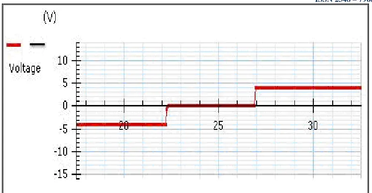
Again, to get a rather quick impression of how the comparator functions the output of the electronic circuit is directly applied to an oscilloscope. Figure (4) displays three outputs, (a) when P1> P2, (b) when P1=P2 and (c) for P1<P2. Where P1 and P2 are input powers to detectors D1 and D2.
(a) (b) (c) Figure (4) Displays comparator output signals , (a) +6V (P1> P2),
(b) 0V(P1= P2), (c) -6V (P1<P2). Scale is (5V/div).
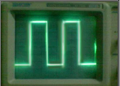
4.3. Comparison between Two Laser Signals of Different Frequencies:
Two different laser frequencies (of equal intensities) can be obtained by letting two laser beams to pass through the fan at different position from the center of the fan blades. Detectors D1 and D2 are allowed to receive the laser signal. An oscilloscope is employed to display the output profile. Figure (5) display the output waveform when two equal frequencies (FD1=FD2) are compared.
ISSN 2348 – 7968
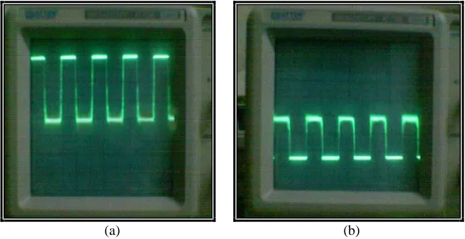
Figure (6 (a & b)) illustrates the output waveform when FD1 > FD2 (located at the positive side) and FD1 < FD2 (located at the negative side) respectively, where FD1 and FD2 represent frequencies received by detectors D1 and D2.
(a) (b)
Figure 6. (a) The output pulse waveform (in positive) when FD1 > FD2. (b) The output pulse waveform (in negative) when FD1 < FD2.
5.
Conclusion
New laser comparator device based on compare between two input laser signals with difference values of powers. The device design can help to solve the problems in experiment work which required measure the difference between two laser signals.
In op-amps and comparators rules the output of these ICs becomes in two cases, positive or negative. The laser comparator device is proved this basic rules in it performance. The results show that the
difference in power between two input laser signals. Where if the fixed power in first detector (D1) is higher than the varying input powers in second detector (D2), then the output is positive.
If the varying input powers in first detector (D1) is lower than the fixed power in second detector (D2), then the output is negative.
6.
Computer Simulation Results
Referring to Figure (7), results of employing different light intensities (or voltages) (Vs) upon sun sensors (1) and (2) are illustrated in Table (2), where 6V supply voltage is used. The performance of this simulation has shown an agreement with the performance of the comparator under consideration. Figure (7) indicates this remark, where the output equals zero for equal input intensities and positive values when V1>V2 and negative values when V1<V2.
Table 2. Demonstrates results of comparing two input sun sensors.
The output (Vout) Light sun sensor (V2)
Light sun sensor (V1)
1.06 0
1.06
-1.06 1.06
0
Zero 1.06
1.06
-5 3.03
2.04
5 2.04
ISSN 2348 – 7968
Figure 7. Output of computer simulated comparator.
7.
References
[1] A .Sher ,“Design of high –speed CMOS comparator” , Master Thesis in Electronics System at Linköping Institute of Technology, 2007.
[2] Maxim Integrated Product, “Amplifier and Comparator circuits”, ECN Magazine App Notes 886, Lab, 2001.
[3] A. Rodriguez.V, F. Medeiro, “Comparators” , University of sevilla, spain, CAM, 1985.
[4] Module 4 ; “ photo detectors characteristics ” ;
TUhttp://cord.org/cm/leot/Module4/module4.htm April 23.2001UTH.
[5] R. Moghin, “Curing Comparator Instability with Hysteresis” , Analog dialogue, 34-07, Lab,2002.
[6] D.J. Daily , “Operational Amplifier and Linear Integrated” , Theory and applications, ch7, P 239-243, 1997.
![Figure 1. Basic Comparator Operation. [7] For these circuits the reference voltage is fixed at on/e-half of the supply voltage while the input voltage is](https://thumb-us.123doks.com/thumbv2/123dok_us/7829082.1297310/2.612.142.485.304.542/figure-comparator-operation-circuits-reference-voltage-voltage-voltage.webp)
![Figure 2. Comparator Input and Output Results. [7]](https://thumb-us.123doks.com/thumbv2/123dok_us/7829082.1297310/3.612.135.494.334.540/figure-comparator-input-output-results.webp)