Optimization Techniques for Low Power VLSI
Design
Abstract- With shrinking technology, as power density (measured in watts per square millimetre) is raising at an alarming rate, power management is becoming an important aspect for almost every category of design and application. Reducing power consumption and over all on chip power management are the key challenges in deep sub micro meter nodes due to increased complexity.
Power management needs to be considered at very early design stages. Also low-power techniques should to be employed at every design stage, from RTL (Register Transfer Level) to GDSII. This survey paper describes the various strategies, methodologies and power management techniques for low power VLSI circuits. Future challenges that must be met by designers to designs low power high performance circuits are also discussed. State-of-the-art optimization methods at different abstraction levels that target design of low power digital VLSI circuits are surveyed.
Keywords— Optimization, low power, power dissipation, power management
I. INTRODUCTION
In the past decades, the main focus of VLSI designers were performance, area and design cost. Power consumption was mostly of on ly secondary importance relatively. However, this trend has begun to change and, with major priority, power consumption is given co mparable impo rtance to speed and area.
The advantage of utilizing combination of lo w-power design techniques in conjunction with low-power co mponents is more valuable now. Heat generation in high-end co mputer
office noise diminishes with low power VLSI chipset. Requirements for lo wer power consumption continue to increase significantly as co mponents become battery-powered, compact and require co mplex functionality. At sub micro meter process nodes, leakage power consumption has joined switching activity as a primary power management concern.
II. RELATED CONCEPTS A. Power Dissipation Basics
Total power consumption by a CMOS device is given by, Pdissipation = Pstatic + Pdynamic + Pshort circuit... (a) Dynamic power or switching power is power dissipated during charging or discharging of capacitors and is described below [1] [2].
Pdyn = CL* Vdd2 *α * f ... (b)
Where CL : Load Capacitance is a function of fan-out, wirelength, and transistor size,
Vdd : Supply Vo ltage, which has been dropping with successive process nodes,
α: Activity Factor
f :Clock Frequency, which is increasing at each successive process node.
Short-circu it power d issipation occurs due to short circuit current(Isc) that flo ws when both the NMOS and PM OS devices are simultaneously ‘on’ for a short time duration and
Kavya R
PG Student [VLSI Design and Embeded Systems], Dept. of ECE, Sri Jayachamarajendra College of Engineering,
Mys uru, Karnataka, India
Dr. S.Gayat
h
ri
Associate Professor, Dept. of ECE
Static power d issipation is due to reverse saturation, sub -threshold and leakage current and occurs especially when the device is in idle mode. It is given by the below equation. Pstatic = f(Vdd , Vth, W/L) ...(d)
Figure 1: Power Dissipation in CMOS
where Vth is threshold voltage, ‘W’ is transistor width and ‘L’ is transistor length
Figure-1 shows the various components responsible for power dissipation in CMOS.
B. Low Power Strategies
Low power designs strategies at various abstraction levels are listed in table 1.
Effective power management is possible by using the different strategies at various levels in VLSI Design process. So designers need an intelligent approach for optimizing power consumptions in designs.
C. Power Optimization Techniques
Table-2 describes low power techniques used at different levels [3][4].
Table 2: Few low power techniques used today
III. POWER MANAGMENT STRAGTEGIES Effective power management involves selection of the right technology, the use of optimized libraries, IP (intellectual property), and design methodology [3].We survey state-of-art optimization methods at different abstraction levels.
Inventory Management), POS (Point of Service), ReSA (Retail Sales Audit) and RIB (Retail Integration Bus).
A. Technology Level
Proper technology selection is one of the key aspects of power management [3]. The goal of each technology advancement is to improve performance, density, and power consumption more generalized form of scaling is used.
i. Using Multi-threshold Voltage
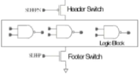
Multi-threshold CM OS (MTCM OS)is a method to reduce standby leakage current in the circuit, with the use of a h igh threshold apply to the MOS device to de- couple the logic either fro m the supply or ground during long idle periods, or sleep states. The Figure 2 shows a MTCMOS circuit, where the logic block is constructed using low threshold devices and the Power/ground supply given to the gate of the of the MTCOMS is a gated by high threshold header/footer switch[5].
ii. Multi-supply Voltage (Voltage Islands)
Multi-Vdd is an effective method to reduce both leakage and dynamic power, by assigning different supply voltages to cells according to their timing criticality. In a multi-Vdd design, cells of different supply voltage are o ften grouped into small number of voltage islands (each having a single supply voltage), in order to avoid co mplex power supply system and excessive
amount of level shifters. Low power design
methodology which manages power, timing and design
cost by using multi-Vdd and voltage islands has to be
developed [5] [6].
iii. Dynamic Voltage and Frequency Scaling
It allows host to dynamically switch its CPU frequency depending on its load requirement. CPU utilization is continuously monitored with the DVFS algorith m determin ing any necessary adjustment to the CPU’s frequency with the goal being to run the CPU at a lo wer frequency so that it consumes less power. Examp le: If 2 GHz CPU is sitting at 30% utilization then DVFS will reduce the frequency of the CPU so it will operate nearer to its 600M Hz frequency requirement including enough headroom to accommodate a sudden increase in CPU requirement[7][8][9][10].
B. Circuit Level
Transistor Sizing: The length-to-width ratio of transistors determines the driving strength and speed.On upsizing, gate delay decreases, however, power d issipated in the gate increases. Further, the delay of the fanin gates increases because of increased load capacitance. Given a delay constraint, finding an appropriate sizing of transistors that minimizes power dissipation is a computationally d ifficult problem. A typical approach to the problem is to compute the slack at each gate in the circuit, where the slack of a gate corresponds to how much the gate can be slowed down without affecting the critical delay of the circuit.
C. Logic Level
We survey optimizations that reduce switching activity power of logic-level co mbinational and sequential circu its in- this section.
i. Combinational
Co mbinational logic optimization has traditionally been decomposed into two phases: technology-independent optimization and technology-dependent optimization. In the first phase logic equa- tions are manipulated to reduce area, delay or power d issipation. In the second phase the equations are mapped to a particular technology library using technology mapping algorith ms, again optimizing for area, delay or power. Fo r a co mprehensive treatment of combinational logic synthesis methods targeting area and delay [11].
Don’t-care Optimization: Any gate in a comb inational circuit has an associated controllability and observability don’t-care set. The controllability don’t-care set corresponds to the input combinations that never occur at the gate inputs. The observability don’t-care set corresponds to collections of input combinations that produce the same values at the circuit outputs. Methods to reduce circuit area and imp rove delay exploiting don’t- care sets have been presented in [12]. The power dissipation of a gate is dependent on the probability of the gate evaluating to a 1 or a 0. This probability can be changed by utilizing the care sets. A method of don’t-care optimization to reduce switching activ ity and therefore power dissipation was presented in [13]. This method was improved upon in [14] where the effect of don’t-care optimization of a particu lar gate on the gates in its transitive fanout is considered.
Path Balancing: The delays of paths that converge at each gate in the circu it should be nearly equal to reduce spurious switching activity. By selectively adding unit-delay buffers to the inputs of gates in a circuit, the delays of all paths in the circuit can be made equal. Th is addition will not increase the critical delay of the circu it, and will effectively eliminate spurious transitions. However, the addition of buffers increases capacitance which may offset the reduction in switching activity. Design of a mu ltiplier with transition reduction circuitry that acco mplishes glitch reduction by path balancing is described in [15].
Factorization: Factorization of logical exp ressions is primary means of technology-independent optimization. Examp le, the expression ac + ad + bc + bd can be factored into (a + b) (c + d) reducing transistor count considerably. Modified kernel extraction methods that target switching activity power are described in [16].
Optimized logic equations are mapped into a target library that contains optimized logic -gates in the chosen technology. A typical lib rary will contain hundreds of gates with different transistor sizes. Modern technology mapping methods use a graph covering formulation, orig inally presented in [17], to target area and delay cost functions. The graph covering formulation of [17] has been extended to the power cost function.
iii. Sequential
Encoding State encoding for minimal area is a well-researched problem [18]. These methods have to be modified to target a power cost function, namely, weighted switching activity. Methods to encode State Transition Graphs to produce two-level and multitwo-level implementations with minimal power are described in [16] and[19]. Encoding to reduce switching activity in datapath logic has also been the subject of attention. A method to min imize the switching on buses is proposed in [20].
Retiming: Retiming [21] is a well-known optimization method that repositions the flip-flops in a synchronous sequential circuit so as to minimize the required clock period. A retiming method that targets the power dissipation of a sequential circuit is described in [22].
Clock Tree Optimization and Clock Gating: Rapid scaling has two profound impacts. First, it enables much higher degree of on-chip integration. The number of transistors per chip will increase by more than 2x per generation according to Moore's law. Second, Interconnect has become the dominating factor in determining circuit performance and reliability in deep submicron designs. The interconnect design will play the most critical role in achieving the projected clock frequencies Clock distribution is crucial for timing and design convergence. Minimu m delay/power, zero skew buffer insertion/ sizing and wire-sizing problems have long been considered intractable .Most of the power is consumed due to the high clock frequency used for operating the device. Portions of the clock tree that are not being used at any particular time can be disabled to save the power.
iv. Pin Swapping
Some cells can have input pins that are symmetric with respect to the logic function (for example, in a 2-input NA ND gate the two input pins are symmetric), but have different capacitance values. Power can be reduced by assigning a higher switching rate net to a lower capacitance pin
Power minimization techniques like p in swapping is also called as local transformations [23]. They are applied on gate netlists, and focus on nets with large switched capacitance. Example: Consider 4 input NAND gate with different capacitance value at the pin as show in the Figure 3. a h igh activity net is connected to the pin no 4 that is pin “d” which has the min imu m input capacitance. To achieve the min imu m input capacitance pin swapping is done between the pins “a” and “d”.
v. Power Shutoff or Power Gating
Power gating is the technique used to temporarily turn off the sub blocks to reduce the overall leakage power o f the chip. This temporary shutdown time can also call as “low power mode” or “inactive mode”. When circuit blocks are required for operation once again they are activated to “active mode". These two modes are switched at the appropriate time and in the suitable manner to maximize power performance wh ile minimizing impact to perfo rmance. Thus goal of power gating is to minimize leakage power by temporarily cutting power off to selective blocks that are not required in that mode.
D. Architectural and Behavioural level
i. Memory Splitting
Off-chip memory accesses are very expensive power wise. Reordering of bus transactions (to minimize signal transitions) can reduce overall energy consumption. Nu mber of b it flips on the memory bus can be reduced by proper data encoding or by scheduling bus transactions in the order in wh ich they would cause the minimal signal changes.
ii. Operand Isolation
Redundant operations are identified and special isolation circuitry is used to prevent switching activity fro m propagating into a module whenever it is about to perform a redundant operation.
An increasing fraction of applications are being imp lemented as embedded systems consisting of a hardware and a software components. As major part of the functionality is in the form of instructions as opposed to gates, Hardware-based power estimation and optimization approaches are not co mpletely applicable here. Th is motivates the need to consider the power consumption in micro- processors from the point of view of software. Instruction-level power models are developed successfully for some co mmercial CPUs. Given the ability to evaluate programs in terms of power/energy costs, it is possible to search the design space in software power optimization. The choice of the algorithm used can impact the power cost since it determines the runtime comp lexity of a program. This issue is explored in [24]. It has been noted that the order of instructions can also have an impact on power since it determines the internal switching in the CPU.
CAD Methodologies and Technique: Today's EDA tools effectively support these power- management techniques [25]. They also provide additional power savings during implementation. Lo w power VLSI designs can be achieved at various levels of the design abstraction fro m algorith mic and system levels down to layout and circuit levels.
IV. CONCLUSION
High power consumption not only leads to short battery life for hand-held devices but also causes on-chip thermal and reliability problems in general. The need for lo wer power systems is being driven by many market segments. As application demands increase toward mo re power sensitive devices, new and novel approaches are needed to meet those demands. Several of these techniques can be used in unison to provide the lowest power solution possible. Sleep mode, clock gating, power gating, gate level optimizations, low power libraries, low power arch itectures and voltage scaling are all proven lo w power techniques and should be considered when architecting any new application. Designing for low power adds another dimension to the already complex design problem; the design has to be optimized for Power as well as Performance and Area. Optimizing the three axes necessitates a new class of power conscious CAD tools.
We have surveyed power optimizations applicable at various levels of abstraction, Lowering power diss ipation at all abstraction levels is a focus of intense academic and industrial research. These methods are being incorporated into state-of-the-art Computer-Aided Design frameworks.
REFERENCES
[1] Shekar Borkar, "Design Challenges of Technology Scaling," IEEE Micro , July/August 1999, pg 23. [2] T. Inukai, et.al, “Boosted Gate M OS (BGM OS):
Device/Circuit Cooperation Scheme to Achieve Leakage- Free Giga- Scale Integration,” Proc. CICC 2000, pp.409-412.
[3] Michael Keating, David Flynn, Robert Aitken, Ala Gibsons and Kaijian Shi, “Lo w Power Methodology Manual for System on Ch ip Design”, Springer Publications, New York, 2007. [4] Creating Low-Power Digital Integrated Circuits The
Implementation Phase, Cadence, 2007.
[5] C. Chen and M. Sarrafzadeh “A Efficient Algorithm for Gate Level Power Delay Trade of using Two Vo ltages”, International Conference on Co mputer Design, pp. 222-227, October 1999.
[6] J.M. Cheng and M. Pedram “Energy M inimization using Multi Supply Vo ltage”, IEEE Transaction on VLSI System, Vol. 5, No. 4, pp. 1-8, December 1992.
[7] Qqiang M Q and Evangeline, “Vo ltage island-Driven Floor Planning”, Proceeding of IEEE, pp. 644-649, 2007.
[8] P. J. Shah, P.P atil, V.M. Deshmukh and P. H. Zope, “Low Power VLSI Design using Dynamic Thershold logic”, Proceedings of SPIT-IEEE Colloquium International Conference Mumbai, Vol. 2, pp. 121. [9] Wong, M.D.F., “Low Power Design with Mu lti-Vdd and
Vo ltage Islands”, ASIC ASICON ‘07, 7th International Conference, pp. 1325-1325, 2007.
[10] Li Shang, Li-Shiuan Peh, Niraj K. Jha, “Dynamic Vo ltage Scaling with Lin ks for Power Optimization of Inter- connection Networks”, The Ninth International Symposiu m on High-Performance Co mputer Architecture, HPCA-9 2003, Proceedings, pp. 91-102, ISSN: 1530-0897, 12 February 2003.
[11] S.Devadas, A.Ghosh, andK.Keutzer. LogicSynthesis. McGraw Hill, New York, NY, 1994.
[12] H. Savoj, R. Brayton, and H. Touati. Extracting Local Don’t- Cares for Netwo rk Optimization. In Proceedings of the Interna- tional Conference on Computer-Aided Design, pages 514–517, November 1991.
[13] A. Shen, S. Devadas, A. Ghosh, and K. Keutzer. On Average Power Dissipation and Rando m Pattern Testability of Co mb ina- tional Log ic Circuits. In Proceedings of the Int’l Conference on Co mputer-Aided Design, pages 402–407, November 1992.
[14] S. Iman and M. Pedram. Multi-Level Network Optimization for Lo wPo wer. InProceedingsoftheInt’lConferenceonComputer- Aided Design, pages 371–377, November 1994.
[16] K. Roy and S. Prasad. SYCLOP: Synthesis of CMOS Logic for Low Power Applications. In Proceedings of the Int’l Conference on Co mputer Design: VLSI in Co mputers and Processors, pages 464– 467, October 1992.
[17] K.Keutzer. DA GON:Technology Mapping andLocalOptimiza - tion. In Proceedings of the 24th Design Automation Conference, pages 341–347, June 1987.
[18] P. Ashar, S. Devadas, and A. R. Newton. Sequential Logic Synthesis. KluwerAcademic Publishers,Boston, Massachusetts, 1991.
[19] C-Y. Tsui, M. Pedram, C-A. Chen, and A. M. Despain. Low Po wer State Assignment Targeting Two - and Multi-level Logic Implementations. In Proceedings of the Int’l Conference on Co mputer-Aided Design, pages 82–87, November 1994.
[20] M. Stan and W. Burleson. Limited-weight codes for low-power I/O. In Proceedings of the Int’l Workshop on Low Power Design, pages 209–214, April 1994.
[21] C. E. Leiserson, F. M. Rose, and J. B. Saxe. Optimizing Syn- chronous Circuitry by Retiming. In Proceedings of 3rd CalTech Conference on VLSI, pages 23– 36, March 1983.
[22] J. Monteiro, S. Devadas, and A. Ghosh. Retiming Sequential Circu its for Low Power. In Proceedings of the Int’l Conference on Co mputer-Aided Design, pages 398–402, November 1993.
[23] Seongmoo Heo and Krste Asanovi, “Dynamically Resizable Static CM OS Logic for Fine-Grain Leakage Reduction”, MIT CSAIL Technical Report (MIT-LCS-TR-957), July 2004.
[24] P. w. Ong and R. H. Yan. Power-conscious software design - a framework fo r modeling software on hardware. In Proceedings of 1994 IEEE Sy mposium on Low Power Electronics, pages 36– 37, San Diego, CA, Oct. 1994.