IJEDR1603145
International Journal of Engineering Development and Research (www.ijedr.org)898
Design of High Speed, Low Power and Wide range
Ripple Detector for On-Chip testing in CMOS
Technology
1
T.Vasudha,
2Dr. S.P. Venu Madhava Rao
1PG Scholar,2Head Of the Department
1,2Department of Electronics and Communication Engineering 1,2Sreenidhi Institute of Science and Technology, Hyderabad,India
________________________________________________________________________________________________________
Abstract- On chip testing is an attractive solution for testing of analog integrated circuits. In this paper a low power , built in CMOS Ripple Detector is presented for the purpose of detecting the ripples in the supply rails and specifies its application for On chip testing. The detector works on the principle of RMS detection. The circuit outputs a DC signal that is proportional to the peak to peak amplitude of input ripple. The detector can detect a peak to peak ripple voltage in the range of 8mV to 100mV on a 1.2 Volts supply over an operating frequency of 220MHz , and consumes 3mW power. The detection time is reported to be 0.5ns. Implementation of the detector is carried out in 65nm CMOS technology.
Keywords - supply ripple, on chip testing, detection time, low power, power management.
________________________________________________________________________________________________________
I.INTRODUCTION
Power supply that is free from ripple is crucial for all analog and digital circuits in system on chip environment where each of them requires a stable power supply. Ripple is a low frequency component in the power supply's output voltage and is measured as a peak to peak voltage in the order of milli volts range[1]. In fact ,detecting this milli volts ripple in the power supply is a serious challenge. TV receivers show wavy lines if too much ripple is present and in digital integrated circuits presence of ripple causes increase in the clock jitter and incurs a reduction in the noise margin[2]. As this power supply noise degrades the system performance, the fluctuations in the supply rails is a key parameter that should be carefully monitored.
Supply ripple is an important performance measure for Voltage regulators and highly efficient switch mode DC to DC converters [3] ,which form the important building blocks of power management integrated circuits and moreover now the trend is emerging towards voltage regulators which are integrated on chip [4-5] .These integrated voltage regulators, irrespective of their load conditions they provide constant DC voltage, but sometimes vulnerable to process variations that gives rise to ripple in the output voltage and this ripple effects the performance of rest of the circuit. Ripple measurement can be done using can be using external test equipment and probes, but this type of testing the ripples suffers from many draw backs. The impedance of the probes will result errors in the circuit and thus contribute to false measurements. Secondly the increased test times and testing of each block independently in case of off chip testing is time consuming and expensive. So in order to overcome the above problems there is a need for on chip testing solution [6-7]. It is the most economical and accurate solution while testing of complex integrated circuits, the ripple can be measured on chip without the requirement of special probes or other external test equipment[8].
In this work, a low power, high speed and wide range built in ripple detector is proposed in 65nm CMOS technology for the purpose of detecting the ripples present in the supply line and the application of the proposed detector is intended for on chip testing of integrated voltage regulators. The operating frequency of the detector is 220MHZ with 1.2V supply voltage. It senses the peak to peak ripple voltage on the basis of RMS or amplitude detection. Finally, the output of the circuit is a digital high or low level signal indicating the detection of the ripple. The paper is organized as follows:Section2 deals with detectors methodology, implementation of the circuit is described in Section3,simulation results and conclusions are presented in Section4 and 5.
II. METHODOLOGY OF DETECTORS
IJEDR1603145
International Journal of Engineering Development and Research (www.ijedr.org)899
Fig.1Basic Block diagram of CMOS Ripple Detector
The basic idea is to amplify the input ripple which is given to the detector to generate a DC voltage and thereafter this dc signal and reference are given to the comparator. It will output a high level signal indicating the detection of the ripple.
III. CIRCUIT IMPLEMENTATION
i. Amplifier
Amplification forms the initial phase in the ripple detection. There is a need for amplification because a weak signal that is directly fed into the circuit which is not amplified ,will disappear quickly and to overcome the noise of the subsequent stage it is necessary. This block is designed with two single ended differential amplifiers as Single ended operation is preferred for lo w power applications and increasing the number of amplifying stages will improve the detector's sensitivity[16].Differential topology is used as it has the special property of nullifying the noise in the power supply lines. Fig.2 shows the current mirror loaded PMOS differential pair formed by M2 and M3 with input 8mV ripple applied at the gate of M2.Mosfet M1 is a constant current source that provides constant bias current to the differential pair, that means it establishes DC operating point required for the transistor to operate in saturation region. Resistor R1 determines the proportion of the signal that appears at the input of the amplifier.
Current mirror formed by M4and M5, they load the input transistors M2 and M3.The output from the amplifier1 is coupled to amplifier2 through coupling capacitor C2 shown in Fig.3. The amplified signal is obtained at drain of M9.Bulk of PMOS is shorted to its source and connected to VDD while the bulk of NMOS transistor is connected to ground in order to avoid the body effect.
Fig. 2 Differential Amplifier1
Amplifier
Detector
Built in
reference
generator
Comparator
8mVIJEDR1603145
International Journal of Engineering Development and Research (www.ijedr.org)900
Fig. 3 Differential Amplifier2ii. Detector
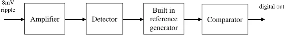
The circuit for the detector is shown in Fig.4.Resisitor R3,Transistor M12 and the capacitor C4 forms the detector. The amplified signal from the amplifier is fed in to the detector through capacitor C3,where the capacitor blocks the DC current from influencing the detector operation. Resistor R3 is used for biasing the gate of the transistor M12 .This arrangement provides high gain when the signal amplitude is low and ensures that the drain current of M12 equals to the bias current. Transistor M11 behaves as a constant current source. The bias current through M12 is given as sum of drain current through M11 and current through R3.Capacitor C4 keeps the drain of M12 at a constant voltage. When the input signal amplitude at the gate of M12 increases, the current at the output node increases ,so M12 discharges the capacitor C4 there by Voltage across Mosfet M12 that is Vds decreases, which means voltage drops proportionally to peak input amplitude[17].
Fig. 4 Single ended detector
iii. Built in reference generator
IJEDR1603145
International Journal of Engineering Development and Research (www.ijedr.org)901
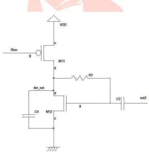
considerations in to account, reference is generated in built without giving any external DC reference. Fig. 5 shows the circuit in that the reference is obtained by reading the output voltage of the detector when no input signal is applied. It is the most simplest and accurate form of generating the reference.Fig. 5. Reference circuit
iv. Comparator
Comparator forms the final stage of the detector.Fig.6 shows the comparator circuit which is build with preamplifier followed by buffer stages. The preamplifier is designed with differential structure because of its better signal swing. Transistors M15,M16 forms the differential pair to which the detector output and reference voltage are given as inputs. The purpose of the preamplifier is to amplify the input signal to improve the comparator sensitivity. Transistors M13,M14 form the cross coupled active load or PMOS latch. This cross coupled structure provides gain multiplication, high voltage sensitivity and strong positive feedback to regenerate the signal.
Fig. 6 Comparator
IJEDR1603145
International Journal of Engineering Development and Research (www.ijedr.org)902
IV. SIMULATION RESULTS
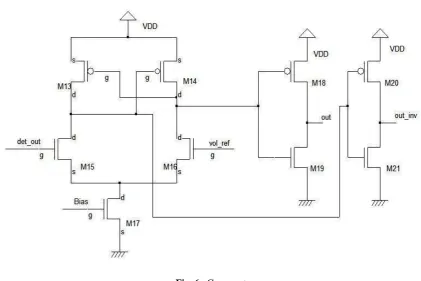
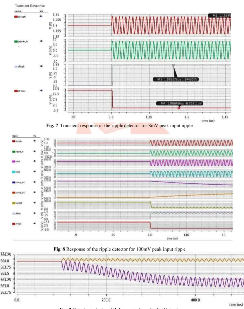
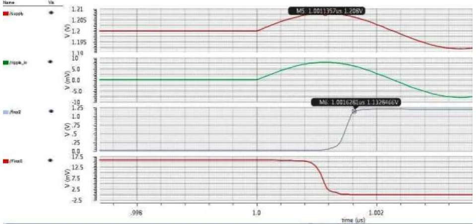
The proposed Ripple detector was implemented and simulated with Cadence Spectre simulator in 65nm CMOS technology. The circuit operates with 1.2V supply voltage and total power consumption is 3mW.Detection range of the detector is reported to be 8mV - 100mV .Fig. 7 and Fig.8 shows transient response of the ripple detector for 8mV and 100mV peak input ripple. Fig. 9 shows the detector output and reference voltage. The detection time(time required to detect the input ripple) which depends on amplification of amplifier chains is found to be 0.5ns shown in Fig.10.
Fig. 7 Transient response of the ripple detector for 8mV peak input ripple
Fig. 8 Response of the ripple detector for 100mV peak input ripple
IJEDR1603145
International Journal of Engineering Development and Research (www.ijedr.org)903
Fig. 10 Settling time of the detector for 8mV peak input rippleV. CONCLUSIONS & FUTURE SCOPE
A low power built in ripple detector is presented to identify the ripples in the power supply. This built in detection system helps to reduce the chip failure and ensures optimal system performance. The minimal area overhead makes it suitable for on chip testing of ripples generated by internal circuits and output voltage ripple of integrated voltage regulators. Moreover, the proposed detector attains good detection accuracy and settling time compared to previous detectors. The faster settling time of the detector proves to be promising for measurement of ripples in fraction of nano seconds. Future research can be can be ex tended in further improving the detection range and obtaining good sensitivity.
REFERENCES
[1] V. Gupta, G.A Rincon Mora,P. Raha,"Analysis and design of monolithic, high PSR,linear regulators for SOC applications",in proc.IEEE international SOC conference, pp.311-315,2004
[2] B. Razavi, "Challenges in the design of high-speed clock and data recovery circuits", IEEE Commun. Mag., vol. 40, no. 8, pp. 94-101, 2002.
[3] J. Guo and K. N. Leung, "A 25mA CMOS LDO with-85dB PSRR at 2.5MHz", in Proc. IEEE Asian Solid-State Circuit Conf., pp. 381-384,2013.
[4] E.A.Burton, "FIVR-Fully Integrated Voltage Regulators on 4th Generation Intel® Core TM SoCs",in Applied Power Electronics Conference and Exposition (APEC), Twenty-Ninth Annual IEEE,pp. 432-439, 2014Y.
[5] S. Dietrich, L. Liao, F. Vanselow, R. Wunderlich and S.Heinen, "A lmV Voltage Ripple 0.97mm2 Fully Integrated Low-Power Hybrid Buck Converter", in IEEE Proc. ESSCIRC 2013, pp. 395-398.
[6] Jee-Youl Ryu, Bruce C. Kim," A New Low-Cost RF Built-In Self-Test Measurement for System-on-Chip Transceivers",IEEE Transactions on Instrumentatiosn and Measurement, vol. 55, no. 2,pp. 381-387, 2006
[7] J. Liobe and M. Margala, "Novel process and temperature-stable, IDD sensor for the BIST design of embedded digital, analog, and mixed signal circuits", IEEE Transactions on Circuits and Systems I: Regular Papers, vol. 54, no. 9, pp. 1900-1915, 2007.
[8] R. Ayadi,M. Masmoudi." A new built in self test for RF Low Noise Amplifier", International Conference on Design and Technology of Integrated Systems in nano scale era(DTIS),pp.1-5,2010.
[9] O. K. Ekekon, S. Maltabas and M. Margala, "Novel programmable built in current sensor for analog digital and mixed signal circuits", in Proc. IEEE Int. Symp. Circuits Syst., pp. 3545-3548
[10] Tao Zhang, William R. Eisenstadt, Robert M. Fox,"20 GHz Bipolar RF RMS Power Detectors", Proceedings of the Bipolar/BiCMOS Circuits and Technology Meeting, 2005.
[11] Q. Yin , W. R. Eisenstadt , R. M. Fox and T. Zhang, "A translinear RMS detector for embedded test of RF ICs", IEEE Trans. onInstrumentation and Measurements., vol. 54, no. 5, pp. 1708-1714, 2005
[12]Seok Bae Park, James E. Wilson, Mohammed Ismail, "The Chip Peak Detectors for Multistandard Wireless Receivers", IEEE Circuits and Devices Magazine, vol 22. no. 6,pp. 6-9, 2006
[13]V. Acharya, S. Cui and B. Banerjee, "On-chip RMS detector using CMOS quad for RF testing",IEEE Silicon Monolithic Integrated Circuits in RF Systems, pp. 1-4, 2009
[14]Alberto Valdes-Garcia, Radhika Venkatasubramanian, Joseilva-Martinez and Edgar Sanchez-Sinencio,"A Broadband CMOS Amplitude Detector for On-Chip RF Measurements",IEEE Transactions on Instrumentation and Measurement,vol.57,no.7.,pp 1471-1477, 2008
[15]Donghoon Han, A. Chatterjee",Robust built in test of RFICs using Envelope detectors",IEEE 14th Asian Test Symposium(ATS'05), pp.2-7, 2005
[16]Adel S. Sedra, Kenneth C. Smith, Microelectronic Circuits,5thed. New york, Oxford universitypress,2008