18 |
P a g e
LOW LEAKAGE POWER BINARY CONTENT
ADDRESSABLE MEMORY CELL
Kiran Kumar M
1, S.L.Gangadharaiah
2 1Student, Department of ECE, M S Ramaiah Institute of Technology, (India)
2
Assistant Professor, Department of ECE, M S Ramaiah Institute of Technology, (India)
Affiliated to Visvesvaraya Technological University, Karnataka(India)
ABSTRACT
Binary content addressable memories are the basic memory cells which are used in network routers, artificial intelligence and neural network applications. These are the memory cells which hold the address of the nodes in routers. Based on the content of the memory cells the operation is performed. Once after the content is written into the memory, it won’t be changed forever. Hence these are used in hold state. And not used in write or read
mode. When the memory cells are not being used in write or read mode they will idle, i.e., just storing the data. At this point of state, the voltage magnitudes need not to be at the perfect levels as the writing into the memory is already done and reading from the memory is not required. Many approaches have been made to reduce the number of transistors in the architecture of these memories but approaches to reduce the power levels when they are in the hold state are very less.
So here is an approach to reduce the power level when they are in hold state. Even though the number of transistors is more compared to the basic content addressable memory architecture, we can achieve the power reduction in the hold state.
Key Words: Content Addressable Memory (CAM).
I. INTRODUCTION
Binary content addressable memories are the cells which are used in the network routers and in many applications. So when we transmit a packet of data which is addressed to reach a particular node, that data packet must have the address of that particular node in the network.
This packet is sent over the network with the help of router and this router would have assigned a particular address to each node and this address of each node is stored in the content addressable memories.
19 |
P a g e
II. MEMORY BLOCKS
Binary content addressable memories are the cells which are used in the network routers and in many applications. So when we transmit a packet of data which is addressed to reach a particular node, that data packet must have the address of that particular node in the network.
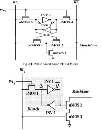
Fig 2.1: NOR based basic 9T CAM cell
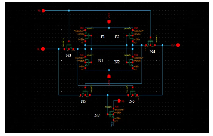
Fig 2.2: NAND based D-Latch 7T CAM cell
20 |
P a g e
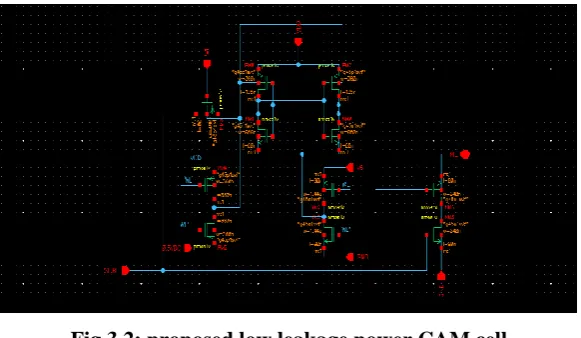
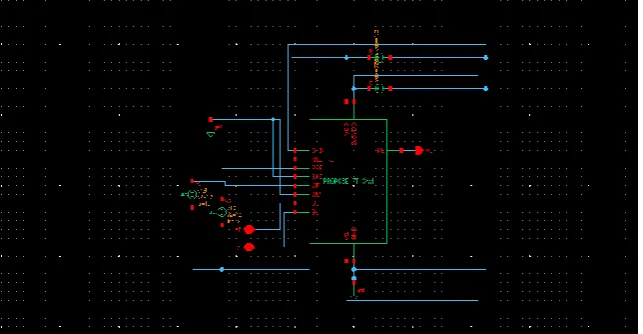
Fig 2.3: proposed design of the low leakage power binary CAM cell
The organization of memory architecture includes the entire sub circuits like pre charge circuit, data enable, match line sense amplifier, memory cell and the match line pre charge transistor. This match line pre charge transistor is a PMOS transistor which is used to pre charge match line exactly like the bit line.
Writing into the memory cell and reading from the memory cell is controlled by the signal WL/WL’ (word line), which enables the pass transistor in the memory cell which can be either NMOS or PMOS.
The proposed design of the binary CAM cell is a pre computation based NAND logic cell. This proposed design not only controls the sub threshold currents but also the gate leakage currents. This will lead to a better reduced static power consuming content addressable memory.
III. DESIGN AND IMPLEMENTATION
21 |
P a g e
Transistor sizes: Let L = 45nm;
For PMOS P1, P2 = (W/L) = (3/3) = (135nm/135nm) = 1; For NMOS N1, N2 = (W/L) = (8/2) = (360nm/90nm) = 4; For NMOS N3, N4 = (W/L) = (12/2) = (540/90nm) = 6; For NMOS N5, N6 = (W/L) = (4/4) = (180nm/180nm) = 1;
Writing Operation: The required datum can be written into the memory with the help of data enable circuit. When the write enable signal “WE” is high the data enable circuit is enabled and the data which we desire to write into the memory is passed through this circuit. At this point of time the signal “WL” signal should be high so that the pass transistors can transfer the data from bit lines to the bistable element. The pass transistors used in this architecture are NMOS (N3 & N4) so these will be enabled when the signal “WL” is high.
Comparison operation: Comparison is the operation which is done when the data is transferred on the search lines and the pass transistors are off. Search lines are nothing but the bit lines itself.
Fig 3.2: proposed low leakage power CAM cell
Design: This architecture uses a D-latch the store the data bit and it’s a pre computation based architecture. Uses NAND logic for comparison of data. The static power such as leakage and sub threshold current is reduced using extra four transistors.
Two NMOS transistors are used to reduce the sub threshold current. When the writing operation is going on the pass transistor should be on that means WL signal should be low as the pass transistor is PMOS, so during this operation the latch should have the proper ground potential so that the bi stability happens and it can store the data, hence N4 (controlled by WL’) will be on and the proper ground potential is provided.
During hold state the data will already be written and there is no need of proper ground potential. When this operation is going on the pass transistor should be off i.e., WL should be high. When WL is high, transistor N3 will be on providing potential which is much higher than the ground potential here Vs=0.6V.
22 |
P a g e
During hold state the data will already be stored in the latch. In hold operation the pass transistor should be off i.e., WL should be high. When WL is high, transistor P5 will be on and all the bulks of the PMOS transistors will get connected to a different potential, which is half of the Vdd that is 0.6V.
So there are totally four extra transistors to reduce this static power. Transistor sizes:
Let L = 45nm;
For PMOS P1, P2 = (W/L) = (3/3) = (135nm/135nm) = 1; For NMOS N1, N2 = (W/L) = (8/2) = (360nm/90nm) = 4; For PMOS P3 = (W/L) = (4/2) = (180nm/90nm) = 2; For NMOS N3, N4 = (W/L) = (12/2) = (540nm/90nm) = 6; For PMOS P4, P5 = (W/L) = (8/3) = (360nm/135nm) = 1; For PMOS N5, N6 = (W/L) = (2/2) = (90nm/90nm) = 1;
Write operation for this memory cell is also same as that of the basic writing operation to the 9T CAM cell. But here this uses a D-latch as storing element, and only one bit line is enough for the writing operation and comparison operation. Here PMOS has been used as pass transistor instead of the NMOS. This architecture uses NAND based logic for the comparison operation.
Input signals: VDD, GND, D_IN, D_IN’, ML_PRE, PRE, SAE, WE, WL, WL’, VS & 0.5VDD. In-Out signals: BL, BL’, ML.
23 |
P a g e
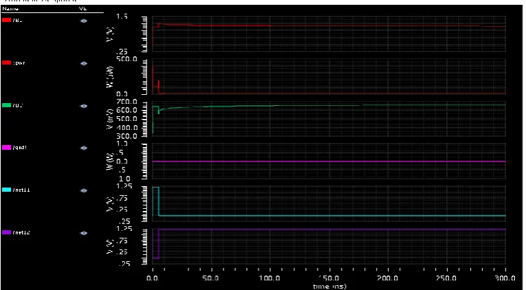
Fig 3.3-b: simulation result of 9T CAM cell for bit 0.
Input signals: VDD=Vdc=1.2V, GND=Gnd, D_IN=0V, D_IN’=1.2V, ML_PRE=0V, PRE=VPulse=300ns (period): 1.2V (5ns) & 0V (295ns), WE =VPulse=300ns (period): 1.2V (5ns) & 0V (295ns), SAE=0V. The simulation set up and results are shown above for 9T CAM cell, writing the data 0 for 5ns and holding it for 295ns resulting in the average power consumption of 107.7uw.
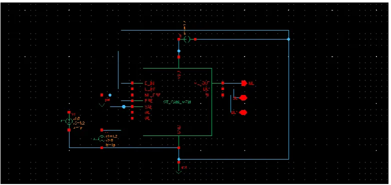
Fig 3.3-c: simulation setup for the test circuit of proposed CAM cell for bit 0.
24 |
P a g e
Input signals: VDD=Vdc=1.2V, GND=Gnd, D_IN=0V, ML_PRE=0V, PRE=VPulse=300ns (period): 1.2V (5ns) & 0V (295ns), WE=VPulse=300ns (period): 1.2V (5ns) & 0V (295ns),SAE=0V, VS=0.6V & 0.5VDD=0.6V.
The simulation set up and results are shown above for proposed CAM cell, writing the data 0 for 5ns and holding it for 295ns resulting in the average power consumption of 86.34uw.
Fig 3.3-e: simulation setup for the test circuit of 9T CAM cell for bit 1.
Fig 3.3-f: simulation result of 9T CAM cell for bit 1.
25 |
P a g e
Fig 3.3-g: simulation setup for the test circuit of proposed CAM cell for bit 1.Fig 3.3-h: simulation result of proposed CAM cell for bit 1.
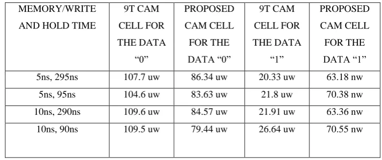
Similarly the power consumption readings has been taken for different writing and holding times and the below table shows the power readings
.
TABLE 1: Average power consumption table of 9T and proposed CAM cell.
MEMORY/WRITE AND HOLD TIME
9T CAM CELL FOR THE DATA
“0”
PROPOSED CAM CELL FOR THE DATA “0”
9T CAM CELL FOR THE DATA
“1”
PROPOSED CAM CELL FOR THE DATA “1” 5ns, 295ns 107.7 uw 86.34 uw 20.33 uw 63.18 nw
26 |
P a g e
The above table shows average power consumptions of 9TCAM cell and proposed CAM cell, for different data bits written and held for different period of time.
IV. CONCLUSION
The average power consumed during writing and hold operation by the proposed content addressable memory is much lesser than compared to that of the basic 9T CAM cell.
Hence it is better to use a pre computation based memory cells when it comes to low power design of VLSI systems. As the technology is improving the power used by these systems has been decreasing rapidly. The key to this kind of system is to make use of low power VLSI design.
REFRENCES
[1] “Practical Implementation of a Low-Power Content-Addressable Memory”, Pedro Echeverr´ıa, Jos´e L.
Ayala, Marisa L´opez-Vallejo,IEEE 2006.
[2] “Variability-Tolerant Binary Content Addressable Memory Cells”, Sheng-Ping Yong, Jin-Fu Li, and
Yu-Jen Huang, 2009 IEEE International Workshop on Memory Technology, Design, and Testing.
[3] “Content-Addressable Memory (CAM) Circuits and Architectures: A Tutorial and Survey”, Kostas
Pagiamtzis, Student Member, IEEE, and Ali Sheikholeslami, Senior Member, IEEE. IEEE JOURNAL OF SOLID-STATE CIRCUITS, VOL. 41, NO. 3, MARCH 2006.
[4] “Design and Analysis of Two Low Power SRAM Cell Structures”,G. Razavipour, A. Afzali-Kusha, M.
Pedram, IEEE Transactions on VLSI Systems.
[5] “An Asymmetric SRAM cell to lower Gate Leakage”,Navid Azizi and Farid N. Najm, IEEE 2005.
[6] “DG-SRAM: A Low Leakage Memory Circuit”,Praveen Elakkumanan, Charan Thondapu and Ramalinga
Sridhar, IEEE 2005.
[7] “Read and Write Stability of 6T SRAM”, Sangeeta Singh, Vikky Lakhmani , International Journal of