1757 | P a g e
A NEW APPROACH TO DESIGN BCD ADDER
AND CARRY SKIPBCD ADDER
K.Boopathi Raja
1, LavanyaS.R
2, Mithra.V
3, Karthikeyan.N
41,2,3,4
Department of Electronics and communication Engineering,
SNS college of technology, Coimbatore,TamilNadu, (India)
ABSTRACT
Designed and proposed Reversible logic circuit has found emerging attention in nanotechnology,quantum
computing and low power CMOSdesign. The construction of ,low loss computational structures which are
very important for the construction of arithmetic circuits used in Nano-technology,quantum computation and
other low power digital circuits.the reversible BCD circuit here form the basis of the decimal ALU of a
primitive quantum CPU
Keywords
:
Reversible logic, BCD adder, BCD carry skip adder, Transmission gate.
I. INTRODUCTION
To detectthe power dissipation the reversible logic has received greater attention in certain years.Development in higher-level integration has emerged in better logic circuits and energy loss has also been reduced over the last years. The most prominent application of the reversible logic lies in quantum computers.Quantum computer will be viewed in quantum network composed of quantum logic gates. Bennett [3] showed that zero energy dissipation would be possible if the network consists of reversible gates only. Reversible logic has also found its applications in several stages such as quantum computing [4], nanotechnology [5]and DNA technology [6] The energy loss on the other hand,is an important consideration in a binary arithmetic circuit. Part of the problem of energy dissipation is related to non ideal of transistor and materials. Due to characteristics of floating point numbers and limitations on storing formats, not all floating-point numbers can be represented with given precision [8]. Faster hardware for decimal floatingpoint is also imminent as it has its importance in financial, Internet based application.
A reversible logic circuit should have the following features 1.use minimum number of reversible gates.
2.use minimum number of garbage outputs. 3.use minimum constant inputs.
4.use minimum quantum costs
1758 | P a g e
Basic Definitions and Literature Review
In this section, basic definitions and ideas related to reversible logic are givenReversible Gatescircuits in which number of inputs is always equal to the number of outputs and they will be one to one correspondence within the vector of inputs and outputs [10]. Waste output of reversible gate is said to be Garbage Output.
1. FG gate
Garbage output
The lag of some circuit is the maximum gatesin a way from any input. This definition is based on the following assumptions:
I. In one unit time gates are performed
II. Beforecomputation begins inputs are performed.
A reversible gate is differentiated based on the complexity and input relation. Minimisation of delay is occurred.
II. OVERVIEW OF THE EXISTING DESIGNS
Combination of New gate [12] and Peres gate [13] as full-adder is designed as the reversible BCD adder.Ideas of design are follows: binary addition will be performed in 4bits. Overflow of BCD is detected. Fan-out is restricted in strict reversible circuit. Error correction value is obtained by adding 4bit parallel adder, i.e. in binary 0011, when overflow obtained. First 4-bit parallel is also obtained. The design will improve the number of gates, waste outputs and lag. Overcome the limitations of the existing designs reversible BCD adder and carry skip adder is used
III. PROPOSED REVERSIBLE BCD ADDERS
Reversible BCD and Carry Skip Reversible BCD adder with improved designs have been presented in this paper with algorithms and figures.
Basic Properties
Binary Coded Decimal (BCD) number and adder with necessary terminology arepresented here.
Definition
1759 | P a g e
The resulting number is greater than 1001,and then the BCD adder overflow occurs. Let A0-4 and B0-4be the two BCD numbers to be added and the resulting number is represented by T0-4. Carry out is represented by C5.Resulting number is greater than 1111, and then the c5 is set. It is easy to note (T2+T1). T4 and C5are not set at the same time. T3T2T1T0and any carry out from this addition is ignored. Carry out from the addition of two BCD numbers A3A2A1A0 and B3B2B1B0is already computed along with F. If F is not set, no error correction is needed. The final result is the partial sum of T0-4.Proposed Reversible BCD Adder
The basic building blocks which are logically reversible should have three binary inputs and three binary outputs.there are three components of BCD binary adder: a 4-bit parallel adder, overflow detection logic and overflow correction logic.
Proposed reversible 4-bit ripple carry adder has been designed using four 1bit reversible adders.The proposed design performs better in terms of quantum cost has been reduced by18.75%.
ALGORITHM
Input: T: The partial sum received from the binary adder which was mentioned by 4bit vector discussed. Output: From this algorithm the vector would b the output, overflow detection bit is F. After overflow
detection it is noted that the vector is required for correction, but detection circuit was featuredThere are numerous ways of generating copies are in numerous way of T vector at any level, but the detection circuits preferred to produce T vector
Overflow detection bit, the resulting circuit of the expression may contain at least 2 blocks. The approach might be same for the following -
1) The first block will take T1 and T2 and output will beT2+T1
2) The second block will take the T4, C4 and output from first block will be T2+T1 and compute the result F =
1760 | P a g e
Example Figure 4.2.1 shows a direct implementation of Algorithm 4.2.1 where T = (C4, T3, T2,T1).
detection logic
Algorithm OCA (R)
Input: R: From the overflow detection logic circuit a 4bit vector is received.
FRG
TG
FRG
1 1
T2
T1
T3
F = (T2+ T1) T3 C4
T2
T1
T3
C4
1761 | P a g e
Output: S(Cout, S3, S2, S1, S0)final corrected BCD sum. The detection logicAs T vector that was fed does not include T0, it is free and intact to use as S0. waiting for the for the final carry outis not mandatory, because ifF is 1, it is sure that the Cout= 1, so we need not propagate further to compute this carry. begin
1)The first block will take T1 and F from the overflow detection logic circuit and generate S1 = T1⊕ F and
carry_out1 = T1.F.
2)The second block will take carry out of the first block, T2 from the overflow detection circuit and F (this F can be duplicated using numerous techniques, in our circuit first block generates F again) and generate S2 =
T2⊕ F ⊕ carry_out1. It will also generate carry_out2 = (T2⊕ F). carry_out1+ T2.F.
3) The third block will take carry out of the second block, T3 from the overflow detection circuit and generate
S3 = T3 ⊕ carry_out2. returnS;
end
Example 4.2.2. Figure 4.2.2 shows a direct implementation of Algorithm 4.2.2.
Algorithm BCD_ADDER_CONSTRUCTION _ ALGORITHM (A, B)
Input: A = (A3, A2, A1, A0) and B= (B3, B2, B1, B0) are two 4-bit input BCD vectors. Output: Final corrected BCD sum S (Cout, S3, S2, S1,
S0). begin
T:= Binary Adder output(A, B);
R:= ODA(T); S:= OCA(R); ReturnS; end
Proposed Carry Skip Reversible BCD Adder
1762 | P a g e
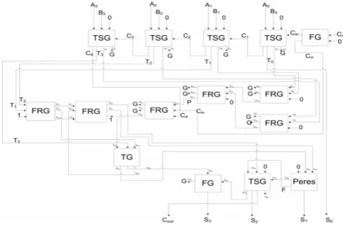
It uses two four bit adders, carry skip logic circuits and a correction logic circuit . Carry skip logic may generate the carry out, Coutinstantaneously. We will present these components with proper algorithms and appropriate figures. The proposed design is found to be much better than the existing one [11] in terms of number of gates, number of garbage and delay. . The quantum cost of the 2*2 reversible logic gate is taken as unity. the result of the binary addition of the two BCD numbers overflow is checked by combinational circuit for BCD detection. Proper expression for this condition is: Pi = Ai⊕Bi and Cin to the block will propagate to the carry output of the block if the entire Pi’s are set. In this way, we can generate Coutwithout waiting for it to be generated in ripple carry fashion. Let, the propagation signal for the block is denoted by P. Then, P = P3.P2.P1.P0. If P is set, Cin will be propagated to the Cout. However, in the other case, Cout will be generated in the ripple carry fashion. So, carry skip logic bit of the block is K = P.Cin+ C4 where C4 is the carry generated in the ripple carry fashion. The overall overflow detection bit, F= (T1+T2). T3⊕ K is generated in the same way with Reversible BCD adder presented earlier in this paper. Overflow correction logic incorporated is the same as the Reversible BCD adder.The following procedure (Algorithm 4.3.1) is used for the design of Carry Skip 1-digit BCD adder. This procedure is presented along with appropriate figure.
Algorithm CARRY_SKIP_BCD_ADDER_
ALGORITHM (
A, B, C
i)
Input:A (A3, A2, A1, A0)andB (B3, B2, B1,
B0) are two input vectors and Cin is the carry in.
Output: A BCD adder capable of performing the sum = A + B. The buffer vector S (Cout, S3, S2, S1,S0) will store the result.
begin
Step 1:ComputeP (propagate bit). Initially P:=truefor all i in {0, 1… 3} do P: = P AND (Ai⊕ Bi).
Step 2: Compute T: = {C4, T3, T2,T1,T0}, where
Ti: = Ai⊕ Bi ⊕ Ci and Ci’s are generated from each adder block. Step 3: Compute carry skip logic bit, K:=P.Cin + C4.
Step 4: The overall overflow detection bit F: =
(T1+T2)T3 ⊕ K, which is true whenever a BCD overflow is detected. Step 5: Add binary 0110 to T if overflow detection bit F istrue.
Step 6: Compute S: = (Cout, S3, S2, S1,S0), the final sum of the addition process. ReturnS;
end
1763 | P a g e
The Fredkin gates in the middle of the Figure 4.3.1 generate the block propagation, P and carry skip logic bit, K.Fredkin gates and Toffoli gate on the left side performs the BCD overflow detection same as for reversible BCD adder. BCD overflow correction logic is also like the reversible BCD adder. Table 2 shows the comparative analysis of the improved Carry Skip Reversible BCD adder with the one presented in [11] and it clearly shows that the proposed design outperforms the existing one in every metrics. Circuit presented in [11] allows multiple fan-outs that are prohibited in strict reversible sense.Output waveform of BCD adder
Output waveform of carry skip 1digit BCD adder
IV. CONCLUSIONS
1764 | P a g e
has the potential to perform the desired operation much faster. BCD adders can be an important part of some other larger and more complex reversible circuits. Fast and improved BCD adders may also find its use in future quantum computers [4].REFERENCES
[1] Keyes R, Landauer R. Minimal Energy Dissipation in Logic. IBM Journal of Research and Development 1970; 14: 153-7.
[2] Landauer R. Irreversibility and heat generation in the computational process’s. IBM Journal of Research Development 1961; 5: 183-91.
[3] Bennett CH. Logical reversibility of computation. IBM Journal of Research and Development 1973; 17: 525-32.
[4] Shende VV, Prasad AK, Markov IL, Hayes JP. Synthesis of reversible logic circuits. IEEE Transaction on CAD 2003; 22.(6): 723-9.
[5] Moore GE. Cramming more components onto integrated circuits. Journal of Electronics 1965; 38(8). [6] Frank M. Physical Limits of Computing. CIS 4930.1194X/6930.1078X, 2000.
[7] Perkowski M. Reversible Computation for Beginners. Lecture Series 2000. Portland State University. http://www.ee.pdx.edu/~mperkows.
[8] Hayes JP. Computer Architecture and Organization, 3rd ed. McGraw-Hill; 1998.
[9] Babu HMH, Chowdhury AR. Design of a Compact Reversible Binary Coded Decimal Adder Circuit. [10]Babu HMH, Islam MR, Chowdhury AR, Chowdhury SMA. Synthesis of full-adder circuit using reversible logic. 17th International Conference on VLSI Design 2004; 757-60.
[11]Thapliyal H, Kotiyal S, Srinivas MB. Novel BCD Adders and their Reversible Logic Implementation for IEEE 754r Format. 19th International Conference on VLSI Design 2006; 387-92.
[12]Khan M. H. A andPerkowski M. Multi-output ESOP synthesis with cascades of new reversible families. 6th International Symposium on Representations and Methodology of Future Computing Technologies, March 2003, 144-153.