Comprehensive RCS Simulation of Dispersive Media
Using SO-FDTD-DPW Method
Farid Mirhosseini* and Bruce Colpitts
Abstract—Perfectly Matched Layer (PML) is modeled by Split-Field FDTD (SF-FDTD) in order to simulate Radar Cross Section (RCS) of a plasma slab. PML is used as an absorbing boundary, and discrete plane wave (DPW) is employed to generate plane wave. DPW method has a power isolation of −300 dB between scattered-field and total-field regions. The dispersive media is modelled by shift-operator FDTD. In this article, the SO-FDTD and DPW are combined, and it is proved that this combination shows a good stability. Finally, two different plasma profiles (exponential and polynomial) are used to prove reflection coefficient of a conductive layer can be reduced by choosing true profile of covering layer. By using Near-to-Far-Field Transformation, all fields are transferred to far-field region to calculate RCS.
1. INTRODUCTION
One of the first problems in electromagnetic modelling is the formulation of absorbing boundaries to simulate infinite space and prevent reflections resulting from grid truncation. There are two popular absorbing boundary conditions (ABC) in use today, the Mur method [1, 2] and the perfectly matched layer (PML) method [3]. Until 1993 all absorbing boundary conditions including Mur were limited in their ability to treat grazing incident waves. In 1994, Berenger proposed split-field PML (SF-PML) for 2D, and in 1996 he developed a formulation to be employed for 3D space [4, 5]. The perfectly matched layer (PML) is generally considered the state-of-the-art for the termination of FDTD grids. There are some situations where specially designed ABC’s can outperform a PML, but this is very much an exception rather than the rule [6, 7]. The theory behind a PML is typically perfect in the continuous world, for all incident angles and for all frequencies. However, when a PML is implemented in the discretized world of FDTD, there are always some imperfections or reflections present.
Another challenging part in the modelling and simulation problems of electromagnetic waves is plane wave implementation. One of the most significant problems in electromagnetics is to predict the radar cross-section (RCS) of an object where it is assumed that the source is far away. For accurate calculation or prediction of RCS, one needs to have a good approximation of a plane wave. Plane waves have many other applications including telemetry or object-detection in multilayer structures. The first method proposed for numerical plane wave implementation was by Sadiku [8]. In 1995, Taflove proposed the total-field/scattered-field (TFSF) formulation outlined in [9]. This technique was perfectly developed for 1D, 2D and 3D space. In the finite-difference time-domain (FDTD) method, scattering problems are most often simulated by using the total-field/scattered-field (TFSF) formulation.
In order to implement TFSF, the computational domain is separated into two regions: the total field (TF) region where the scattering object, and both incident and scattered fields reside; and the scattered field (SF) region, where only the scattered fields, the output of interest, reside. There is a TFSF boundary which separates the grid into two regions, TF and SF. There were two nodes adjacent
Received 6 May 2015, Accepted 12 July 2015, Scheduled 28 July 2015
* Corresponding author: Farid Mirhosseini ([email protected]).
to this boundary. One is in the SF region and depended on a node in the TF region. The other is in the TF region and depends on a node in the SF region. To obtain self-consistent update equations, when updating nodes in the TF region, one must use the total field which pertains at the neighboring nodes. Conversely, when updating nodes in the SF region, one must use the scattered field which pertains at neighboring nodes.
An absorbing boundary condition simulates the open problem, and serves to cancel unwanted numerical reflections corrupting the scattered field. With the advent of PML, these reflections can be reduced to practically any desired level of accuracy. The TF/SF technique is based on a lookup table generated by interpolation between two adjacent cells on 1D auxiliary grid. Introducing the lookup table decreases the memory needed for computation and makes this method computationally efficient. The plane wave sources are introduced at the Huygen’s surface to account for discontinuity between TF and SF regions. The power leakage achieved by the TF/SF method is −40 dB for the best condition regarding the wave incident angle. One part of this error comes from interpolation error, and another part is a result of numerical dispersion mismatch between the 1D incident field array (IFA) and 3D wave propagation in TF region. To improve the IFA method, signal processing techniques [10] and optimizing the dispersion mismatch using matched numerical dispersion(MND) [11, 12] were proposed. Combining these two techniques reduces the power leakage caused by non-physical reflections on Huygen’s surface to −70 dB.
Another technique proposed to implement numerical plane wave is Analytic Field Propagator (AFP) [13, 14]. In this method, the plane wave function is constructed in the frequency domain directly from the dispersion relationship. In the Yee FDTD grid, it is possible to calculate the time series at an arbitrary point, given the incident field at a reference point and the direction of propagation. This allows one to realize an exact TFSF boundary for arbitrary directions of propagation. This method provides −180 dB of power isolation.
The method used for this paper is discrete plane wave (DPW) proposed by Tan and Potter in 2007 for 1-D space [15] and then developed for 3-D [16]. In contrast to IFA method, this method uses six 1-D auxiliary grids for each field and eliminates the need for interpolation. There is no dispersion mismatch, so it leads to a perfect plane wave implementation and TF/SFpower leakage for this method is less than−300 dB. A 12-layer Split-Field PML is used for the ABC. The dispersive media are modelled by shift-operator FDTD [17–19]. Near-to-Far-Field transformation (NTFT) is applied to calculate RCS in far-field [20]. This NTFT method is based on the surface equivalence theorem described by Balanis [21]. Finally, the Fast Fourier Transform (FFT) is used to transform time domain signals to the frequency domain.
2. FORMULATION
2.1. Split-Field PML
The split-field PML works by separating the electric and magnetic fields of the incident wave into two components on the ABC. The component’s plane of integration is tangential to the ABC surface, and the one normal to that. Only the latter needs to be attenuated by employing the ABC via the creation of artificial bi-anisotropic media that selectively apply the loss. These increase the number of Maxwell’s equations from six to twelve equations. By using some simplifications the number of equations can be reduced to ten equations as they are described in (1) to (10).
μ0∂Hxy
∂t = ∂Ez
∂y (1)
μ0∂Hxz
∂t +σmzHxz= ∂
∂z(Eyx+Eyz) (2) μ0∂Hyz
∂t +σmzHyz= ∂
∂z(Exy+Exz) (3) μ0∂Hyx
∂t = ∂Ez
∂x (4)
μ0∂Hz
∂t = ∂
∂x(Eyx+Eyz) + ∂
0∂Exy
∂t = ∂Hz
∂y (6)
0∂Exz
∂t +σzExz= ∂
∂z(Hyx+Hyz) (7) 0∂Eyz
∂t +σzEyz= ∂
∂z(Hxy +Hxz) (8) 0∂Eyx
∂t = ∂Hz ∂x (9) 0∂E ∂t = ∂
∂x(Hyx+Hyz) + ∂
∂y(Hxy +Hxz) (10)
These equations can be discretized to be suitable for simulations. As long as the impedance of the lossy material matches the impedance of the interior domain which is free space, the reflection from the ABC interface can be eliminated. This matching condition is shown in (11).
σ σm
=
μ (11)
where σ and σm are electric and magnetic conductivities. In order to have no reflection on the PML
interface, σ must be increased gradually from interface surface outward. The back of the PML is usually terminated by a PEC layer. In theory, σ and σm are continuous, but when field equations are
discretized, bothσandσm must be discretized. To optimize the value of these conductivities in different
layers, some research has been conducted [4, 22]. Within the PML, the conductivity was scaled using polynomial scaling [22].
σζ(ζ) = σζmax|ζ−ζ0| m
dm , ζ =x, y, z (12)
where ζ0 is the interface, d the depth of the PML, and m the order of the polynomial. A choice for
σζmax to minimize reflection is as [20]
σζmax =σopt ≈ m
+ 1
150πΔζ (13)
2.2. Discrete Plane Wave
The discrete plane wave method was proposed by Tan and Potter in 2010 [16] to overcome errors generated in the IFA method from interpolation and numerical dispersion mismatch. In contrast to IFA, this method employs six 1-D auxiliary grids where each grid is used to generate one of the electric or magnetic fields. In general, spacing for any grid can be non-uniform. It means Δrx= Δry= Δrz, but
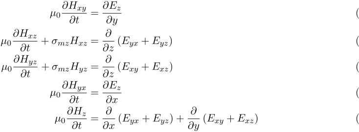
such non-uniformity makes the relation among all six components very difficult to evaluate. However, the spacing can be uniform, and the relation between six auxiliary grids can be evaluated for specific angles of incidence called rational angles. In this case, Δζ =pζΔζ =mζΔr, where mζ is an integer, and pζ is
any of three components of propagation vector direction,P = (px, py, pz) = (sinθcos∅,sinθsin∅,cosθ).
The anglesθand ∅are azimuthal and polar angles used for subspace projections. Using this definition, any point in the main 3D grid can be found by the following equation:
r≡irΔr =pxIΔx+pyJΔy+pzKΔz= [Imx+Jmy+Kmz] Δr (14)
where I, J and K are the number of cells at the same direction of x, y and z. Figure 1 clarifies this concept for the yz plane, and it can be developed to yx and xz planes. The rational angles for which (14) comes true can be calculated as:
⎧ ⎪ ⎪ ⎪ ⎨ ⎪ ⎪ ⎪ ⎩
sin∅=myΔx
m2
xΔ2y+m2yΔ2x
tanθ=
p2
x+p2y
p2
z
pζ =
mζΔr
Δζ
Figure 1. Reconstruction of fields at any point of main grid based on auxiliary grid fields.
Since there are infinite combinations on mζ and Δζ, there will be an infinite number of incident
angles at which the plane wave can be generated in the main grid.
The electric and magnetic fields must be constructed using (16) and (17), which are discretized Maxwell’s equations.
Hζ
n+ 1
ir+mζ/2=Cha·Hζ
n
ir+mζ/2+Chb,ζ+1·
Eζ+2
n+ 1/2
ir+mζ−mζ+1/2−Eζ+2
n+ 1/2
ir+mζ+mζ+1/2
+Chb,ζ+2·
Eζ+1
n+ 1/2
ir+mζ+mζ+2/2 −Eζ+1
n+ 1/2
ir+mζ−mζ+1/2
(16)
Eζ
n+ 3/2
ir+mζ+1+mζ+2/2=Cea·Eζ
n+ 1/2
ir+mζ+1+mζ+2/2 +Ceb,ζ+1·
Hζ+2
n+ 1
ir+mζ+1+mζ+2/2
−Hζ+2
n+ 1/2
ir+mζ+mζ+1/2
+Ceb,ζ+2·
Hζ+1
n+ 1
ir+mζ+1/2
−Hζ+1
n+ 1
ir+mζ+1+mζ+2/2
(17)
whereζ =x,ζ+ 1 =y and ζ+ 2 =z.
Another significant aspect of the DPW method is source generation. In this method, hard sources have to be used instead of soft sources. If ψ is the polarization angle defined in [9], then E-field polarization projection can be defined as Pζ,ψ . For instance, Px,ψ = sinψsinφ+ cosψcosϑcosφ. If
fH(tn) is the source function applied to the grid at reference point X0 = 0(0,0,0), then for any spatial shift [mζ/2 +ir]Δr, a time delay [mζ/2 +ir]Δr√μ will occur. A plane wave in the 3-D grid can be
generated byE-field using (16) and (17) where the hard source is imposed based on:
Eζ
n+ 1
ir+mζ/2 =P
ζ,ψ·fE
tn+1−
m
ζ
2 +ir
Δr√μ
for 0≤ir≤max{|mζ|} (18)
Although one can generate plane wave using (16), (17) and (18), the shape of the plane wave generated by this method is not exactly the same as the initial hard source function. The reason for that is the numerical reflection on 1-D grids due to the truncation. In order to cope with this issue, we use Optimized Analytic Field Propagator (O-AFP) [13, 14]. In this method, the Fourier transform of the initial wave function must be calculated, and then since the wave numberk(ω) is frequency dependent the delay at any point of 1-D grid can be calculated for each frequency by introducing a phase factor as shown in (19).
Einc,ζ|rζ=Einc|rref ·Pζ,ψ ·e−jk(ω)(rζ−rref) (19)
whererref is the reference point on the 1-D grid where the hard source is applied. Having the spectrum
2.3. Shift-Operator FDTD
The technique used to simulate plasma as a dispersive media is SO-FDTD. This method is based on the Auxiliary Differential Equation (ADE) method in which permittivity of the dispersive medium is expanded as a rational fraction function:
r(ω) =
N
n=0pn(jω)
n
N
n=0qn(jω)
n (20)
Then by usingjω→∂/∂t, the frequency domain can be transformed to time-domain. In this way, the third differential equation can be made from the frequency domain equation:
D(t) =ε0εr
∂ ∂t
E(t) (21)
If central difference is used, (21) can be discretized. Assumingy(t) =∂f(t)/∂(t), one can write:
yn+1+yn
2 =
fn+1−fn
Δt (22)
In general,ztfn=fn+1, wherezt is shift operator. Equation (22) can be written as:
yn =
2 Δt
zt−1
zt+ 1
fn (23)
∂/∂t→
2 Δt
zt−1
zt+ 1
(24)
Substituting (24) and (20) in (21), the constitutive relationship for dispersive media in the time domain can be written as:
K
k=0qk
2 Δt
zt−1
zt+ 1
k
Dn=ε0
K
k=0pk
2 Δt
zt−1
zt+ 1
k
En (25)
Considering the un-magnetized plasma permittivity as:
εr = 1 +
ωpe2
jω(jω+v) (26)
whereωp andv are the plasma frequency and collision rate. We can identify the coefficients qk and pk;
sop2 = 1, p1 =v,p0 =ωpe2 and q2 = 1, q1 =v,q0 = 0. Having these coefficients, the update equation for electric fields resulted from (25) will be:
En+1= 1
ε0
ω2
peΔt2+ 2vΔt+ 4
(2vΔt+ 4)Dn+1−8Dn+ (−2vΔt+ 4)Dn−1−ε0
2ω2peΔt2−8En
−ε0
ωpe2 Δt2−2vΔt+ 4En−1 (27)
2.4. NTFT
In the FDTD method, the fields are calculated in the near-field, so they must be transformed to the far-field to be able to calculate RCS. This NTFT transformation is based on the equivalence surface theorem described in [19, 20]. Two radiation vectors N and L are calculated using two integral equations:
N=
S
JSexp
jkrrˆ
dS (28)
L=
S
MSexp
jkrrˆ
dS (29)
where harmonic scattered surface currents −J→S = ˆn×H, and −→MS = E ×nˆ exist on the surface, when
wavenumber, ˆrthe unit vector to the far zone field point,rthe vector to the source point of integration, andS the closed surface surrounding the scatterer. After findingN andL, the time harmonic far zone scattered electric fields are:
Eθ=−jexp(jkR) (ηNθ+L∅)/(2λR) (30)
E∅=−jexp(jkR) (−ηN∅+Lθ)/(2λR) (31)
where η is the impedance of free space and R the distance from origin to the far zone field point. By discretizing these two equations, they can be used for numerical simulations. However, for some specific conditions such as strongly forward scattering objects, the integral is not needed to be calculated on the whole surface [23].
3. SIMULATION RESULTS
Based on the theory explained in the previous section, simulation is done on dispersive media with permittivity specified in (26). For this simulation, a Gaussian derivative pulse is as shown in (32), and Figure 2 is used to make the plane wave.
Ez(t) =
10−5 −2 (t−3T)
T2
·exp ((−(t−3T)/T)2 (32)
Figure 2. The input wave function to generate plane wave.
Figure 3. AY Z cut plane in the middle of SF/TF region when scatterer is located in TF region.
(a)
(b)
Figure 4. Comparison between simulation result and analytic solution of a short dipole antenna at 0.5 m from antenna.
The simulation space is a 70×70×70-cell cubic region. Twelve layers from each side are used for SF-PML as the absorbing boundary, and the conductivity in this anisotropic region is chosen to have a reflection coefficient of 10−7 on the PML-free space interface. There are 3-cell layers between the PML and SF/TF interfaces. This region is the scattered field region from which the far fields are calculated. The TF region is a 40×40×40-cell cubic region, and the scatterer is located in this region as shown in Figure 3.
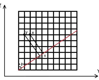
For plane wave we choose T = 0.1 ns, Δt = 5 ps and space step (Δ = 3 mm). In order to prove that the SF-PML layer works, a dipole antenna is located in the middle of the free space or simulation region, and then the response is compared with the analytical solution of the dipole antenna at 0.5 m from the dipole antenna. As shown in Figure 4, there is good agreement between simulation and analytic solutions. Figure 4(a) shows the signal in time-domain, and Figure 4(b) is the frequency response using FFT. To verify the simulator, a parallel polarized wave is applied when there is no object in the TF region, and then power leakage on TF/SF interface is calculated as shown in Figure 5. It shows 150 dB isolation between electric fields of TF/SF interface which is 300 dB in terms of power leakage.
To verify the fields in the TF region, a dielectric sphere is located in the TF region, and the normalized electric fields (Ey and Ez) are calculated by applying a sine wave for f0 = 2.5 GHz. These fields are compared with the Mie exact solution [24] for dielectric permittivity of (r = 4). Figure 6
(a) (b)
Figure 6. Normalized electric fields (Ez and Ex) on the axis of dielectric sphere. (a) EEy0. (b) EEz0.
Figure 7. Comparison between measured and simulated RCS of PEC at different wavelengths.
shows these fields on the axis of the dielectric sphere. The sphere radius is 15 cells (4.5 cm), and the center is at cell number 35.
In order to verify the RCS achieved by the designed code, a thin PEC sheet (d= 3 mm,a= 93 mm and b= 93 mm) was located in the TF region, and the RCS was compared to measured RCS for a few specific frequencies [25]. Figure 7 shows the calculated and measured RCS of this PEC sheet.
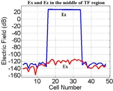
Figure 8 reveals the RCS of a plasma slab with a thickness of one cell for different ωp when
υ= 1 GHz. Figure 9 shows the RCS of the same plasma slab for various collision rates whenfp= 5 GHz.
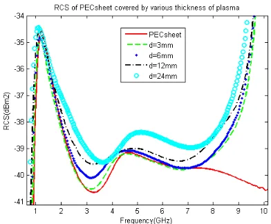
Both figures are in agreement with plasma physics predictions. Figure 10 compares the RCSs of a Perfect Electric Conductor (PEC) when it is not covered by a plasma layer and when it is covered by a plasma layer of different thickness. For this simulation the plasma frequency and collision rate are (fp= 5 GHz,
υ= 15 GHz).
Figure 11 shows the RCS of a PEC sheet covered by a 6 mm plasma layer for different incident angles. Since the object is symmetrical, the angles are changed from 0 to 90 degrees. The angle (φ) is in respect to the +x axis, so the maximum reflection occurs forφ= 90◦.
All previous simulations are done for the electric field in the +z direction or parallel to the sheet. Figure 12 shows the monostatic RCS of the same PEC sheet when the electric field is in the +xdirection, so the angle of electric field and the sheet changes by angle.
Figure 9. RCS of plasma slab of 3 mm thickness for various collision rate.
Figure 10. RCS of Perfect Electric Conductor (PEC) when it is not covered by plasma layer and when it is covered by plasma layer of different thickness.
Figure 11. RCS of PEC (a = 93 mm and b = 93 mm) covered by 6 mm plasma layer (E=Ez).
A PEC sheet is covered by two different plasma profiles, and the FDTD method is used to simulate reflection coefficient (R) from this layer. Equation (33) shows the complex refractive index for the film covering the conductive sheet. The equations for these two profiles are shown in Equations (34) and (35).
ˆ
nf(y) =nf(y) +jkf(y) (33)
nf(y) =nf0+ (nf d−nf0)
(df −y)
df
a
and kf(y) =kf0+(kf d−kf0)
(df−y)
df
a
(34)
nf(y) =Bn+Ane(a(df−y)/df) and kf(y) =Bk+Ake(a(df−y)/df) (35)
where An=
(nf d−nf0)
ea−1 ,Bn=−
(nf d−nf0ea)
ea−1 , Ak =
(kf d−kf0)
ea−1 and Bk =−
(kf d−kf0ea)
ea−1 . nf0 and kf0 are the real and imaginary parts of the refractive index of the film at film-free space interface. nf d and kf d
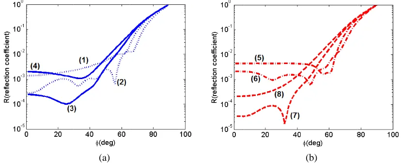
are the real and imaginary parts of the refractive index of the film at film-substrate interface, andais the order of polynomial or exponential function. Figures 13(a) and (b) show reflection coefficient for different orders (a). Figures 14(a) and (b) show reflection coefficient for different film thicknesses (df),
and Figures 15(a) and (b) show reflection coefficients for different incident angles (φ). It can be seen from these results that by choosing correct order of functions the minimum reflection is achieved. If the thickness of plasma layer increases, the order of functions must increase to have minimum reflections. Figures 13(a)-(5) show reflection coefficient when the conductive sheet is covered by homogeneous and real permittivity dielectric. It can be seen that for different orders the reflection coefficient remains very close to one, but when the imaginary part is added to refractive index the reflection decreases (Figure 13(a)-(6)). For Figure 14, simulations are done for three different orders (a= 3, 5 and 7), and it can be seen that for both TE and TM cases, the reflection decreases by increasing the thickness. Comparing Figures 13, 14 and 15, it can be revealed that reflection coefficient is more sensitive to the order of function or the gradient of refractive index than the thickness of plasma layer or the angle of incidence.
(a) (b)
Figure 13. Reflection coefficient from conductive sheet covered by inhomogeneous plasma profile, (a) TE mode (solid) polynomial and (dotted) exponential. For graphs (1, 2 and 3) kf d = nf d = 1,
kf0 = 0, nf0 = 1, (1) df = 0.06 m, (2) df = 0.09 m, (3) df = 0.21 m, (4) kf d = nf d = 105, kf0 = 0,
nf0 = 1, df = 0.21 m, (5) kf d = 0, nf d = 5, kf0 = 0, nf0 = 1, df = 0.21 m, (6) kf d = 10, nf d = 5,
kf0 = 1,nf0= 0,df = 0.06 m, (7)kf d =nf d= 105,kf0 = 0,nf0= 1,df = 0.21 m, (b) TM mode
(dash-dash) polynomial and (dash-point) exponential (8 and 9)kf d =nf d= 105,kf0 = 0,nf0= 1,df = 0.09 m
and 0.21 m respectively, (10)kf d=nf d= 1,kf0 = 0,nf0 = 1,df = 0.06 m, (11 and 12)kf d=nf d= 105,
(a) (b)
Figure 14. Reflection coefficient from conductive sheet covered by inhomogeneous profile (a) TE mode (solid) polynomial and (dotted) exponential. For graphs (1 and 2) kf d = nf d = 1, kf0 = 0, nf0 = 1, (1) a = 3.5, (2) a = 5, (3) kf d = nf d = 105, kf0 = 0, nf0 = 1, a = 5, (4) kf d = nf d = 1, kf0 = 0,
nf0 = 1,a= 5, (5) kf d =nf d= 105,kf0 = 1, nf0 = 0,a= 17, (b) TM mode (dash-dash) polynomial and (dash-point) exponential, (6) kf d=nf d = 1,kf0 = 0,nf0 = 1,a= 3.5, (7)kf d=nf d = 1,kf0= 0,
nf0 = 1, a= 5, (8) kf d =nf d = 105, kf0 = 0, nf0 = 1, a= 5, (9) kf d = nf d = 1, kf0 = 0, nf0 = 1,
a= 5, (10) kf d=nf d= 1, kf0= 0, nf0 = 1,a= 17.
(a) (b)
Figure 15. Reflection coefficient from conductive sheet covered by inhomogeneous profile (a) TE mode (solid) polynomial and (dotted) exponential and (b) TM mode (dash-dash) polynomial and (dash-point) exponential. For all graphskf d=nf d= 1,kf0 = 0, nf0 = 1,df = 0.09 m, (1, 3, 5 and 7)a= 3.5 (2, 4,
6 and 8)a= 5.
4. DISCISSION
electrons in the plasma layer. This code is written in MATLAB and runs on a PC Intel i5, taking 9 hours for a single case. SF-FDTD PML is a straight forward method to implement such simulations and enables us to control reflection on the PML-free space interface. DPW is a good choice since this method decreases TF/SF power leakage to 300 dB, and makes it suitable for small object RCS simulations. SO-FDTD method is proved to be a stable and reliable method to model dispersive media.
5. CONCLUSION
Based on the simulation results, it can be seen that by adding the plasma slab, reduction in RCS happens for a specific range of spectrum. Note that this reduction caused by absorption in plasma layer is very low, and if the thickness of plasma layer increases compared to the dimension of PEC, it causes an increase in RCS. For the Layer with thickness of 3 mm, this reduction is about 0.2 dBm2. Figures 11 and 12 reveal that by changing the polarization of electric field, the reflection or RCS will be changed. The result of simulation by different profiles shows that the reflected power from a conductive layer can be reduced if some specific profile is used. It is shown that the reflection cannot be changed just by using a material with real permittivity or homogeneous refractive index, but it decreases to a large extent by choosing in-homogeneous plasma for which imaginary part of permittivity is not equal to zero.
REFERENCES
1. Engquist, B. and A. Majda, “Absorbing boundary conditions for the numerical simulation of waves,”
Mathematics of Computation, Vol. 31, No. 139, 629–651, Jul. 1977.
2. Mur, G., “Absorbing boundary conditions for the finite-difference approximation of the time-domain electromagnetic field equations,” IEEE Transactions on Electromagnetic Compatibility, Vol. 23, No. 4, 377–382, Nov. 1981.
3. Berenger, J. P., “A perfectly matched layer for absorption of electromagnetic waves,” Journal of Computational Physics, Vol. 114, 185–200, 1994.
4. Berenger, J. P., “Perfectly matched layer for the FDTD solution of wave-structure interaction problems,” IEEE Transactions on Antennas and Propagation, Vol. 44, No. 1, 110–117, Jan. 1996. 5. Berenger, J. P., “Three-dimentinal perfectly matched layer for absorption of electromagnetic
waves,” Journal of Computational Physics, Vol. 127, 363–379, 1996.
6. Lu, M., M. Lv, A. A. Ergin, B. Shanker, and E. Michielssen, “Multilevel plane wave time domain-based global boundary kernels for two-dimensional finite difference time domain simulations,”Radio Science, Vol. 39, No. 4, Aug. 2004.
7. Kivi, J. and M. Okoniewski, “Switched boundary condition (XBC) in FDTD,” IEEE Microwave and Wireless Components Letters, Vol. 15, No. 4, 274–276, Apr. 2004.
8. Sadiku, M. N. O., “Finite difference method,” Numerical Techniques in Electromagnetics, 1st Edition, CRC Press, Boca Raton, Florida, 1992.
9. Taflove, A., Computational Electrodynamics — The Finite-difference Time-domain Method, 3rd Edition, Artech House, 2005.
10. Oguz, U. and L. Gurel, “An efficient and accurate technique for the incident-wave excitations in the FDTD method,”IEEE Trans. Microw. Theory Tech., Vol. 46, No. 6, 869–882, Jun. 1998. 11. Guiffaut, C. and K. Mahdjoubi, “A perfect wideband plane wave injector for FDTD method,”
Proc. IEEE APS. Int. Symp., Vol. 1, 236–239, Salt Lake City, UT, 2000.
12. Moss, C. D., F. L. Teixeira, and J. A. Kong, “Analysis and compensation of numerical dispersion in the FDTD method for layered, anisotropic media,” IEEE Transactions on Antennas and Propagation, Vol. 50, No. 9, 1174–1184, Sep. 2002.
14. Tan, T. and M. Potter, “Optimized analytic field propagator (O-AFP) for plane wave injection in FDTD simulations,” IEEE Transactions on Antennas and Propagation, Vol. 58, No. 3, 824–831, Mar. 2010.
15. Tan, T. and M. E. Potter, “1-D multipoint auxiliary source propagator for the total-field/scattered-field FDTD formulation,”IEEE Antennas and Wireless Propagation Letters, Vol. 6, 144–148, 2007. 16. Tan, T. and M. Potter, “FDTD discrete planewave (FDTD-DPW) formulation for a perfectly matched source in TFSF simulation,” IEEE Transactions on Antennas and Propagation, Vol. 58, No. 8, 2641–2648, Aug. 2010.
17. Yang, H. W., R. S. Chen, and Y. Zhang, “SO-FDTD method and its application to the calculation of electromagnetic wave reflection coefficients of plasma,” Acta. Phys. Sin., Vol. 55, No. 7, 3465– 3469, Jul. 2006.
18. Ge, D. B., Y. L. Wu, and X. Q. Zhu, “Shift operator method applied for dispersive medium in FDTD analysis,”J. Radio Sci., Vol. 18, No. 4, 359–362, Aug. 2003.
19. Yang, H. W., “A FDTD analysis on magnetized plasma of Epstein distribution and reflection calculation,”Comput. Phys. Commun., Vol. 180, 55–60, 2009.
20. Luebbers, R. J., K. S. Kunz, M. Schneider, and F. Hunsberger, “A finite-difference time-domain near zone to far zone transformation,”IEEE Transactions on Antennas and Propagation, Vol. 39, No. 4, 429–433, Apr. 1991.
21. Balanis, C. A.,Advanced Engineering Electromagnetics, 1st Edition, Wiley, New York, 1989. 22. Liu, G. and S. D. Gedney, “Perfectly matched layer media for an unconditionally stable
three-dimensional ADI-FDTD method,” IEEE Microwave and Guided Wave Letters, Vol. 10, No. 7, 261–263, Jul. 2000.
23. Li, X., A. Taflove, and V. Backman, “Modified FDTD near-to-far-field transformation for improved backscattering calculation of strongly forward-scattering objects,” IEEE Antennas and Wireless Propagation Letters, Vol. 4, 35–38, 2005.
24. Stratton, J. A., Electromagnetic Theory, 1st Edition, McGraw Hill Book Company, New York, 1941.