SYSTEM BASED ON GSM TECHNOLOGY
MWANGI PETER NGUGI
I56/24955/2013
A thesis submitted in partial fulfillment of the requirements for the award of the Degree of Master of Science (Electronics & Instrumentation) in the School of Pure
and Applied Sciences of Kenyatta University.
DECLARATION
This thesis is my original work and has not been presented for the award of a degree
or any other award in any University.
Mwangi Peter Ngugi
Signature ……… Date ………..
We confirm that the candidate carried out the work reported in this thesis under our supervision
Prof. Elijah Mwangi
School of Engineering
University of Nairobi/ Kenyatta University
Signature ……….. Date ………
Dr. Patrick Karimi
Institute of Energy and Research (IESR)
Kenya Power
DEDICATION
This work is dedicated to my loving wife, Purity, to my dear children, Precious and
ACKNOWLEDGEMENTS
It gives me great pleasure to express my sincere gratitude to my supervisors Prof.
Elijah Mwangi and Dr. Patrick Karimi for their invaluable guidance, motivation, constant inspiration and above all their ever co-operating attitude that enabled me
come up with this thesis in the present form. My sincere thanks are also extended to
all lecturers and laboratory technical staff in the Physics department for their support.
The most important part of my life is my family. Thanks to my lovely children
Precious and Peniel who are a source of inspiration in the pursuit of my dreams. I would never have been able to accomplish any of my goals without the support my
lovely wife Purity. I wish to thank her for love, encouragement and sacrifice throughout my study. Most importantly, I also wish to thank the almighty God for everything, for I believe that his great blessing has enabled me to make progression in
TABLE OF CONTENTS
DECLARATION ... ii
DEDICATION ... iii
ACKNOWLEDGEMENTS ... iv
LIST OF FIGURES ... ix
LIST OF TABLES ... x
ABBREVIATIONS AND ACRONYMS ... xii
ABSTRACT ... xiv
CHAPTER ONE ... 1
INTRODUCTION ... 1
1.1 Background to the study ... 1
1.1.1 Displacement water meters ... 2
1.1.2 Velocity water meter ... 3
1.2 Meter Reading ... 4
1.3 Statement of the research problem ... 5
1.4 Objectives ... 6
1.4.1 General objective... 6
1.4.2 Specific objectives ... 6
1.5 Rationale for the research ... 6
1.6 Scope of the study ... 7
1.7 Thesis Outline... 7
1.8 Note on publication ... 8
CHAPTER TWO ... 9
LITERATURE REVIEW ... 9
2.1 Introduction ... 9
2.2 Automatic meter reading ... 9
2.3 Related works ... 9
2.4 Proposed investigation ... 12
CHAPTER THREE ... 13
THE PIC18F4550 MICROCONTROLLER... 13
3.1 Introduction ... 13
3.2.1 PIC18F4550 Architecture ... 14
3.2.2Data Memory ... 15
3.2.3 Programme Memory ... 16
3.2.4 Programme stack memory ... 18
3.3 Registers ... 19
3.3.1 EECON1 AND EECON2 Registers ... 19
3.3.2 Table Latch (TABLAT) Register ... 20
3.3.3 Table Pointer (TBLPTR) Register ... 20
3.4 I/O PORTS ... 21
3.4.1 PORTA ... 22
3.4.2 PORTB... 22
3.4.3 PORTC... 23
3.4.4 PORTD ... 23
3.4.5 PORTE ... 24
3.5 Interrupts ... 24
3.6 Timer module ... 26
3.6.1 Timer0 module ... 26
3.6.2 Timer1 module ... 28
3.6.3 Timer2 module ... 30
3.6.4 Timer3 Module ... 31
3.6.5 Watchdog Timer ... 33
3.7 Oscillators ... 33
3.7.1 Oscillator control ... 34
3.7.2 Oscillator types ... 34
3.8EUSART ... 35
3.8.1 Registers in the EUSART ... 35
3.8.2 EUSART asynchronous mode... 37
3.8.3 EUSART synchronous master mode ... 37
3.8.4 EUSART Synchronous Slave Mode ... 37
CHAPTER FOUR ... 38
TECHNICAL CHOICE OF THE SYSTEM SOFTWARE AND HARDWARE ... 38
4.1 Introduction ... 38
4.2 Mikroc Integrated Development Environment ... 38
4.4 Power supply ... 40
4.4.1 Transformer ... 41
4.4.2 Rectification ... 42
4.4.3 Capacitor filter ... 42
4.4.4 Regulation ... 43
4.5 Liquid Crystal Displays (LCDs) ... 43
4.6 Global System for Mobile Communications (GSM) ... 46
4.6.1 GSM Network Architecture ... 46
4.6.2 Mobile Station (MS) ... 47
4.6.2.1 Mobile Equipment (ME) ... 47
4.6.2.2 Base Transceiver Station (BTS) ... 47
4.6.3 Base Station Controller (BSC) ... 48
4.6.4 Mobile Switching Center (MSC) ... 48
4.7 Flow sensors and measurements ... 49
4.7.1Flow measurement ... 49
4.7.2 Turbine Flow meter ... 50
4.7.3 Flow sensor ... 49
4.8 Solenoid valve ... 51
CHAPTER FIVE ... 53
RESEARCH METHODOLOGY ... 53
5.1 Introduction ... 53
5.2 Hardware components ... 53
5.2.1 Flow sensor ... 54
5.2.2 Liquid Crystal Display to PIC 18F4550 microcontroller interface... 55
5.2.3 GSM interface to PIC18F4550 microcontroller ... 57
5.2.4 Solenoid control valve ... 58
5.3 Software design ... 60
5.3.1 Flowchart for the system software ... 60
5.3.2 Programme code development ... 62
CHAPTER SIX ... 66
RESULTS AND DISCUSSIONS ... 66
6.1 Introduction ... 66
6.3 System response to water flow at different frequencies ... 67
6.4 Flow rate calculation. ... 67
6.5 The GSM Module ... 70
6.6 Control valve ... 71
6.7 Regulated power supply ... 72
6.8 Testing the entire system and comparing to other systems ... 73
CHAPTER SEVEN ... 75
CONCLUSION AND RECOMMENDATIONS ... 75
7.1 Conclusion ... 75
7.2 Recommendations for future work. ... 75
REFERENCES ... 77
APPENDICES ... 80
Appendix A: Architecture of PIC18F4550 ... 80
Appendix B: Materials employed in the research ... 81
Appendix C :Schematics of the water meter system ... 82
Appendix D: Data sheet ... 83
Appendix E: Published paper ... 84
LIST OF FIGURES
.
Figure 1.1: PIC18F4550 pin diagram configuration ………...2
Figure 1.2: PIC18F4550 with harvard architecture…..……….….…..……...4
Figure 3.1: PIC18F4550 pin diagram configuration ………...14
Figure 3.2: PIC18F4550 with harvard architecture…...……….….…..……...14
Figure 3.3: Internal architecture of the microcontroller………...15
Figure 3.4: PIC18F4550 Data Memory Map………...16
Figure 3.5: Program memory map………...17
Figure 3.6: Table read operation………...20
Figure 3.7: Table write operation……….…....21
Figure 4.1: A picture of the PICkit™2 Starter Kit…...39
Figure 4.2: A schematic showing the block diagram of a regulated power supply….41 Figure 4.3: Smoothed varying direct current……….………..42
Figure 4.4: Schematic diagram of an LCD………..45
Figure 4.5: GSM architecture………..48
Figure 4.6: Internal structure of G1/2 flow sensor………...………..…...51
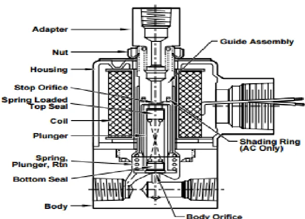
Figure 4.7: A solenoid valve………....51
Figure 5.1: Block diagram of the proposed intelligent water meter system………....53
Figure 5.2: Pin configuration of the G1/2 flow sensor………..54
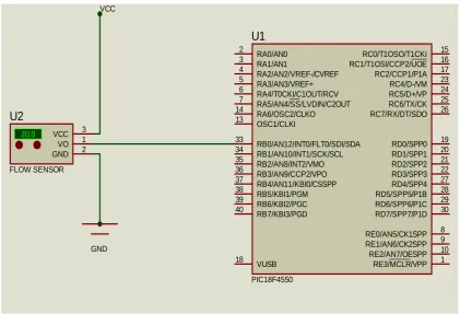
Figure 5.3: Flow sensor interface to PIC18F455……….55
Figure 5.5: GSM interface to PIC18F4550 microcontroller………..…………..58
Figure 5.6: Interface of Solenoid valve to the PIC18F4550………....59
Figure 5.7: Flowchart for the system software design……….61
Figure 5.8: A screenshot of Mikroc software illustating creation of new project…..62
Figure 5:9:A Screenshot illustrating selection of project name and project folder…..63
Figure 5:10: A Screenshot illustrating the process of addition or removal of files…..63
Figure 5:11: A Mikroc screen shot illustrating library selection………..64
Figure 5:12: A screenshot showing successful creation of a new project…...……...64
Figure 6.1: A picture of the proposed designed system………...66
Figure 6.2(a): Pulses at lower frequency…...………...67
Figure 6.2(b): Pulses higher frequency………...67
Figure 6.3: A picture of the valve used to control flow rate………...68
Figure 6.4: A graph of Frequency against Flow rate………69
Figure 6.5: A picture of a cell phone showing SMS received...71
LIST OF TABLES
Table 3.1: Registers associated with program memory………..19
Table 3.2: Ports of PIC 18F4550………..21
Table 3.3: Timer0 Control Register (T0CON)……….27
Table 3.4: Timer1 Control Register (T1CON)……….28
Table 3.5: Timer2 Control Register (T2CON)……….30
Table 3.6: Timer3 Control Register (T3CON)……….31
Table 3.7: Transmit status and control register………36
Table 3.8: Receive status and control register………..36
Table 3.9: Baud rate control register………....36
Table 4.1: The PIC kit™ 2 programmer pin functions………40
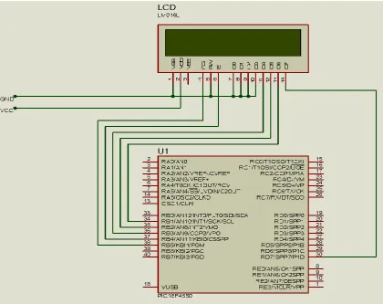
Table 5.1: Liquid Crystal Display pins configuration………..56
Table 6.1: Time(s) taken to fill 1 L at different frequencies………....68
Table 6.2: Flow rate at different frequencies………...69
Table 6.3: LCD and GSM readings………..70
Table 6.4: Table showing the response of the control valve to SMS………...71
Table 6.5: Output Voltage against loading of power supply ………...72
Table 6.6: Measured volume of the proposed design versus the actual volume……..73
ABBREVIATIONS AND ACRONYMS
ADC Analogue to Digital Converter
CPU Central Processing Unit
DAC Digital to Analogue Converter
EEPROM Electrically Erasable Read Only Memory
EUSART Enhanced Universal Synchronous Asynchronous Receiver
Transmitter
ETSI European Telecommunications Standards Institute
FOSC Frequency of the Oscillator
GPRS General Packet Radio Service
GPR General Purpose Register
GSM Global System for Mobile Communications
IDE Integrated Development Environment
I/O Input/output
LCD Liquid Crystal Display
MCU Microcontroller Unit
MMS Multimedia Messaging Service
Ofwat Office of water services (England and Wales)
PIC Peripheral Interface Controller
PLL Phase Locked Loop
RAM Random Access Memory
ROM Read Only Memory
SFR Special Function Register
UART Universal Asynchronous Receiver Transmitter
USART Universal Synchronous Asynchronous Receiver Transmitter
WAP Wireless Application Protocol
WDT Watchdog Timer
ABSTRACT
In the water distribution industry, meter reading is an important activity as source of revenue to the water utility company and at the same time it is meant to ensure accurate recording of consumption. Manual water meter reading is still being done in many countries in the world where employees of water companies take the readings from residential and business premises. Water bills are then prepared based on this data. This process is inefficient and costly in terms of man-hours, especially with the increase in residential houses in most of urban areas. The employees of water companies also face some difficulties in accessing some premises especially in the slum areas and hence the meter readings in such areas are estimated. The process of manual meter reading is both cumbersome and inaccurate. Different researchers have used different technologies in order to automate meter reading but very little has been done using the GSM technology. In addition to this, the earlier designs were expensive. In this research a prototype of an automatic water meter reading system
has been designed, fabricated and tested. It consists of G1/2 flow sensor, PIC18F4550
microcontroller and its interfacing board, SIM 900 GSM module, solenoid control valve. G1/2 flow sensor has been used for water flow detection, the solenoid control
CHAPTER ONE
INTRODUCTION
1.1 Background to the study
In many parts of the world analogue water meters have been installed by water companies to measure the consumer‟s water consumption. Water meters are read on a
monthly basis by authorized water meter reader hired by the water companies. The consumer‟s bill is computed based on the approved water rates and according to the
amount of water consumed. If the meter reading is not possible for instance where
there is no physical access to the meter, then the bill is prepared based on average consumption. This method is expensive and is also error prone. This traditional way of collecting information has shown noticeable disadvantages to the water companies
and to their clients due to discrepancies in the information collected manually.
Water meters generally fall into three categories: simple mechanical water meters, mechanical water meters with an electronic communication device, and fully
electronic water meters. Mechanical water meters are used to measure the volume of water used by residential and commercial buildings that are supplied by a public
water supply system. In most parts of the world, water meters measure flow in m3 over a period of time. However, for some considerable time, there has been a constant debate, as to the validity and accuracy characteristics of mechanical meters (Ofwat,
2013). This has led to the search for fully electronic meters. There are two main types of water meters for volumetric measurement; these are the displacement and velocity
1.1.1 Displacement water meters
This type of water meter is most often used in residential and small commercial
applications. Displacement meters are commonly referred to as positive displacement meters. The two common types are oscillating piston meters and mutating disk
meters. Either method relies on the water to physically displace the moving measuring element in direct proportion to the amount of water that passes through the meter. The piston or disk moves a magnet that drives the register. Positive displacement meters
are generally very accurate at the low-to-moderate flow rates typical of residential and small commercial users. Because displacement meters require that all water flows
through the meter to "push" the measuring element, they are generally not practical in large commercial applications requiring high flow rates or low pressure loss. Positive displacement meters normally have a built-in strainer to protect the measuring
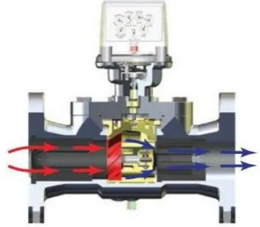
element from rocks or other debris that could stop or break the measuring element (Ofwat, 2013). The positive displacement meter is shown in figure 1.1
1.1.2 Velocity water meter
A velocity-type meter measures the velocity of flow through a meter of a known
internal capacity. The speed of the flow can then be converted into volume of flow to determine the consumption. The velocity- based meters include jet meters (single-jet
and multi-jet), turbine meters and electromagnetic flow meters. Most of these meters have an adjustment vane for calibrating the meter to the required accuracy. Multi-jet meters use multiple ports surrounding an internal chamber to create multiple jets of
water against an impeller, whose rotation speed depends on the velocity of water flow. Multi-jets are very accurate at low flow rates.
Turbine meters use the mechanical energy of the fluid to rotate the rotor in the flow stream. The speed of water flow is proportional to the rotor speed. Blade movement is detected magnetically. These meters are less accurate than displacement and jet
meters at low flow rates, but the measuring element does not occupy or severely restrict the entire path of flow. The flow direction is generally straight through the
meter, allowing for higher flow rates and less pressure loss than displacement-type meters. They are the meter of choice for large commercial users, fire protection and as
master meters for the water distribution system. They are accurate in normal working conditions but are greatly affected by the flow profile and fluid conditions (Mulley, 2004).
Electromagnetic flow meter is a velocity-type water meter, except that they use electromagnetic properties to determine the water flow velocity, rather than the
mechanical means used by jet and turbine meters. Electromagnetic flow meters apply Faraday‟s law of induction. They need alternating current or direct current electricity
from a power line or battery to generate the magnetic field. Since these flow meters
able to measure flow in both directions, and use electronic circuit for measuring and quantifying the flow. Magnetic flow meters can also be useful for measuring raw
water and waste-water, since there is no mechanical measuring element to get clogged or damaged by debris flowing through the meter. Since stray electrical energy flowing
through the flow tube can cause inaccurate readings, most of these meters are installed with either grounding rings or grounding electrodes to divert stray electricity away
from the electrodes used to measure the flow inside the flow tube (Mulley, 2004). A
velocity type meter is shown in figure 1.2.
Figure 1.2: Velocity type meter (Copyright IMAC Systems, Inc., Tully town, PA)
1.2 Meter Reading
In water meters the cumulative record of the number of units consumed are stored in a
register. The meters can be manufactured to read cubic meters. There are several ways in which meter reading can be accomplished.
a) Direct reading
b) Remote reading
This is where reading is done through an electronic signal, usually with a wire to a
separate station where the individual could either direct read or touch read.
c) Touch read or plug-in reader
This is where a handheld device is used. The device picks the electronic signal from plugging-in or touching the remote station and translates it into the number of cubic meters used. The remote station can even be on top of the meter pit lid. The readings
are stored on the hand-held device until the meter reader gets back to the office to be downloaded to a computer.
d) Automatic meter reading
This is a newer development which enables the meter reader to drive down the street and obtain the readings from the meters usually through radio transmission.
1.3 Statement of the research problem
In many parts of the world the reading of water meters is a manual task. Such a
process is monotonous, error prone and expensive in manpower utilization. In addition, some consumers may not be physically accessible or live in a hostile social
environment that is difficult to pay regular visits hence making it difficult to take water meter readings. The available water meter systems in such countries are not provided with the means of automating meter reading. With the growth of mobile
1.4 Objectives
1.4.1 General objective
The general objective of this research work is to design a cost effective system that will automate data collection of water consumption to allow utility companies to
provide efficient services to consumers.
1.4.2 Specific objectives
The specific objectives of this research work are;
i. To design a sensor system to detect presence of water in a pipe and the flow
rate.
ii. To develop and implement a C language-based program for flow rate and
volumetric flow determination using a PIC18F4550 microcontroller and display the same on the LCD.
iii. To develop and implement a C language-based program to enhance
communication between the PICF4550 microcontroller and GSM module,
sending and receiving of short messages through the GSM Network.
iv. To develop and implement a C language-based program to enhance
communication amongst the PICF4550 microcontroller, solenoid control valve
and GSM module, opening and closing the valve when a command is issued.
1.5 Rationale for the research
Currently, manual meter reading is still widely used in water meter system, and has been noted to be inefficient and costly in terms of man-hours. With the growth in
Microcontrollers can be used and are designed for embedded applications, have peripherals integrated on the same chip, can interface directly to sensors. A
microcontroller can employ sensors to detect flow rate and display the same on an LCD. It can serve as an efficient water billing system if interfaced to a GSM Modem
that sends data to the utility office.
1.6 Scope of the study
This research concentrated on developing an automatic water meter reading system since manual water meter reading is still being widely used in many parts of the
world. The system is GSM based. The billing process has been excluded but the display of the volume of water consumed in a given duration is included.
1.7 Thesis Outline
In this section an outline of the thesis is given.
Chapter 1 introduces the thesis, gives the objectives, rationale and the scope of the study. In chapter 2 a brief highlight on some water meter system designs that have been developed in the effort of automating water meter reading is given.
Chapter 3 gives a detailed discussion of the PIC18F4550 microcontroller. The areas discussed include the microcontroller features, architecture, registers, ports, interrupts,
timer modules, oscillators and EUSART.
In chapter 4 an explanation of Mikroc Integrated Development (IDE), PICkit2
programmer, Liquid crystal display, GSM module, Control valve and flow measurement is given.
Chapter 5 gives a description of the steps taken in the design of a GSM based water
meter system.
In chapter 7 a conclusion and recommendations for future work are given.
1.8 Note on publication
The contribution made in the course of the investigations reported in this thesis has
resulted in the following publication: Peter Mwangi, Elijah Mwangi and Patrick Karimi, “A Low Cost Water Meter System based on the Global System for Mobile
Communications,” International Journal of Computer Applications, vol 142, no.12,
CHAPTER TWO
LITERATURE REVIEW
2.1 Introduction
This chapter gives a brief highlight on some of the water meter system designs that
have been developed in the effort of automating water meter reading.
2.2 Automatic meter reading
Automatic Meter Reading System (AMR) is the remote collection of consumption data from customers‟ utility like energy meters, water meters among others using
radio frequency, telephony, power-line or satellite communications technologies and
process the data to generate the bill (Moghavvemi and Wong, 2005). With automatic
meter reading researchers have developed pulse or encoder registers to produce electronic output for radio transmitters, reading storage devices, and data logging
devices. Pulse meters send a digital or analogue electronic pulse to a recording device. The encoder registers have an electronic means permitting an external device to interrogate the register to obtain the stored reading.
2.3 Related works
Nelson (2014) designed a non-contact arrow pointer sensor design to reduce power consumption of low-cost and high accuracy hybrid water meter. This system involved embedding an electrical circuit into the body of a conventional mechanical water
meter, to be compatible with the currently used arrow meter. An electrical circuit was mounted on Printed Circuit Board (PCB) and only one low-cost PIC16F877A was
waveform. The detected result is then binary encoded and transmitted to a server. The data is transmitted through GSM network.
Yogendra and Tadwalkar (2014) implemented a GSM based water meter as a step towards automation in billing system. A paddle wheel flow sensor JT121 was used to
measure the water flow accurately with the help of rotating paddles. The system was able to send water usage within fraction of seconds in the form of text message by using existing GSM network. It gave better results than any other metering systems
such as mechanical, ultrasonic, electro-magnetic systems. By using this system, water consumption can be observed in real time. Such a system can also incorporate the
control of water consumption.
Ria et al. (2013) designed and developed an automatic flow meter for irrigation
systems which supplies only the required amount of water to crops. This saves water as well as energy. They employed a G1/2 Hall Effect water flow sensor as a sensing
unit with a turbine rotor inside it whose speed of rotation changes with the different rate of flow of water. The Hall Effect sensor gives an output of the corresponding
pulse train for frequency input to the microcontroller. The whole system comprised of
an AT89S52 microcontroller, G1/2 Hall Effect water flow sensor, relay, optocoupler, a
water pump, 5V supply, LCD, keypad and some passive components.
Rainer et al. (2013) developed remote automatic water meter reading system using
global system for mobile communications. The study aimed at developing an automatic water meter reading system that would enhance the analogue water meter data collection by utilizing wireless technology using GSM module system for data
and the software design. The hardware involved the analogue meter, the GSM module, the differential pressure sensor, and a desktop or a laptop. While the software
was developed in order to receive and to store data transmitted from the GSM module into the database and output graphically. A T-test was used to conduct and to verify if
the readings from the design were comparable to the actual volume measured from the analogue meter.
Santhosh and Roy (2012) proposed an intelligent flow measurement technique using an ultrasonic flow meter with an optimized neural network. The objective of their
work was to extend the linearity range of measurement to 100% of the input range, to make the measurement system adaptive to variations in pipe diameter, liquid density, and liquid temperature, and to achieve the above two objectives by an optimal
Artificial Neural Network.
Han and Myaing (2011) developed microcontroller-based water flow control system. In this system, the sensing unit consisted of a photo interrupter and slotted disk that
produced pulse train for frequency input of the microcontroller. This signal is
converted into flow rate by software program in PIC. This flow rate is compared to
the set point value. The microcontroller can control the water valve by using a DC
motor to vary the water flow rate based on this comparison.
Lee et al. (2008) developed a wireless digital water meter with low power consumption for automatic meter reading in which they used magnetic hole sensors to determine the amount of water consumption. They used ZigBee wireless protocol to
2.4 Proposed investigation
In the reported works, little or no attention has been paid to aspect of using GSM network to update the utility company on the consumption of water automatically
after certain duration of time. The proposed system seeks to pay more attention on use of GSM network to update the water utility company on water consumption. The
CHAPTER THREE
THE PIC18F4550 MICROCONTROLLER
3.1 Introduction
The chapter gives a detailed discussion on the PIC18F4550 microcontroller. The areas
discussed include the microcontroller features, architecture, registers, ports, interrupts, timer modules, oscillators and EUSART.
3.2 The PIC18F4550 Microcontroller chip
The PIC18F4550 is one of the advanced 8-bit microcontrollers developed by
Microchip Technology Inc. It belongs to PIC18F family of microcontrollers and has the following features.
i. It has five I/O ports of different sizes.
ii. It has a facility for generating the clock internally by operating in internal oscillator mode and therefore there is no need of an external crystal.
iii. It is a Nano watt technology, which can decrease the power consumption
during the operation.
iv. It works with the operating frequency of up to 48 MHz.
v. It has a program memory addressing up to 2MB and data memory addressing
4kB.
vi. It has a fast 10-bit analogue to digital converter.
vii. It has four general timers and a watchdog timer.
Figure 3.1: PIC18F4550 pin diagram configuration (www.microchip.com).
3.2.1 PIC18F4550 Architecture
The PIC18F4550 microcontroller has a Harvard architecture which include; Microprocessor unit, Program memory for instructions, Data memory for data, I/O
ports and support devices like timers. The advantage of this architecture is that instructions and data can be fetched simultaneously since they use two separate buses.
The PIC18F4550 Harvard architecture is illustrated in figure 3.2.
Figure 3.2: PIC18F4550 Harvard architecture. PIC18F4550
MPU
Programme memory
Data memory
(Special function and general
purpose registers) 16-bit instruction
bus
8-bit data bus 21-bit programme
address
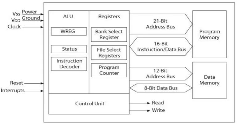
The internal architecture of PIC18F4550 microcontroller is illustrated in figure 3.3 while a detailed architecture of the microcontroller is given in appendix A.
Figure 3.3: Internal architecture of the microcontroller (www.microchip.com)
3.2.2 Data Memory
This memory is used for transitory data when the programme is being executed. It can
either be a SRAM or an EEPROM or both. An EEPROM is non-volatile whereas a
SRAM is volatile. The registers in the data memory have 12-bit address each which allow up to 4096 bytes of data memory. The data memory is divided into General
purpose Registers (GPR) and Special Function Registers (SFR).
The GPRs are used for data storage and scratchpad operations in the user‟s application while SFRs are used for control and status of the controller and peripheral functions. The instruction set and architecture allow operations across all banks. The
The bank selection is achieved by using bank select register (BSR). The PIC18F4550 microcontroller implements access bank to ensure SFRs and GPRs registers are
retrieved in a single cycle. The access bank is a 256-byte memory space that provides fast access to SFRs and the lower portion of GPR Bank 0 without using the bank
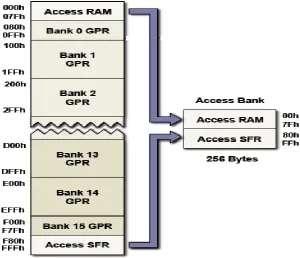
select register. Figure 3.4 illustrates the data memory map.
Figure 3.4: PIC 18F4550 Data Memory Map (www.microchip.com)
The memory map is divided into 16 banks each of 256B. The two access banks
termed as Access RAM and Access SFR are partitioned from bank 0 and bank 15. The Access RAM is at the top of the memory map with address 000h to 07Fh. The Access SFR is at the bottom of the memory map with address F80h to FFFh.
3.2.3 Programme Memory
The PIC18F4550 microcontroller has 32kB of flash memory and can store up to
16384 single word instructions. The memory is readable, writable and erasable during normal operation. A read from the program memory is executed on one byte at a time.
memory is erased in blocks of 64 bytes at a time. Instruction fetching stops during programme memory write or erase until the operation is complete. The programme
memory write or erase is terminated by an internal programming timer. A value written to program memory does not need to be a valid instruction. Figure 3.5 shows
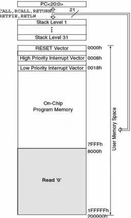
the program memory map
Figure 3.5: Program memory map (www.microchip.com)
The programme memory map comprises of programme counter, stack levels from 1 to
portion from address 8000h to 1FFFFFh. In order to read from or write into
programme memory, table read (TBLRD)and table Write (TBLWT) operations allow
the processor to move bytesbetween the program memory space and the data RAM.
The programme memory space is 16 bits wide, while the data RAM space is 8 bits wide. The tables read and write operations move data between these two memory spaces through an 8-bit register (TABLAT). The tables read operations retrieve data
from programme memory and place it into the data RAM space while table write operations store data from the data memory space into holding registers in programme
memory. The table operations work with byte entities. A table block containing data, rather than programme instructions, is not required to be word-aligned. Therefore, a table block can start and end at any byte address. If a table write is being used to write
executable code into programme memory, programme instructions will need to be
word-aligned. The programme memory can therefore access at most 2MB
instructions. Almost all instructions of PIC18 are 16-bit and therefore the instruction bus is 16-bit long. The program memory addresses are 21-bit address starting at
location 000000h.
3.2.4 Programme stack memory
The PIC18F4550 microcontroller contains a programme stack that stores up to 31
return addresses from functions. It is used to hold the return addresses for a subroutine call and interrupt processing. During a subroutine call the stack pointer is first incremented, the memory location it points to is written with the contents of the
program counter. During the return from the subroutine call, the memory location the stack pointer has pointed is decremented. When the return occurs within the function,
3.3 Registers
There are a number of control registers that are used in conjunction with the TBLRD and TBLWT instructions. They include:
a) EECON1 register
b) EECON2 register
c) TABLAT register
d) TBLPTR registers
The registers are illustrated in table 3.1.
Table 3.1: Registers associated with program memory (www.microchip.com)
3.3.1 EECON1 AND EECON2 Registers
The EECON1 register is the control register for memory accesses. The EECON2 register is not a physical register although it is used exclusively in the memory write and memory erases sequences. The MSB in the EECON1 register is term EEPGD and
is a control bit that determines if the access will be a program or data EEPROM memory access. When clear, any subsequent operations will operate on the data
EEPROM memory. When set, any subsequent operation will operate on the program
to the configuration/calibration registers or to program memory/data EEPROM memory.
3.3.2 Table Latch (TABLAT) Register
The Table Latch (TABLAT) is an 8-bit register mapped into the SFR space. The Table Latch register is used to hold 8-bit data during data transfers between the programme memory and the data RAM.
3.3.3 Table Pointer (TBLPTR) Register
The Table Pointer (TBLPTR) register addresses a byte within the programme
memory. It is comprised of three SFR registers which are Table Pointer Upper Byte (TBLPTRU) which is 6-bit wide, Table Pointer High Byte (TBLPTRH) which is 8-bit
wide and Table Pointer Low Byte (TBLPTRL) which is 8-bit wide. The three registers join to form a 22-bit wide pointer. The low-order 21 bits allow the device to address up to 2MB of program memory space. The 22nd bit allows access to the
device ID, the user ID and the Configuration bits. The Table Pointer, TBLPTR, is used by the TBLRD and TBLWT instructions. The table read operation with the
program memory and the data RAM is illustrated in figure 3.6
The table write operation with the program memory and the data RAM is illustrated in figure 3.7
Figure 3.7: Table write operation (www.microchip.com)
3.4 I/O PORTS
The PIC18F4550 microcontroller has five ports and each has three special function
registers for its operation. Table 3.2 shows the PORT description of the PIC18F4550
Table 3.2: Ports of PIC 18F4550 PORTS BUS SIZE BUS NAME
A 7 RA0-RA6
B 8 RB0-RB7
C 7 RC0-RC2 ,RC4-RC7
D 8 RD0-RD7
E 4 RE0-RE3
The ports have the following registers:
i) The TRIS register which provides direction functionality.
ii) The PORT register which reads logic levels on the input lines.
3.4.1 PORTA
PORTA is 7-bit wide and is a bidirectional port. Its corresponding data direction
register is TRISA. When TRISA bit is set, it makes the corresponding PORTA pin an input. When TRISA bit is cleared, it makes the corresponding PORTA pin an output.
The status of the pins is known by reading the PORTA while writing to it will write to the port latch. The Data Latch register (LATA) is memory mapped. Read-modify-write operations on the LATA register read and Read-modify-write the latched output value for
PORTA. The RA4 and RA6 pins are multiplexed with Timer 0 and the main oscillator respectively. All other PORTA pins have TTL input levels and full CMOS output
drivers. The TRISA register controls the direction of the RA pins, even when they are being used as analogue inputs. The bits in the TRISA register must be maintained set when using them as analogue inputs.
3.4.2 PORTB
This is an 8-bit wide port and is bidirectional. Its corresponding data direction register
is TRISB. When TRISB bit is set, the corresponding PORTB pin will be an input. Clearing a TRISB bit will make the corresponding PORTB pin an output. The data
latch register (LATB) is also memory mapped. Read-modify-write operation on the LATB register will read and write the latched output value for PORTB. Each of the PORTB pins has a weak internal pull-up. The RB7, RB6, RB5 and RB4 pins of
3.4.3 PORTC
PORTC is a 7-bit wide, bidirectional port. Its corresponding data direction register is
TRISC. When a TRISC bit is set, the corresponding PORTC pin will be an input. When a TRISC bit is cleared, the corresponding PORTC pin will be an output. The
RC3 pin is not implemented in the PIC18F4550. The Data Latch register (LATC) is also memory mapped. Read-modify-write operations on the LATC register will read and write the latched output value for PORTC. In addition the port is primarily
multiplexed with serial communication modules, including the EUSART, MSSP module and the USB module. Pins RC4 and RC5 are multiplexed with the USB
module. Both RC4 and RC5 have TTL input buffers instead of the Schmitt trigger buffers on the other pins. As digital ports, they can only function as digital inputs.
3.4.4 PORTD
PORTD is an 8-bit wide, bidirectional port. Its corresponding data direction register is TRISD. Setting a TRISD bit makes the corresponding PORTD pin an input while
clearing a TRISD bit makes the corresponding PORTD pin an output. The data latch register (LATD) is also memory mapped. Read-modify-write operations on the LATD
register will read and write the latched output value for PORTD. All pins on PORTD are implemented with Schmitt trigger input buffers. Each pin is individually configurable as an input or output. Each of the PORTD pins has a weak internal
pull-up. The weak pull-up is automatically turned off when the port pin is configured as a digital output or as one of the other multiplexed peripherals. The pull-ups are disabled
3.4.5 PORTE
PORTE is a 4-bit wide port. Its corresponding data direction register is TRISE. Three
pins RE0, RE1 and RE2 can be individually configured as inputs or outputs. These pins have Schmitt trigger input buffers. Setting a TRISE bit will make the
corresponding PORTE pin an input while clearing a TRISE bit will make the corresponding PORTE pin an output. When selected as an analogue input, these pins will read as „0‟s. In addition to port data, the PORTE register, TRISE controls the
direction of the RE pins, even when they are being used as analogue inputs. The pins must be maintained as inputs when using them as analogue inputs. The data latch
register (LATE) is also memory mapped. Read-modify-write operations on the LATE register will read and write the latched output value for PORTE.
The RE3 pin can only be configured as an input. Its operation is controlled by the MCLRE Configuration bit. When selected as a port pin, it functions as a digital input only pin; as such, it does not have TRIS or LAT bits associated with its operation. Otherwise, it functions as the device‟s Master Clear input. In either configuration,
RE3 also functions as the programming voltage input during programming.
3.5 Interrupts
An interrupt is an event that requires the processor to stop normal operation after
which a program code related to the event causing the interrupt is executed. They can be internally or externally generated. The PIC18F4550 has multiple interrupt sources and an interrupt priority feature that allows each interrupt source to be assigned a high
interrupt any low-priority interrupts that may be in progress. The high priority interrupt and low priority interrupts are illustrated in figure 3.5.
There are ten registers which are used to control interrupt operation. These registers are:
• RCON • INTCON
• INTCON2 • INTCON3
• PIR1 and PIR2 • PIE1 and PIE2 • IPR1 and IPR2
Each interrupt source has three bits to control its operation. The functions of these bits are:
(i). Flag bit to indicate that an interrupt event occurred.
(ii). Enable bit that allows program execution to branch to the interrupt vector
address when the flag bit is set.
(iii). Priority bit to select high priority or low priority.
The interrupt priority feature is enabled by setting the IPEN bit of the RCON register. When interrupt priority is enabled, there are two bits which enable
interrupts globally. When the interrupt flag enable bit and appropriate global interrupt enable bit are set, the address 0008h or 0018h will be selected, depending on the priority bit setting. Individual interrupts can be disabled through
For an interrupt to be accepted by the CPU the following conditions must be satisfied:
i) The global interrupt enable/disable bit GIE of INTCON must be set to 1.
ii) The interrupt enable bit of the interrupt source must be enabled. For instance,
if the interrupt source is external interrupt pin INT0, then the bit INT0IE of register INTCON must be set to 1.
iii) The interrupt flag of the interrupt source must be cleared. For instance, if the
interrupt source is external interrupt pin INT0, then the bit INT0IF of register INTCON must be cleared to 0.
iv) The peripheral interrupt enable/disable bit PEIE of INTCON must be set to 1
if the interrupt source is a peripheral.
3.6 Timer module
The PIC18F4550 has four general timers and a watchdog timer. The timers can
operate as counters and also in various modes.
3.6.1 Timer0 module
The Timer0 module incorporates the following features:
• Software selectable operation as a timer or counter in both 8-bit and 16-bit modes
• Readable and writable registers
• Dedicated 8-bit, software programmable prescaler • Selectable clock source (internal or external)
• Edge select for external clock • Interrupt on overflow
The T0CON register controls all aspects of the module‟s operation, including the
Table 3.3: Timer0 Control Register (T0CON)
R/W-1 R/W-1 R/W-1 R/W-1 R/W-1 R/W-1 R/W-1 R/W-1
TMR0ON T08BIT T0CS T0SE PSA T0PS2 T0PS1 T0PS0
Bit7 Bit 0
Bit 7 TMR0ON: Timer0 On/Off Control bit; 1 = Enables Timer0, 0 = Stops Timer0
Bit 6 T08BIT: Timer0 8-Bit/16-Bit Control bit; 1 = Timer0 is configured as an 8-bit
timer/counter, 0 = Timer0 is configured as a 16-bit timer/counter
Bit 5 T0CS: Timer0 Clock Source Select bit; 1 = Transition on T0CKI pin, 0 = Internal instruction cycle clock (CLKO).
Bit 4 T0SE: Timer0 Source Edge Select bit; 1 = Increment on high-to-low transition
on T0CKI pin, 0 = Increment on low-to-high transition on T0CKI pin
Bit 3 PSA: Timer0 Prescaler Assignment bit; 1 = Timer0 prescaler is NOT assigned,
Timer0 clock input bypasses prescaler, 0 = Timer0 prescaler is assigned. Timer0
clock input comes from prescaler output.
Bit 2-0 T0PS2:T0PS0: Timer0 Prescaler Select bits
111 = 1:256 Prescale value 110 = 1:128 Prescale value 101 = 1:64 Prescale value
100 = 1:32 Prescale value 011 = 1:16 Prescale value, 010 = 1:8 Prescale value
001 = 1:4 Prescale value 000 = 1:2 Prescale value
Timer0 operates either as a timer or a counter. The operation mode is selected by clearing the T0CS bit. In timer mode, the module increments on every clock by
default unless a different prescaler value is selected. If the TMR0 register is written into, the increment is inhibited for the following two instruction cycles. The user can work around this by writing an adjusted value to the TMR0 register. The Counter
mode is selected by setting the T0CS bit (= 1). In this mode Timer0 increments either on every rising or falling edge of pin RA4/T0CKI/C1OUT/RCV. The incrementing
3.6.2 Timer1 module
The Timer1 timer/counter module incorporates the following features: • Software selectable operation as a 16-bit timer or counter.
• Readable and writable 8-bit registers (TMR1H and TMR1L).
• Selectable clock source (internal or external) with device clock or Timer1 oscillator
internal options.
• Interrupt on overflow.
• Module Reset on CCP special event trigger.
• Device clock status flag (T1RUN).
The module incorporates its own low-power oscillator to provide an additional clocking option. The Timer1 oscillator can also be used as a low-power clock source for the microcontroller in power-managed operation.
Timer1 can also be used to provide Real-Time Clock (RTC) functionality to applications with only a minimal addition of external components and code overhead.
Timer1 is controlled through the T1CON Control register as shown in Table 3.4. It also contains the Timer1 Oscillator Enable bit (T1OSCEN). Timer1 can be enabled or
disabled by setting or clearing control bit, TMR1ON.
Table 3.4: Timer1 Control Register (T1CON)
R/W-0 R-0 R/W-0 R/W-0 R/W-0 R/W-0 R/W-0 R/W-0
RD16 T1RUN T1CKPS1 T1CKPS0 T1OSCEN T1SYNC TMR1CS TMR1ON
Bit 7 Bit 0
Bit 7 RD16: 16-Bit Read/Write Mode Enable bit
1 = Enables register read/write of Timer1 in one 16-bit operation
0 = Enables register read/write of Timer1 in two 8-bit operations
Bit 6 T1RUN: Timer1 System Clock Status bit
0 = Device clock is derived from another source
Bit 5-4 T1CKPS1:T1CKPS0: Timer1 Input Clock Prescale Select bits
11 = 1:8 Prescale value; 10 = 1:4 Prescale value; 01 = 1:2 Prescale value and 00 = 1:1 Prescale value
Bit 3 T1OSCEN: Timer1 Oscillator Enable bit
1 = Timer1 oscillator is enabled 0 = Timer1 oscillator is shut off
The oscillator inverter and feedback resistor are turned off to eliminate power drain.
Bit 2 T1SYNC: Timer1 External Clock Input Synchronization Select bit
When TMR1CS = 1:
1 = Do not synchronize external clock input 0 = Synchronize external clock input
When TMR1CS = 0:
This bit is ignored. Timer1 uses the internal clock when TMR1CS = 0.
Bit 1 TMR1CS: Timer1 Clock Source Select bit
1 = External clock from RC0/T1OSO/T13CKI pin (on the rising edge)
0 = Internal clock (FOSC/4)
Bit 0 TMR1ON: Timer1 On bit
1 = Enables Timer1
0 = Stops Timer1
The operating mode is determined by the clock select bit, TMR1CS. When TMR1CS
is cleared (= 0), Timer1 increments on every internal instruction cycle (FOSC/4). When the bit is set (= 1), Timer1 increments on every rising edge of the Timer1 external clock input or the Timer1 oscillator, if enabled. When Timer1 is enabled, the
3.6.3 Timer2 module
The Timer2 module timer incorporates the following features: •An 8-bit Timer and Period registers (TMR2 and PR2, respectively) • Readable and writable (both registers)
• Software programmable prescaler (1:1, 1:4 and 1:16) • Software programmable postscaler (1:1 through 1:16)
• Interrupt on TMR2 to PR2 match
• Optional use as the shift clock for the MSSP module
The module is controlled through the T2CON register as illustrated in table 3.5. The
register enables or disables the timer and configures the prescaler and postscaler. Timer2 can be shut off by clearing control bit, TMR2ON, to minimize power consumption.
Table 3.5: Timer2 Control Register (T2CON)
Bit 7 __ It is unimplementedRead as „0‟
Bit 6-3 T2OUTPS3 to T2OUTPS0: Timer2 Output Post scale Select bits
From 0000 to 1111 the postscale will be from 1:1 to 1:16 in the increasing order. Bit 2 TMR2ON: Timer2 on bit
1 = Timer2 is on 0 = Timer2 is off
Bit 1-0 T2CKPS1:T2CKPS0: Timer2 Clock Prescale Select bits
00 = Prescaler is 1 01 = Prescaler is 4 1x = Prescaler is 16
In the normal operation, TMR2 is incremented from 00h on each clock (FOSC/4). A 2-bit counter/prescaler on the clock input gives direct input, by-4 and
divide-by- 16 prescale options. These are selected by the prescaler control bits,
U-0 R/W-0 R/W-0 R/W-0 R/W-0 R/W-0 R/W-0 R/W-0
__ T2OUTPS3 T2OUTPS2 T2OUTPS1 T2OUTPS0 TMR2ON T2CKPS1 T2CKPS0
T2CKPS1:T2CKPS0. The value of TMR2 is compared to that of the Period register, PR2, on each clock cycle. When the two values match, the comparator generates a
match signal as the timer output. This signal also resets the value of TMR2 to 00h on the next cycle and drives the output counter/postscaler.
The TMR2 and PR2 registers are both directly readable and writable. The TMR2 register is cleared on any device Reset, while the PR2 register initializes at FFh. Both the prescaler and postscaler counters are cleared on the following events:
• A write to the TMR2 register
• A write to the T2CON register
• Any device Reset (Power-on Reset, MCLR Reset, Watchdog Timer Reset or
Brown-out Reset) TMR2 is not cleared when T2CON is written.
3.6.4 Timer3 Module
The Timer3 module timer/counter incorporates the following features: • Software selectable operation as a 16-bit timer or counter
• Readable and writable 8-bit registers (TMR3H and TMR3L)
• Selectable clock source (internal or external) with device clock or Timer1 oscillator
internal options
• Interrupt on overflow
• Module Reset on CCP Special Event Trigger
The Timer3 module is controlled through the T3CON register. It also selects the clock source options for the CCP modules. These functions are illustrated in table 3.6
Table 3.6: Timer3 Control Register (T3CON)
R/W-0 R-0 R/W-0 R/W-0 R/W-0 R/W-0 R/W-0 R/W-0
RD16 T3CCP2 T3CKPS1 T3CKPSO T3CCP1 T3SYNC TMR3CS TMR3ON
Bit 7 RD16: 16-Bit Read/Write Mode Enable bit
1 = Enables register read/write of Timer3 in one 16-bit operation
0 = Enables register read/write of Timer3 in two 8-bit operations
Bit 6, 3 T3CCP2:T3CCP1: Timer3 and Timer1 to CCPx Enable bits
1x = Timer3 is the capture/compare clock source for both CCP modules 01 = Timer3 is the capture/compare clock source for CCP2;
Timer1 is the capture/compare clock source for CCP1
00 = Timer1 is the capture/compare clock source for both CCP modules
Bit 5-4 T3CKPS1:T3CKPS0: Timer3 Input Clock Prescale Select bits
11 = 1:8 Prescale value 10 = 1:4 Prescale value 01 = 1:2 Prescale value
00 = 1:1 Prescale value
Bit 2 T3SYNC: Timer3 External Clock Input Synchronization Control bit
(Not usable if the device clock comes from Timer1/Timer3.) When TMR3CS = 1:
1 = Do not synchronize external clock input 0 = Synchronize external clock input
When TMR3CS = 0:
This bit is ignored. Timer3 uses the internal clock when TMR3CS = 0.
Bit 1 TMR3CS: Timer3 Clock Source Select bit
1 = External clock input from Timer1 oscillator or T13CKI (on the rising edge after the first falling edge)
0 = Internal clock (FOSC/4)
Bit 0 TMR3ON: Timer3 On bit
1 = Enables Timer3
The operating mode is determined by the clock select bit, TMR3CS. When TMR3CS is cleared (= 0), Timer3 increments on every internal instruction cycle. When the bit is
set, Timer3 increments on every rising edge of the Timer1 external clock input or the Timer1 oscillator, if enabled. As with Timer1, the RC1 and RC0 pins become inputs
when the Timer1 oscillator is enabled.
3.6.5 Watchdog Timer
In the PIC18F4550 microcontroller the watchdog timer (WDT) is a free running on-chip RC-based oscillator and does not require any external components. When the WDT times out, a device RESET is generated. If the device is in SLEEP mode, the
WDT time-out will wake it up and continue with normal operation. The watchdog is enabled or disabled by bit SWDTEN of register WDTCON. Setting SWDTEN = 1
enables the WDT, and clearing this bit turns off the WDT.
3.7 Oscillators
The PIC18F4550 microcontroller incorporates a different oscillator and microcontroller clock system. The microcontroller has a USB module which has a
unique requirement for a stable clock source. It makes it necessary to provide a separate clock source that is compliant with both USB low-speed and full-speed specifications. The PIC18F4550 microcontroller device includes a new clock branch
to accommodate these requirements, to provide a 48 MHz clock for full-speed USB operation. Since it is driven from the primary clock source, an additional system of
3.7.1 Oscillator control
The operation of the oscillator in PIC18F4550 devices is controlled through two
Configuration registers and two control registers. Configuration registers, CONFIG1L and CONFIG1H, select the oscillator mode and USB prescaler or postscaler options.
As Configuration bits, these are set when the device is programmed and left in that configuration until the device is reprogrammed.
The OSCCON register selects the active clock mode and is primarily used in
controlling clock switching in power-managed modes.
The OSCTUNE register is used to trim the INTRC frequency source, as well as select
the low-frequency clock source that drives several special features.
3.7.2 Oscillator types
The PIC18F4550 microcontroller can be operated in twelve different oscillator modes. The FOSC3, FOSC2, FOSC1 and FOSC0 configuration bits can be programmed to select one of these modes:
i. XT Crystal/Resonator
ii. High-Speed Crystal/Resonator
iii. High-Speed Crystal/Resonator with PLL Enabled
iv. External Clock with FOSC/4 Output
v. External Clock with I/O on RA6
vi. External Clock with PLL Enabled and FOSC/4 Output on RA6
vii. External Clock with PLL Enabled, I/O on RA6
viii. Internal Oscillator used as Microcontroller Clock Source, HS Oscillator used
as USB Clock Source
ix. Internal Oscillator used as Microcontroller Clock Source, EC Oscillator used
x. Internal Oscillator used as Microcontroller Clock Source, EC Oscillator used as USB Clock Source, FOSC/4 Output on RA6.
3.8EUSART
A serial communication interface can either be USART or UART. A USART supports both synchronous and asynchronous modes of operation. The PIC18F4550
microcontroller device supports either one or two identical USARTs. The Enhanced Universal Synchronous Asynchronous Receiver Transmitter (EUSART) module is
one of the two serial I/O modules. The EUSART can operate in asynchronous mode, synchronous master mode and synchronous slave mode.
It can be configured as full duplex asynchronous system to communicate with peripheral devices like personal computers
It can be configured as half duplex synchronous system to communicate with
peripheral devices like analogue digital converters and digital-analogue converters. It also implements additional features like automatic baud rate detection and calibration. The pins of the Enhanced USART in PIC18F4550 microcontroller are multiplexed
with PORTC. In order to configure RC6/TX/CK and RC7/RX/DT/SDO as an enhanced USART the following bits must be set; SPEN and TRISC [6 and 7] must be
set.
3.8.1 Registers in the EUSART
The operation of the Enhanced USART module is controlled by three registers namely:
(i). Transmit Status and Control (TXSTA)
(iii). Baud Rate Control (BAUDCON)
Table 3.7 Transmit status and control register
Bit 7 CSRC: Clock Source Select bit Bit 6 TX9:9 bit transmit enable bit Bit 5 TXEN: Transmit Enable bit Bit 4 SYNC: EUSART Mode Select bit Bit 3 SENDB: Send Break Character bit Asynchronous mode
Bit 2 BRGH: High Baud Rate Select bit Bit 1 TRMT: Transmit Shift Register Status bit.
Bit 0 TX9D: 9th bit of Transmit Data.
Table 3.8 Receive status and control register
R/W R/W-0 R/W-0 R/W-0 R/W-0 R-0 R-0 RX
SPEN RX9 SREN CREN ADDEN FERR DERR RX9D
Bit 7 Bit 0
Bit 7 SPEN: Serial port enable bit Bit 6 RX9 : Bit receive Enable bit
Bit 5 SREN: Serial port enable bit Bit 4 CREN: Continuous receive enable
bit
Bit 3 ADDEN: Address detect enable bit Bit 2 FERR: Framing error bit
Bit1 OERR: Overrun error bit Bit 0 RX9D: 9th bit of receive data.
Table 3.9 Baud rate control register
R/W-0 R-1 R/W-0 R/W-0 R/W-0 U-0 R/W-0 R/W-0
ABDOVF RCIDL RXDTP TXCKP BRG16 - WUE ABDEN
Bit 7 Bit 0
Bit 7 ABDOVF: Auto-Baud Acquisition Rollover Status Bit 6 RCIDL: Receive Operation Idle Status
Bit 5 RXDTP: Received Data Polarity Select bit Asynchronous mode
R/W-0 R/W-0 R/W-0 R/W-0 R/W-0 R/W-0 R-1 R/W-0
CSRC TX9 TXEN(1) SYNC SENDB BRGH TRMT TX9D
Bit 4 TXCKP: Clock and Data Polarity Select bit Asynchronous mode Bit 3 BRG16: 16-Bit Baud Rate Register
Bit 2 Unimplemented
Bit 1 WUE: Wake-up Enable bit Asynchronous mode
Bit 0 ABDEN: Auto-Baud Detect Enable bit Asynchronous mode
3.8.2 EUSART asynchronous mode
It transmits and receives the least significant bit first. The transmitter and receiver function independently but use the same data format and baud rate.
3.8.3 EUSART synchronous master mode
In this mode data is transmitted in a half-duplex manner. When transmitting data,
reception is inhibited and when receiving data, transmission is inhibited.
3.8.4 EUSART Synchronous Slave Mode
CHAPTER FOUR
TECHNICAL CHOICE OF THE SYSTEM SOFTWARE AND
HARDWARE
4.1 Introduction
This Chapter gives a detailed discussion of Mikroc Integrated Development
Environment (IDE), PICkit2 programmer, Liquid crystal display, GSM module, Control valve and flow measurement.
4.2 Mikroc Integrated Development Environment
The Mikroc PRO for PICis a powerful development tool for PIC microcontrollers. It
has numerous features. It is provides the programmer with the easiest possible solution for developing applications for embedded systems. It allows the following
applications;
i) The C source code is written using the built-in Code Editor.
ii) The code development is speeded up by availability of PIC libraries in Mikroc
PRO.
iii) The program structure, variables, and functions are monitored in the Code
Explorer.
iv) A human-readable assembly language and a standard HEX compatible with all
programmers are generated.
v) The integrated Mikroc In-Circuit Debugger real-time debugging tool can be
used to monitor program execution on the hardware level.
vi) The program flow and debug executable logic with the integrated Software
vii) Mikroc PRO for PIC provides plenty of examples to expand, develop, and use as building segments in the projects being developed.
viii) The applications can be organized into projects, consisting of a single project
file (extension .mcppi).
ix) Multiple projects can be managed using PRO for PICIDE.
In order to create code that is executable by the target microcontroller, source files need to be put into a project file. The project file created contains information such
as project name and optional description, target device, device flags (configuration word), device clock, list of the project source files with paths, header files (*h),
binary files (*.mcl), image files among others.
4.3 PICkit2 programmer
The PICkit2 programmer is a low cost in-circuit programming module that is capable of programming most of Microchip`s PIC microcontrollers. The PICkit2 starter kit
includes the low pin count board incorporating the PIC18F4550 MCU and some minimal circuitry as shown on figure 4.1.
Figure 4.1: A picture of the PICkit™2 Starter Kit
The board has four light-emitting diodes (LEDs) that are used to output/display the programmed output sequences, a push button connected to !MCLR and a small pot
providing an analogue test input. The LPC board can be powered from the USB port via pins 2 and 3. When programming the microcontroller, +12 V is applied to pin 1,
but after programming is complete, it reverts to the reset (! MCLR) input function. On detaching from the programmer, the push button can be configured as a reset input or as a digital input. The Pins 4 and 5 are the ICSPDAT/PGD and the ICSPCLK/PGC
lines which are used to carry the programme code to be burned in the PIC memory and the system clock respectively. The function of each of the six-pin connections is
summarized in table 4.1.
Table 4.1: The PICkit2 programmer pin functions
Pin Label Function
1 VPP/!MCLR Programming voltage or reset input
2 VDD Target Power supply positive voltage (+5 V)
3 VSS(ground) Power supply reference voltage (+0 V)
4 ICSPDAT/PGD Programming code: bidirectional serial signal
5 ICSPCLK/PGC Programming clock: unidirectional clock signal
6 Auxiliary Connected to T1G/CLKOUT
4.4 Power supply
A regulated dc power supply is an electrical circuit that is designed to convert the a.c
commercial power supply to a suitable low voltage supply for electronic circuits and other devices. A regulated power supply can be broken down into a series of blocks, each of which performs a particular function. A block diagram of a regulated power
Figure 4.2: A schematic showing the block diagram of a regulated power supply
4.4.1 Transformer
A transformer uses the principle of mutual induction to change values of alternating voltages and currents. According to Faraday`s laws of electromagnetic induction, an
emf is induced in the secondary which is proportional to the number of turns in the secondary and the flux linking the secondary. The ratio of the number of turns in the primary coil to the number of turns in the secondary coil determines the ratio of the
voltages in the two coils. A step-down transformer has a large number of turns on its primary coil which is connected to the high voltage mains supply, and a small number
of turns on its secondary coil to give a low output voltage.
(4.1)
Where; VP = primary (input), VS = Secondary Output Voltage, NP = number of turns
on primary coil while NS is the number of turns on the secondary coil.
Transformer 12 V (Ac)
From 240 V AC mains input (50Hz)
5
5 V dc
Smoothing Regulation
4.4.2 Rectification
A rectifier converts an AC waveform into a DC waveform. There are two types of
rectifier namely; half wave and full wave rectifiers. Both use diodes to convert AC into DC with the diode only allowing current to flow through it in one direction. In
this case the diode is said to be forward biased and the only effect on the signal is that there will be a voltage drop of around 0.7 V. In the opposite direction the diode is said to be reverse biased and no current will flow through it. A rectifier is referred to as a
full-wave rectifier because it uses the entire AC wave (both positive and negative sections).
4.4.3 Capacitor filter
In most circuits, smoothing is performed by a large value electrolytic capacitor
connected across the dc supply to act as a reservoir such that it supplies current to the output when the varying dc voltage from the rectifier is falling. An unsmoothed varying dc (dotted line) and a smoothed DC (solid line) are illustrated in figure 4.3
Figure 4.3: Smoothed varying direct current (www.kpsec.freeuk.com) Smoothing significantly increases the average DC voltage to almost the peak value (1.4 multiplied by the root mean square value). It is not perfect because the capacitor