Modified Phasing Element for Broadband Reflectarray Antennas
Wael S. Elshennawy1, * and Ahmed M. Attiya2
Abstract—New phasing element for a wideband microstrip reflectarray is presented. It is formed by a phase-delay line attached to a circular ring loaded with a circular disc microstrip. The structure is enclosed by a circular ring element with a pair of gaps. It is shown that the new phasing element offers a wider bandwidth with an increased phasing range that is useful in reflectarrays phase compensation procedure. Full wave EM simulations are carried out. Good agreement exists between simulation results and measurements by using waveguide simulator method. The mutual coupling effect for a realistic reflectarray configuration with non-identical cells is accounted for by using the perturbation technique.
1. INTRODUCTION
Reflectarrays require at least 360◦ phasing range for the reflection of their elements at a given frequency of operation. This requirement is usually not obtained by typical microstrip phasing elements such as square patches on a grounded dielectric substrate. In this case, an insufficient phasing range (around 300◦) and a sharp phasing slope of variable size microstrip patches lead to narrow operational bandwidth of the reflectarray. The bandwidth limitation caused by the narrow band performance of the microstrip cell element is more significant for reflectarrays. Elements with linear phase response can be used to improve the antenna bandwidth. Linearization of phase response can be done in several ways including a thick substrate, multiple stacked patches, and phase-delay lines [1–3]. Among these methods, elements with attached phase-delay lines are a good choice because of their low manufacturing cost relative to the other methods. These elements also have enough phase range, but achieving this phase-range requires relatively large space, which results in specular reflections and hence low efficiency [4].
For a single-layer reflectarray employing circular patch of variable size, the phase characteristics gradient (slope) is always smaller as in [5, 6]; however, the phase range is reduced. To overcome this shortfall, multilayers of double concentric annular-rings are suggested in [7], but the linear response over a phase range>360◦ is not achievable in this case. For optimum performance, the separation between concentric annular-rings must be reduced which is not applicable in practical design. However, the inconvenience of this approach is that each layer of the multilayer reflectarray has to be manufactured separately. The assembly process should consider alignment and eliminating air gaps between different layers. As a result, the manufacturing process becomes elaborate and expensive. In [8] Guo et al. suggested to deploy double concentric ring elements with various grid spacings to achieve compromise linearity and phase range for different sub-wavelength grids (λ2,λ3,λ4,55λ) respectively at the expense of poorer columniation of energy in the reflectarray main beam and an increase of grating lobes levels.
Various schemes of scaling the inner radius as a function of outer radius are adopted for a single-layer in [9], and the steep slope of reflection phase curve is reduced at the expense of reduction of the phase range compared with required 360◦. To overcome this problem, a single-layer double-concentric circular rings structure offering multi-resonance operation with an increased phasing range (of more
Received 9 November 2016, Accepted 27 December 2017, Scheduled 16 January 2017 * Corresponding author: Wael S. Elshennawy ([email protected]).
than 360◦) and low phasing slopes is investigated as viable alternatives to multilayer counterparts [10]. However, the use of double-ring phasing elements faces some manufacturing problems because of a narrow gap between rings. As a result, manufacturing errors can result in phase errors leading to a deficient reflectarray. A single-layer circular patch connected to a variable-length phase-delay line can obtain large phase range at the cost of nonlinear behavior of the phase response curve as discussed in [11–13]. Table 1 addresses the advantage and limitation of the proposed phasing element compared to other kinds of fabricated unit cells.
Table 1. Comparison of performance metrics on different unit cells.
Performance Parameters Ref. [11] Ref. [12] Ref. [15] Proposed
unit cell
Range of reflection (degree) >500 >500 410 440
Operating Frequency
Range (GHz) 10.8–12.8 10.7–12.7 11–12 11–12
Actual area mm2 8.63×8.63 8.68×8.68 15×15 15×15
Center Frequency (GHz) 11.8 11.7 11.5 11.5
Phase error relative to
linear regression (Linearity) High High 15◦ <30◦
Maximum phase difference
to normal incidence 80◦ High 30◦ 55◦
Robustness to manufacturing errors Very thin phase-delay line or circular rings Yes
Mutual coupling effect Not available Minimum
This paper overcomes these problems by proposing a new phasing element based on single-layer microstrip elements. This phasing element is formed by a phase-delay line which is attached to a circular ring loaded with a circular disc microstrip patch and enclosed by an outside circular ring structure as shown in Fig. 1. The phase is controlled by the length of phase-delay line. The widths of the phasing element phase-delay line and circular ring are relatively thicker than those discussed in [11, 12, 14, 15], which makes the fabricated phasing elements more robust with respect to manufacturing errors. Parameters of the new phasing structure are carefully chosen in order to introduce both the required phasing range and slow phasing slope. The phase response characteristics are produced by performing full wave electromagnetic simulation of a unit cell using Ansoft HFSS. Then, the mutual coupling between nearby elements is investigated by a perturbation technique [16]. The field perturbation technique is applied to isolated, identical, and non-identical phasing elements by using REMCOM XFdtd software.
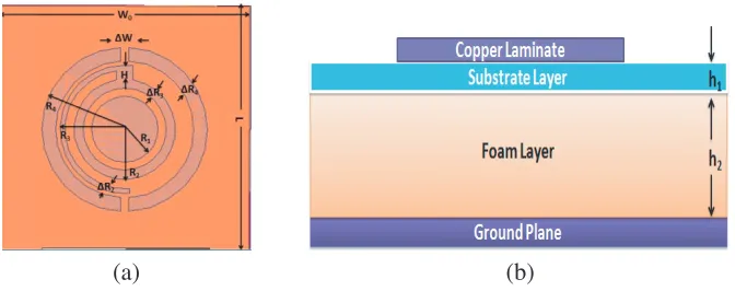
(a) (b)
2. PHASING ELEMENT CONFIGURATION AND DESIGN PROCEDURE
The proposed phasing element is designed to operate at a center frequency of 11.5 GHz and bandwidth 1 GHz. The proposed phasing element is shown in Fig. 1. It consists of a circular ring of radius R2 loaded by a circular disc microstrip patch of radiusR1. A phase-delay line of radiusR3 and width ΔR3 is attached to the circular ring through a notch of height H. The electrical length of the phase-delay line is Φs. Finally, an outer circular ring of radius R4 and width ΔR4 with a pair of gaps of width ΔW is surrounding the inner ring. The element is supported by a thin substrate of Rogers RT/Duroid 5880 with thickness h1 = 0.508 mm and relative permittivity εr1 = 2.2. A grounded thick foam layer of thickness h2 = 3.175 mm and relative permittivity εr2 = 1.06 is used to support this substrate. This low dielectric constant layer is used to reduce the slope of the reflection phase characteristic so that the operational bandwidth is increased. The dimension of the unit cell is chosen to be W0 =L= 15 mm, which is equivalent to 0.58λ0 at the center frequency.
The design steps for the phasing element are as follows.
1) The equivalent relative permittivity and total thickness of the two substrates are given by [17].
εrt =
N
n=1 hn rn
−1
·
N
n=1 hn
(1a)
ht = N
n=1
hn (1b)
2) The radius of a circular disc microstrip patch at the center frequency (fc) is obtained by [11]
R2 = F
1 + 2ht πεrtF
Ln
πF 2ht
+ 1.7726
1/2 (2)
F = 8.791×10 9
fc√εrt (3)
3) A phase-delay line with a notch is attached to a circular disc microstrip patch. By changing the dimensions ofR1, ΔR2, ΔR3 and H, a proper matching is obtained for different Φs at the central frequency 11.5 GHz. It should be noted that if there is a mismatch between the circular disc microstrip patch and the phase-delay line, then the relationship between phase response and Φsis no longer linear. 4) The final dimension of the phasing element is obtained by optimizing the phasing element geometrical parameters by using CST Microwave studio software.
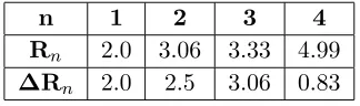
Table 2 gives the final optimized parameters that attain the linear reflection phase curve for the unit cell at the operating bandwidth.
Table 2. Optimized parameters of phasing element.
n 1 2 3 4
Rn 2.0 3.06 3.33 4.99
ΔRn 2.0 2.5 3.06 0.83
For the three simulation examples, isolated, identical, and non-identical, only one unit cell is
illuminated by a normally incident Gaussian beam of sinusoid waveform, and the scattered field ES and total fieldEtot are stored within a solid box sensor enclosing the two unit cells (collection volume) assuming that the neighboring unit cell is located at a distanced= (∞,15,15) mm, respectively.
The perturbation factors (εidentical(d), εnon identical(d)) are calculated for the identical and non-identical unit cells as in [16]
P F1 = εidentical(d) =Etot(d)−Etot(∞) (4a) P F2 = εnon identical(d) =Etot(d)−Etot(∞) (4b)
whereP F1 and P F2 are the perturbation factors for identical and non-identical unit cells, andEtot(d) and Etot(∞) denote the total fields for the surrounded and isolated cases, respectively. The field perturbation factor is directly related to the mutual coupling since it measures the variation induced by the reradiated field from the neighboring unit cell. Equation (8b) in [16] relates the perturbation factor to the mutual coupling where it includes the modification of parametersS11of illuminating unit cell and S21 of surrounded unit cell in a way to quantify the coupling effect in terms of field strength. The perturbation technique provides an equivalent way of calculating the mutual coupling of classical array configurations.
Figure 2 represents the comparison between P F1 and P F2 as a function of d at 11.5 GHz. It confirms that the effect of mutual coupling between neighboring unit cells is negligible for the proposed phasing element.
Figure 3 shows the phase response of the reflected wave for normal incidence with respect to Φs for different frequencies in the range 11.0 ∼12.0 GHz. The results indicate a linear phase response in the range 11.0∼12.0 GHz. It can be noted that by changing Φs up to 180◦, the phase range at each of the chosen frequencies exceeds 425◦, and at higher frequency the gradient is less than steep.
Figure 4 shows the phase of the reflected wave with respect to Φs for different angles of incidence (θ and φ). It shows that linear phase response and range of phase variation is almost constant for the incident angle up to 40◦. The results show that the phase performances for oblique incidence in different principal planes (φ= 0◦, 30◦, 40◦) are close. These characteristics make the proposed element a suitable choice for large-size reflectarrays. These phasing characteristics are the basis for obtaining an increased operational bandwidth of reflectarrays. Linear phase response and range of phase variation is almost constant for the incident angle up to 40◦ (the maximum phase difference with respect to normal incidence is 55◦ at Φs= 20◦ forφ= 40◦ and θ= 15◦.
-1 -1 -1 -1 -1 -1 Pert u rb a ti o n F a c to r (P F ) d B 15 150 140 130 120 110 100 -90 -80 -70 -60 20 25 Coupling di 30 3
stance (d) mm
35 40 45
PF2 (dB) PF1 (dB)
3. MEASUREMENT SETUP
For a validation of the simulation results for the reflected phase response curve, a C-band tapered waveguide section 4550-31BM1 with a dimension given in Table 3 is connected at one end with two identical unit cells as shown in Fig. 5, and the other end is connected to vector network analyzer model number 8719ES using an coaxial to waveguide adapter as shown in Fig. 6.
Table 3. Dimension of tapered waveguide section.
Model Number WG name A (mm) B (mm)
4550 WR-137 34.84 15.79
0 20 40 60 80 100 120 140 160 180
-500 -450 -400 -350 -300 -250 -200 -150 -100 -50 0
Φs (deg)
R
e
fl
ec
ti
o
n
pha
se
(d
eg
)
11.0 GHz 11.5 GHz 12.0 GHz
Figure 3. Phase of the reflection coefficient for normal incidence at different frequencies.
0 20 40 60 80 100 120 140 160 180
-500 -450 -400 -350 -300 -250 -200 -150 -100 -50 0
Φs (deg)
R
efl
ecti
o
n
pha
se
(deg
)
θ = 0o, φ = 0o
θ = 10o, φ = 30o θ = 20o, φ
φ = 0o θ = 15o, = 40o
Figure 5. Geometry of the designed two-patch element unit cell reflectarray.
Figure 6. Measurement setup for scattering element unit cell reflectarray. parameters measurements, Reprint [16].
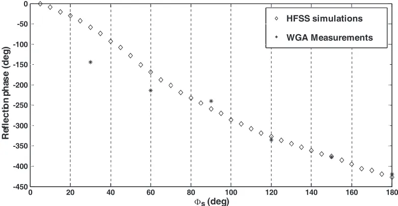
Figure 7. Fabricated samples of reflectarrays at different Φs= 30◦, 60◦, 90◦, 120◦, 150◦, 180◦.
0 20 40 60 80 100 120 140 160 180
-450 -400 -350 -300 -250 -200 -150 -100 -50 0
s (deg)
R
efl
ecti
o
n p
h
a
s
e (deg
)
HFSS simulations
WGA Measurements
Φ
Measurements are carried out on six fabricated sets of reflectarray unit cells to obtain six discrete points of reflection phase response. These elements sets have different phases for the corresponding reflected fields, 30◦, 60◦, 90◦, 120◦, 150◦ and 180◦.
4. MEASURED RESULTS AND DISCUSSION
The measurement procedure in [18] is carried out on fabricated sets of antenna elements as depicted in Fig. 7. The results are compared with the simulated results obtained by Ansoft HFSS software. Fig. 8 shows the simulated and measured reflection phase curves for different Φs. The presented results show that the reflection phase response has a sufficient range around 440◦. It has a linear variation which shows good overlap with the measured phase samples. At lower values of Φs, there is a discrepancy due to the use of C-band tapered waveguide section in measurement setup which controls the incident angle of inbound wave. For smaller values of oblique incidence in Fig. 4, the reflection phase values are affected.
5. CONCLUSION
New phasing element for reflectarray is proposed. This element is composed of a phase-delay line attached to a circular ring loaded by a circular disc microstrip patch. It is found to be suitable to achieve 440◦ linear phase range at central frequency 11.5 GHz. A field perturbation technique using FDTD technique is used to determine the mutual coupling between the nearby elements. Experimental results show the validity of the proposed phasing element in wideband applications.
ACKNOWLEDGMENT
The authors would like to thank Hesham Yamni (Electronics Research Institute) for his assistance in performing the measurements.
REFERENCES
1. Huang, J. and J. A. Encinar,Reflectarray Antenna, John Wiley & Sons, Ltd, 2007.
2. Carrasco, E., J. A. Encinar, and M. Barba, “Wideband reflectarray antenna using true-time delay lines,” The Second European Conference on Antennas and Propagation, EuCAP 2007, 1– 6, Edinburgh, 2007.
3. Carrasco, E., J. A. Encinar, and M. Barba, “Bandwidth improvement in large reflectarrays by using true-time delay,” IEEE Transactions on Antennas and Propagation, Vol. 56, No. 8, 2496– 2503, Aug. 2008.
4. Bozzi, M., S. Germani, and L. Perregrini, “Performance comparison of different element shapes used in printed reflectarrays,” IEEE Antennas and Wireless Propagation Letters, Vol. 2, No. 1, 219–222, 2003.
5. Bialkowski, M. E. and K. H. Sayidmarie, “Investigations into phase characteristics of a single-layer reflectarray employing patch or ring elements of variable size,” IEEE Transactions on Antennas and Propagation, Vol. 56, No. 11, 3366–3372, Nov. 2008.
6. Ismail, M. Y., M. F. B. M. Shukri, Z. Zakaria, A. F. M. Zain, M. F. L. Abdullah, and M. A. Ubin, “Investigation of static phasing distribution characteristics of passive reflectarray antenna elements,” PIERS Proceedings, 1218–1222, Moscow, Russia, Aug. 18–21, 2009.
7. Misran, N., R. Cahill, and V. F. Fusco, “Design optimisation of ring elements for broadband reflectarray antennas,”IEE Proceedings — Microwaves, Antennas and Propagation, Vol. 150, No. 6, 440–444, Dec. 2003.
9. Sayidmarie, K. H. and M. E. Bialkowski, “Phasing of a microstrip reflectarray using multi-dimensional scaling of its elements,” Progress In Electromagnetics Research B, Vol. 2, 125–136, 2008.
10. Li, Y., M. E. Bialkowski, K. H. Sayidmarie, and N. V. Shuley, “81-element single-layer reflectarray with double-ring phasing elements for wideband applications,” 2010 IEEE Antennas and Propagation Society International Symposium, 1–4, Toronto, ON, 2010.
11. Malfajani, R. S. and Z. Atlasbaf, “Design and implementation of a broadband single-layer reflectarray antenna with large-range linear phase elements,” IEEE Antennas and Wireless Propagation Letters, Vol. 11, 1442–1445, 2012, doi: 10.1109/LAWP.2012.2228147.
12. Hasani, H., M. Kamyab, and A. Mirkamali, “Broadband reflectarray antenna incorporating disc elements with attached phase-delay lines,” IEEE Antennas and Wireless Propagation Letters, Vol. 9, 156–158, 2010, doi: 10.1109/LAWP.2010.2044473.
13. Han, C., Y. Zhang, and Q. Yang, “Single-layer reflectarray antennas with improved bandwidth by attaching phase-delay lines,” Proceedings of the 10th European Conference on Antennas and Propagation (EUCAP), 1–4, Davos, 2016.
14. Li, Y. and M. E. Bialkowski, “Investigations into electronically controlled rings with arc stubs phasing elements for reconfigurable microstrip reflectarrays,” Asia-Pacific Microwave Conference 2011, 943–946, Melbourne, VIC, 2011.
15. Li, Y., M. E. Bialkowski, and A. M. Abbosh, “Single layer reflectarray with circular rings and open-circuited stubs for wideband operation,” IEEE Transactions on Antennas and Propagation, Vol. 60, No. 9, 4183–4189, Sept. 2012, doi: 10.1109/TAP.2012.2207060.
16. Jamaluddin, M. H., R. Gillard, and R. Sauleau, “Perturbation technique to analyze mutual coupling in reflectarrays,” IEEE Antennas and Wireless Propagation Letters, Vol. 8, No. 1, 697–700, 2009. 17. Ali, W. K. W. and S. H. Al-Charchafchi, “Using equivalent dielectric constant to simplify
the analysis of patch microstrip antenna with multi-layer substrates,” IEEE Antennas and Propagation Society International Symposium, 1998, Vol. 2, 676–679, Atlanta, GA, USA, 1998, doi: 10.1109/APS.1998.702028.