ABSTRACT
ZHANG, XU. Functional Three-Dimensional Nanostructures Using Colloidal Particles. (Under the direction of Dr. Chih-Hao Chang).
The refractive indices of naturally occurring materials are limited, and there exists an index gap between indices of air and available solid materials. With many photonics and electronics applications, there has been considerable effort in creating artificial materials with optical and dielectric properties similar to air while simultaneously being mechanically stable to bear load. In the second part of this dissertation, I demonstrated a class of ordered nanolattice materials consisting of periodic thin-shell structures with near-unity refractive index and high stiffness. Using a combination of 3D nanolithography and atomic layer deposition, these ordered nanostructured materials have reduced optical scattering and improved mechanical stability compared to existing randomly porous materials. Using ZnO and Al2O3 as the building materials, refractive indices from 1.3 down to 1.025 were achieved. The experimental data can be accurately described by Maxwell-Garnett effective media theory, which can provide a guide for index design. The demonstrated low-index, low-scattering, and high-stiffness materials can serve as high-quality optical films in multilayer photonic structures, waveguides, resonators, and ultra-low-k dielectrics.
Functional Three-Dimensional Nanostructures Using Colloidal Particles
by Xu Zhang
A dissertation submitted to the Graduate Faculty of North Carolina State University
in partial fulfillment of the requirements for the degree of
Doctor of Philosophy
Mechanical Engineering
Raleigh, North Carolina 2016
APPROVED BY:
_______________________________ _______________________________ Dr. Gregory Parsons Dr. Yong Zhu
_______________________________ _______________________________ Dr. Orlin Velev Dr. Xiaoning Jiang
_______________________________ Dr. Chih-Hao Chang
BIOGRAPHY
ACKNOWLEDGMENTS
I want to thank my advisor, Dr. Chih-Hao Chang, who has given me not only the most professional academic training, but also valuable career and life advice by setting up a good role model as a family person as well as a devoted researcher. I benefit quite much from his different views about problems. Luckily being among his first students, I was able to learn everything from the start. I will never forget his “Research is fun.” And I hope to pass it along to my future students.
I want to thank soon-to-be Dr. Abhijeet Bagal, Jonathan Elek, Joong Hee Min, and Wei-Yi Chang for the happy days and nights in the lab. The discussions were always helpful and enlightening. Thanks to the many graduate and undergraduate students for bringing interesting ideas and helping with my research, including Zhiren Luo, Sharan Vinod Naidu, Jonathan Chu, Austen Poteet, Hironori Nagai, Jared Tippens, Zhiyuan Xu, Bin Dai and Travis Rivord.
I want to thank my beloved parents for paving the way of my current amazing life when I was unable to make life decisions at young ages. I thank for their constant supports and preparing me for bigger challenges in life by cultivating my independent thinking and sense of responsibility. I also want to thank my fiancée, Yue Li, for always being on my side and dragging me out of life confusions. Her companion and support made the life abroad easier.
TABLE OF CONTENTS
LIST OF TABLES ... vii
LIST OF FIGURES ... viii
CHAPTER 1 INTRODUCTION ... 1
1.1 Applications of 3D Nanostructures ... 2
1.1.1 Bio-Inspired Functionalities ... 2
1.1.2 Photonics Applications ... 5
1.1.3 Energy Applications ... 6
1.1.4 Biomedical Applications ... 8
1.2 Fabrication Techniques of 3D Nanostructures ... 9
1.2.1 “Top-Down” Techniques ... 10
1.2.2 “Bottom-Up” Techniques ... 13
1.2.3 Combining “Top-Down” and “Bottom-Up” Techniques... 15
1.3 Dissertation Structure ... 19
CHAPTER 2 LIGHT SCATTERING THEORY ... 21
2.1 Mie Theory ... 24
2.1.1 Field Solutions ... 24
2.1.2 Cross Sections and Efficiencies ... 31
2.2 Rayleigh Theory ... 33
2.3 Light Scattering Intensity Distributions ... 34
2.4 Summary ... 36
CHAPTER 3 COLLOIDAL PARTICLE SELF-ASSEMBLY TECHNIQUES ... 37
3.1 Molecular Self-Assembly ... 38
3.2 Mechanism of Colloidal Particle Self-Assembly ... 39
3.3 Ordered Particle Self-Assembly Techniques ... 40
3.3.1 Colloidal Self-Assembly by Drop Casting ... 40
3.3.3 Colloidal Self-Assembly on Air/Water Interfaces ... 49
3.3.4 Binary Colloidal Crystals ... 52
3.3.5 Templated-Directed Self-Assembly ... 53
3.4 Isolated Particle Assemblies with Random Order ... 54
3.5 Summary ... 56
CHAPTER 4 THREE-DIMENSIONAL NANOLITHOGRAPHY USING COLLOIDAL PARTICLES — NORMAL INCIDENCE ... 58
4.1 Fabrication Concept ... 59
4.2 Structure Modelling and Prediction ... 61
4.3 Single Nano-Volcanoes ... 64
4.4 Fabrication of Nano-Volcano Arrays ... 72
4.5 Application as Drug Delivery Surfaces ... 75
4.6 Plasmonic Metal Particles for Subwavelength Patterning: A Simulation Analysis 81 4.7 Summary ... 85
CHAPTER 5 THREE-DIMENSIONAL NANOLITHOGRAPHY USING COLLOIDAL PARTICLES — OBLIQUE INCIDENCE ... 86
5.1 Fabrication Concept ... 87
5.2 FDTD Simulation and Binary Resist Model ... 89
5.3 Fresnel Transmission ... 90
5.4 Fabrication Results with Single Oblique Exposure ... 91
5.5 Multiple Exposures ... 98
5.6 Fabrication of Arrays and Anisotropic Wetting Properties ... 108
5.7 Summary ... 112
CHAPTER 6 AIR-LIKE NANOLATTICE MATERIALS ... 113
6.1 Background ... 113
6.2 Effective Medium Theory ... 119
6.3 Fabrication Strategy ... 122
6.5 Numerical Model and Solid Fraction Calculation ... 129
6.6 Ellipsometry Measurements and Fitting Strategies ... 131
6.7 Refractive Index Characterization and Modellings ... 132
6.8 Scattering Characteristics ... 138
6.9 Integration of Nanolattice Materials ... 141
6.10 Summary ... 144
CHAPTER 7 MAGNETICALLY TUNABLE NANOSTRUCTURES ... 145
7.1 Venetian Blind Model for Color Tuning ... 148
7.2 Magnetic Actuation Mechanisms ... 149
7.3 Research Goal ... 154
7.4 Fabrication of Magnetically Tunable Nanostructures and Actuation Tests ... 156
7.5 Magnetically Tunable Nanostructures Integration with Microelectromagnets ... 161
7.6 Summary ... 166
CHAPTER 8 CONCLUSION... 167
LIST OF TABLES
LIST OF FIGURES
Figure 1-1. (a) Antireflective nanostructures of moth eye [1]. (b) Directional dry adhesive nanostructures [2]. (c) Structural color of butterfly wings [1]. (d) Directional wetting of
butterfly wings [7]... 3
Figure 1-2. Multifunctional glass [13]. (a) Nanocone structures. (b) Multifunctionalities of nanocone structures. ... 4
Figure 1-3. (a)-(c) Polymer photonic crystal fabricated with four-beam interference. (d) Transmittance and reflectance spectra of the fabricated photonic crystal [16]. ... 6
Figure 1-4. (a) Schematic of a battery containing a bicontinuous cathode. (b) SEM images of 3D bicontinuous battery electrodes [24]. ... 7
Figure 1-5. (a) On-demand releasing mechanism of drug delivery using nanocages. (b-c) Nanocages before and after drug loading, respectively [27]. ... 8
Figure 1-6. Multiple beam interference lithography [38]. ... 11
Figure 1-7. Phase-shift lithography process [42]. ... 12
Figure 1-8. 3D nanostructures by colloidal particle self-assembly [45]. ... 14
Figure 1-9. Colloidal lithography using colloidal particle assemblies as deposition masks [54], [55]. ... 16
Figure 1-10. Three-dimensional nanolithography using colloidal particle phase masks [60]. (a) Fabrication principles. (b) SEM images of fabricated 3D nanostructures. ... 17
Figure 1-11. 2D surface patterning using light scattering of single colloidal particles [63]. . 18
Figure 2-1. Photograph taken during a sunny day at Raleigh, NC. The blue sky and the white clouds are perfect presentations of the results of Rayleigh and Mie scatterings. ... 21
Figure 2-2. Interpretation of scattering mechanism [65]. ... 23
Figure 2-3. Light scattering problem diagram. ... 25
Figure 2-4. Field lines of total Poynting vector excluding scattered light near a small Al sphere [66]. ... 32
Figure 2-5. (a) Rayleigh intensity pattern for single particle with 10 nm radius and 325 nm wavelength. (b) Mie scattering intensity pattern for 250 nm radius particle and 325 nm wavelength. Only forward total intensity distributions are calculated in air. Particles are not drawn in scale. ... 35
wavelength laser. Scale bars represent 1 μm in (a), (d) and (g), and 500 nm in (b), (c), (e) and
(f)... 127
Figure 6-6. Scanning electron micrographs of nanolattice materials with Al2O3 shell thicknesses of (a) 2.1 nm; (b) 4.0 nm; (c) 9.2 nm; (d) 16.3 nm and ZnO shell thicknesses of (e) 21.3 nm; (f) 31.5 nm. Scale bars: 1 μm. ... 128
Figure 6-7. (a) One cross section of the 3D intensity pattern created by nanosphere arrays and UV illumination. (b) Structure prediction using binary resist model. A unit cell is shown. 130 Figure 6-8. Ellipsometry measurement data with model fitting using Sellmeier-type material dispersion and three-layer optical model. ... 132
Figure 6-9. Measured broadband refractive indices for various nanolattices with different material composition and shell thicknesses. (a) Index of Al2O3 samples with different thicknesses. Colored region shows the index bounds for 19.0 nm lattice using first-order effective medium approximation. (b) Index of ZnO samples with different thicknesses. Colored region shows the index bounds for 21.3 nm lattice using first-order effective medium approximation. ... 133
Figure 6-10. Angle dependence of nanolattice dispersions. ... 135
Figure 6-11. Nanolattices with 58.0 nm ZnO ALD coating. ... 136
Figure 6-12. Normalized material property, β, versus solid volume fraction, f. The analytical model plotted is based on Maxwell Garnett effective medium theory. The experimental data are indices at 633 nm wavelength for all the samples. ... 137
Figure 6-13. Angular measurement setup for characterizing angular scattering profile. ... 138
Figure 6-14. (a) Specular transmission and light scattering properties of the fabricated low-index nanolattice materials. The specular transmission of glass is plotted for comparison. (b) Photographs of fabricated sample and bare glass. “NM” is the nanolattice material with 15.2 nm Al2O3 shells. A tablet screen was used as a backlit background. ... 139
Figure 6-15. (a) FDTD simulation setup for 56.7º incident angle. (b) A snapshot of the field distributions from the FDTD simulation setup in (a). (c) Transmission comparison between homogeneous film (n = 1.1) by T-matrix method and nanoaccordion structures (neff = 1.1) by FDTD simulation. The arrow indicates the data from FDTD simulation in (a) and (b). ... 142
Figure 6-16. Scanning electron microscope graphs showing the results of capping holes with secondary deposition of 15 nm planar Al2O3 film from atomic layer deposition. ... 143
Figure 7-1. Tunable colors of the chameleon skins caused by photonic crystals [137]. ... 146
Figure 7-2. Neon tetra color change by rotating platelets on the scales [138]. ... 146
Figure 7-4. Venetian blind model. (a) Zero rotation of reflecting platelets. (b) Reflecting platelets undertake rotation of θ and reflecting at peak wavelength λp. ... 149
CHAPTER 1 INTRODUCTION
the field by improving public recognitions of nanoscience and nanotechnology and bringing young talents to be future researchers.
Despite the vast scope of nanoscience and nanotechnology, substantial research efforts have been devoted to the subfield about nanostructures and nanostructured materials. It is impossible to cover all the aspects of various nanostructures in zero dimension (0D), one dimension (1D), two dimensions (2D) and three dimensions (3D). In particular, I will introduce specifically about 3D nanostructures regarding their applications and fabrication techniques in this chapter. The applications of 3D nanostructures will be briefly introduced in the areas of bio-inspired functionalities, photonics, energy, and biomedical engineering among other areas, and then a review of 3D manufacturing techniques will be given.
1.1 Applications of 3D Nanostructures 1.1.1 Bio-Inspired Functionalities
capability of geckos is solely due to the hierarchical structures of microscale setae and nanoscale spatulae, as shown in Figure 1-1(b) [2]. The adhesion is due to van der Waals force and is directional by the angular alignments of the structures [3], [4]. Self-cleaning capabilities have also been discovered from the same structures [2]. Gecko’s foot serves as an excellent example of multifunctionalities in nature’s design. Another example is the butterfly wing, where the complex hierarchical periodic structures give the brilliant color due to diffraction, as well as the ability to shed water directionally at the same time, as shown in Figure 1-1(c) and (d) [5]–[7].
Figure 1-1. (a) Antireflective nanostructures of moth eye [1]. (b) Directional dry adhesive nanostructures [2]. (c) Structural color of butterfly wings [1]. (d) Directional wetting of butterfly
Considerable research has been conducted to mimic the bio-inspired functionalities shown before, thanks to the rapid progress of advanced nanofabrication techniques. Engineered dry adhesive structures range from microscale pillars by replication techniques [8], [9] to the true resemblance of the hierarchical gecko foot structures by soft lithography and dry etching [10]. Structural colors with butterfly wing-type structures have also been studied extensively and realized by dry and wetting etching techniques [11]. Engineered multifunctional nanocone structures have been realized using replication and etching techniques [12]–[15]. The nanocones structures show capabilities of enhanced optical transmission, anti-fogging, superhydrophobicity and self-cleaning, as shown in Figure 1-2.
1.1.2 Photonics Applications
Figure 1-3. (a)-(c) Polymer photonic crystal fabricated with four-beam interference. (d) Transmittance and reflectance spectra of the fabricated photonic crystal [16].
1.1.3 Energy Applications
particle self-assemblies, as shown in Figure 1-4 [24]. The interconnected 3D pore network enables rapid ion transport and a large electrode surface area, leading to ultrafast, supercapacitor-like discharge and charge rate capability while maintaining battery-like large storage capacities.
1.1.4 Biomedical Applications
Three-dimensional hollow nanostructures have found important applications in drug delivery systems with the capability to load and release drugs with nanoscale-volume precision to prevent overdose [25]–[28]. An interesting class of hollow nanostructures called nanocages have attracted researchers due to their capability of achieving on-demand drug release either by infrared illumination or heating [26], [27]. In Figure 1-5, the mechanism of thermal drug release is depicted for nanocages with the help of phase change materials (PCM) as drug loading medium. Drug molecules are naturally locked inside the nanocages below the melting point of the PCM. Release occurs when the temperature is above the melting point through molecular diffusion. Other than drug delivery applications, 3D nanostructures can also interact with biological cells for the study of cell behaviors under different topologies. Now the so-called “three-dimensional nano-biointerfaces” provide a novel platform to guide cell fate in a controllable and accurate way, bringing a series of new phenomena and developments of cell-related fundamental biological studies and advanced biomedical applications [29].
1.2 Fabrication Techniques of 3D Nanostructures
1.2.1 “Top-Down” Techniques
Various “top-down” 3D lithography approaches have been used to enable 3D nanostructures for the aforementioned applications and they are mostly based on optical lithography. Using conventional 2D planar lithography and etching techniques, photonic crystals such as woodpile structures can be achieved by a layer-by-layer approach [30], [31]. Arbitrary complex 3D nanostructures can be achieved using focused ion beam (FIB) [32] and electron-beam lithography [33]. One particular effective 3D patterning technique that has drawn significant research interest is direct-write two-photon polymerization, which allows pattering of arbitrary structures in 3D space [34]–[37]. However, since this is inherently a serial process where focused light is scanned across the sample to expose individual voxels, the write time increases significantly for large areas. This technique also requires elaborate system hardware including ultrafast pulsed lasers, scanning optics, and feedback controls electronics. While the above techniques are effective in creating complex structures, they can be costly and difficult to scale up for manufacturing because of the serial processing nature.
inverse problem of beam configurations with given 3D geometries, and the method is described in a book by Professor Edwin L. “Ned” Thomas, based on spatial Fourier transforms of the target 3D geometry [40]. However, this technique relies on elaborate systems to finely tune each beam’s properties, which is not a trivial task. Moreover, the fabrication area is limited to the overlaid regions of the multiple beams, and large-area fabrications are hardly practical since each beam needs to be expanded, resulting in significant nonuniformities of beam intensity.
Figure 1-6. Multiple beam interference lithography [38].
nanostructures are revealed after development. The 3D photoresist nanostructures can latter serve as template for replicating inverse structures with other materials. This technique requires a single flood exposure, resulting in 3D lithography with high throughput and scalability, and the resolution of this technique is in the order of the exposure wavelength. However, there has been no direct design method for the phase masks to achieve specific types of 3D nanostructures, and the fabrication of the phase masks sometimes has to adopt the serial fabrication methods discussed before, although parallel processes such as interference lithography can also be utilized.
1.2.2 “Bottom-Up” Techniques
Figure 1-8. 3D nanostructures by colloidal particle self-assembly [45].
before that age to come, there are still a lot of questions to be answered regarding the physics and mechanisms of natural assembly processes. Another major problem in colloidal self-assembly is the formation of defects in colloidal assemblies, such as grain boundaries, vacancies and dislocations. One example of 2D colloidal assembly will be given in Chapter 3 to illustrate the defects. The defect formation is an extremely complicated process, which is often related to various factors such as colloidal particle size distribution, particle shape, temperature, humidity, and surface chemistry. Typically, 2D assemblies have less defects and larger grains than 3D assemblies due to the relatively simpler assembly process. Therefore, 2D colloidal particle self-assembly techniques and their use in 3D nanolithography are investigated in this dissertation.
1.2.3 Combining “Top-Down” and “Bottom-Up” Techniques
such as hemispherical metal caps [57], nanopores [58], and sculptured colloids [51] with relatively low costs.
Figure 1-9. Colloidal lithography using colloidal particle assemblies as deposition masks [54], [55].
phase-shift lithography described in the previous sections, but in this case self-assembled nanospheres are employed as integrated phase elements. The approach eliminates mask fabrication costs and avoids close-contact issues often seen in conventional mask lithography techniques.
Colloidal particle arrays are used in the above techniques, but one may ask what can happen if only single particles are used in this technique. Light interaction with single particles is the light scattering effect, and some work has been performed within the realm of 2D surface patterning [61]–[63]. As shown in Figure 1-11, oblique incidence on colloidal particles can generate complex ripple-like structures on 2D surface [63]. In another approach, highly focused light by a single particle lens can be manipulated using optical trap to write arbitrary patterns on solid surface [62]. However, existing work is limited to 2D surface patterning while light scattering is essentially a three-dimensional effect. In this dissertation, the exploration of novel 3D nanolithography techniques using light scattering from single particles will be described in latter chapters.
1.3 Dissertation Structure
In this dissertation I will present my research on the fabrication and study of 3D nanostructures in the following structure. In Chapter 2, a brief overview of light scattering theory by spherical particles is given. The exact solution of scattering problems are derived according to the Mie theory. The comparison between Mie and Rayleigh theories is discussed and provides the theoretical foundation for the novel 3D nanolithography using light scattering principles.
In Chapter 3, more discussions on the mechanisms and various techniques of colloidal self-assembly are provided. The review is not necessarily complete and thorough due to the highly active research in this area, but basic self-assembly techniques, such as drop casting, assembly by substrate withdrawal and air/water interfaces, are described in details, including custom-built setups for these techniques during my doctoral research. Other types of assembly orders such as binary assemblies and isolated single particles, are also achieved.
parameters, such as incident angle, polarization states, and arrangement of multiple illuminations.
Chapter 6 describes a novel 3D nanostructured material with periodic order to precisely tailor the refractive index using a combination of atom layer deposition (ALD) and 3D nanolithography technique. In this work, I demonstrated near-unity index of 1.025, which is the lowest thin-film index ever reported, and these ordered three-dimensional nanostructured materials can be accurately designed. As opposed to randomly ordered materials, the periodic nanolattice materials possess three key advantages of designable refractive index, enhanced mechanical stiffness, and reduced scattering. I also demonstrated that by engineering the lattice geometry and material composition, low-index materials with indices from 1.025 to 1.3 can be accurately designed to completely fill the naturally-occurring refractive index gap.
CHAPTER 2
LIGHT SCATTERING THEORY
The study of light scattering was driven by the curiosity of scientists such as Lord Rayleigh, Gustav Mie, Ludvig Lorenz and so on, who would not take natural phenomena for granted [64]. The particular phenomenon that caught their attentions is the colors of sky and clouds, which show distinct contrast of blue and white on the sky. When developing this chapter, I took a photograph of the sky during a sunny day to show the outstanding color contrast outside Engineering Building III of North Carolina State University at Raleigh, North Carolina, as shown in Figure 2-1. Lord Rayleigh proposed that the blue color of the sky is a result of light scattering by the extremely small molecules in air. The scattered light intensity scales with the inverse fourth power of the wavelength, leading to strong scattering for short wavelengths which human eyes perceive as blue. The white color from the clouds, however, is due to the light scattering by large particles, such as water droplets in the clouds, and can be described accurately by Mie theory. It turns out that large particles scatter light relatively equally for different wavelengths or colors so that the clouds exhibit white color.
Figure 2-2. Interpretation of scattering mechanism [65].
2.1 Mie Theory 2.1.1 Field Solutions
The problem of light scattering by single spheres can be solved exactly using Maxwell’s equations under the framework of classical electrodynamics. The four elegant equations are listed below,
∇ ∙ 𝑫 = 𝜌
∇ × 𝑬 = −𝜕𝑩 𝜕𝑡 ∇ ∙ 𝑩 = 0
∇ × 𝑯 = 𝑱 +𝜕𝑫 𝜕𝑡
where E is the electric field, B is the magnetic induction, J is the current density, and ρ is the free charge. The electric displacement D and magnetic field H are defined by the following relations,
𝑫 = 𝜀0𝑬 + 𝑷
𝑩 = 𝜇0(𝑯 + 𝑴)
where P and M are the electric polarization and magnetization of the material, and ε0 and μ0
are the permittivity and permeability of vacuum.
The constituent relations are supplemental to solving Maxwell’s equations,
𝑱 = 𝜎𝑬
𝑩 = 𝜇𝑯
where σ is the electric conductivity, µ is the permeability, and χ is the electric susceptibility. Here the material is assumed to be linear, homogeneous and isotropic.
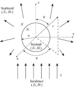
For light scattering by single particles, the free charge and current density are assumed to be zeros for most of the cases. The problem to solve is illustrated in Figure 2-3. A sphere with radius a and complex refractive index N1 is situated in an otherwise homogeneous medium
with complex refractive index N. The sphere is illuminated by an infinitely wide x-polarized light with wavelength λ and electromagnetic fields of (Ei, Hi) propagating in the z direction.
The incidence is scattered to all directions with scattered fields, (Es, Hs), to be solved. The
internal fields are denoted as (El, Hl). Maxwell’s equations are solved in spherical coordinates,
In general, the sphere can be illuminated by electromagnetic waves with arbitrary wavelengths and amplitudes. However, only the solutions under the incidence of time harmonic fields are needed since any illumination can be regarded as the Fourier series expansion of the time harmonic fields. Due to the linearity of Maxwell’s equations, the solutions to arbitrary incidence can be the superpositions of the solutions under Fourier components.
The time harmonic fields need to satisfy the Helmholtz equations derived from the Maxwell’s equations,
∇2𝑬 + 𝑘2𝑬 = 0, ∇2𝑯 + 𝑘2𝑯 = 0
𝑬 = 𝐸0exp [𝑖(𝒌 ∙ 𝒓 − 𝜔𝑡], 𝑯 = 𝐻0exp [𝑖(𝒌 ∙ 𝒓 − 𝜔𝑡]
where k = |k| = 2π/λ = ω(εμ)-1/2. In addition, the electric and magnetic fields are related by,
∇ × 𝑬 = 𝑖𝜔𝜇𝑯, ∇ × 𝑯 = −𝑖𝜔𝜀𝑬.
The boundary conditions on the surface of the sphere state that the tangential components of electric and magnetic fields are continuous,
[(𝑬𝑖 + 𝑬𝑠) − 𝑬𝑙] × 𝒓̂ = 0
[(𝑯𝑖+ 𝑯𝑠) − 𝑯𝑙] × 𝒓̂ = 0
where 𝒓̂is the surface normal of the sphere or the unit vector of r.
the above vector differential equations to scalar differential equations, which are easier to solve. The vector functions are constructed as below,
𝑴 = ∇ × (𝒓𝜓)
𝑵 =∇ × 𝑴
𝑘
The vector functions M and N satisfy the above Helmholtz equations except for M,
∇2𝑴 + 𝑘2𝑴 = ∇ × [𝒓(∇2𝜓 + 𝑘2𝜓)].
Therefore, M satisfies the wave equations as long as the following scalar differential equation is solved,
∇2𝜓 + 𝑘2𝜓 = 0.
The solutions to the above scalar differential equation is achieved by separation of variables for decomposition into orthogonal modes and are listed below,
𝜓𝑒𝑚𝑛 = cos 𝑚𝜑 𝑃𝑛𝑚(cos 𝜃)𝑧
𝑛(𝑘𝑟) (even mode)
𝜓𝑜𝑚𝑛 = sin 𝑚𝜑 𝑃𝑛𝑚(cos 𝜃)𝑧
𝑛(𝑘𝑟) (odd mode) where zn is any of the following four spherical Bessel functions,
𝑗𝑛(𝑘𝑟) = √ 𝜋
2𝑘𝑟𝐽𝑛+12(𝑘𝑟) 𝑦𝑛(𝑘𝑟) = √
𝜋
2𝑘𝑟𝑌𝑛+12(𝑘𝑟)
ℎ𝑛(1)(𝑘𝑟) = 𝑗𝑛(𝑘𝑟) + 𝑖𝑦𝑛(𝑘𝑟) ℎ𝑛(2)(𝑘𝑟) = 𝑗𝑛(𝑘𝑟) − 𝑖𝑦𝑛(𝑘𝑟)
Having solved the scalar ψ, now we can achieve the vector functions, 𝑴𝑒𝑚𝑛 = ∇ × (𝒓𝜓𝑒𝑚𝑛) 𝑴𝑜𝑚𝑛= ∇ × (𝒓𝜓𝑜𝑚𝑛) 𝑵𝑒𝑚𝑛 = ∇ × 𝑴𝑒𝑚𝑛 𝑘 𝑵𝑜𝑚𝑛 = ∇ × 𝑴𝑜𝑚𝑛 𝑘
which are called the vector spherical harmonics to form a complete orthogonal set of basis for field expansions.
Using the spherical vector harmonics, the incident plane wave can be expanded as,
𝑬𝑖 = ∑ 𝐸𝑛(𝑴𝑜1𝑛 (1)
− 𝑖𝑵𝑒1𝑛(1) )
∞
𝑛=1
𝑯𝑖 = −𝑘
𝜔𝜇∑ 𝐸𝑛(𝑴𝑒1𝑛
(1)
+ 𝑖𝑵𝑜1𝑛(1) )
∞
𝑛=1
where 𝐸𝑛 = 𝐸0𝑖𝑛 2𝑛+1
𝑛(𝑛+1) and the superscript (1) in M and N means jn is used for spherical vector
harmonics.
Both the unknown internal fields, (El, Hl), and the scattered fields, (Es, Hs), can be expanded
in similar forms,
𝑬𝑙 = ∑ 𝐸𝑛(𝑐𝑛𝑴𝑜1𝑛(1) − 𝑖𝑑𝑛𝑵𝑒1𝑛(1) )
∞
𝑛=1
𝑯𝑖 =
−𝑘𝑙 𝜔𝜇𝑙
∑ 𝐸𝑛(𝑑𝑛𝑴𝑒1𝑛 (1)
+ 𝑖𝑐𝑛𝑵𝑜1𝑛 (1)
)
∞
𝑛=1
𝑬𝑠 = ∑ 𝐸𝑛(𝑖𝑎𝑛𝑵𝑒1𝑛(3) − 𝑏𝑛𝑴𝑜1𝑛(3) )
∞
𝑯𝑠 =
𝑘
𝜔𝜇∑ 𝐸𝑛(𝑖𝑏𝑛𝑵𝑜1𝑛
(3)
+ 𝑎𝑛𝑴𝑒1𝑛 (3)
)
∞
𝑛=1
where the superscript (3) means M and N are expressed in terms of ℎ𝑛(1).
By matching the boundary conditions on the sphere surface and using the orthogonality of spherical vector harmonics, the coefficients an, bn, cn and dn can be derived. Therefore, the
internal and scattered fields can be achieved in explicit forms. The coefficients are expressed as follows,
𝑎𝑛 =
𝜇𝑚2𝑗
𝑛(𝑚𝑥)[𝑥𝑗𝑛(𝑥)]′− 𝜇𝑙𝑗𝑛(𝑥)[𝑚𝑥𝑗𝑛(𝑚𝑥)]′
𝜇𝑚2𝑗
𝑛(𝑚𝑥)[𝑥ℎ𝑛 (1)
(𝑥)]′− 𝜇𝑙ℎ𝑛(1)(𝑥)[𝑚𝑥𝑗𝑛(𝑚𝑥)]′
𝑏𝑛 = 𝜇𝑙𝑗𝑛(𝑚𝑥)[𝑥𝑗𝑛(𝑥)]
′− 𝜇𝑗
𝑛(𝑥)[𝑚𝑥𝑗𝑛(𝑚𝑥)]′
𝜇𝑙𝑗𝑛(𝑚𝑥)[𝑥ℎ𝑛 (1)
(𝑥)]′− 𝜇ℎ𝑛(1)(𝑥)[𝑚𝑥𝑗𝑛(𝑚𝑥)]′
𝑐𝑛 = 𝜇𝑙𝑗𝑛(𝑥)[𝑥ℎ𝑛
(1)
(𝑥)]′− 𝜇𝑙ℎ𝑛(1)(𝑥)[𝑥𝑗𝑛(𝑥)]′
𝜇𝑙𝑗𝑛(𝑚𝑥)[𝑥ℎ𝑛(1)(𝑥)]′− 𝜇ℎ𝑛(1)(𝑥)[𝑚𝑥𝑗𝑛(𝑚𝑥)]′
𝑑𝑛 = 𝜇𝑙𝑚𝑗𝑛(𝑥)[𝑥ℎ𝑛
(1)
(𝑥)]′− 𝜇𝑙𝑚ℎ𝑛(1)(𝑥)[𝑥𝑗𝑛(𝑥)]′
𝜇𝑚2𝑗
𝑛(𝑚𝑥)[𝑥ℎ𝑛 (1)
(𝑥)]′− 𝜇𝑙ℎ𝑛 (1)
(𝑥)[𝑚𝑥𝑗𝑛(𝑚𝑥)]′
with size parameter x, and refractive index contrast m defined as,
𝑥 = 𝑘𝑎 =2𝜋𝑁𝑎
𝜆 , 𝑚 = 𝑁1
𝑁.
2.1.2 Cross Sections and Efficiencies
Cross sections and efficiencies are quantitative parameters to describe scattering processes. There are scattering, absorption and extinction cross sections, which are defined as the ratios of the respective energy flow rate through a closed surface incorporating the entire sphere and the incident intensity,
𝐶𝑎 = 𝑊𝑎 𝐼𝑖 𝐶𝑠 = 𝑊𝑠 𝐼𝑖 𝐶𝑒𝑥𝑡 = 𝑊𝑒𝑥𝑡 𝐼𝑖
with unit of areas. The scattering, absorption and extinction efficiencies are defined as the ratios of the above cross sections and the geometrical area of the 2D projection of the sphere, which are expressed as follows,
𝑄𝑎 =
𝐶𝑎
𝜋𝑎2 𝑄𝑠 =
𝐶𝑠
𝜋𝑎2 𝑄𝑒𝑥𝑡 =
𝐶𝑒𝑥𝑡 𝜋𝑎2.
The cross sections are related as follows,
𝐶𝑒𝑥𝑡 = 𝐶𝑎+ 𝐶𝑠
𝑄𝑒𝑥𝑡 = 𝑄𝑎+ 𝑄𝑠.
With the coefficients an, bn, cn and dn, the cross sections can be expressed by the following
equations,
𝐶𝑠 =2𝜋
𝑘2 ∑(2𝑛 + 1)(|𝑎𝑛|
2+ |𝑏
𝑛|2) ∞
𝑛=1
𝐶𝑒𝑥𝑡 = 2𝜋
𝑘2 ∑(2𝑛 + 1)𝑅𝑒{𝑎𝑛+ 𝑏𝑛}. ∞
There is an interesting result based on the above definition of efficiencies: scattering efficiency can be over 100% at certain illumination wavelengths; in other words, a particle can absorb more than the light incident on it. Bohren wrote an interesting paper about the origin of this counterintuitive absorption behavior [66]. He stated that the large absorption can happen with metallic particles at ultraviolet frequencies and insulating particles at infrared frequencies. In the former case, the excitation of surface plasmons is responsible while in the latter case, the excitation of surface phonons is the cause. To aid the understanding, field lines of the total Poynting vector excluding the scattered light are illustrated for a small aluminum sphere under 8.8 eV illumination in Figure 2-4. Due to the excitation of the surface plasmons, the electromagnetic fields get distorted dramatically around the sphere. As a result, more incident light within the area specified by the dashed line is being directed and concentrated to the aluminum sphere, which will lead to more absorption than the light incident on the geometrical area.
2.2 Rayleigh Theory
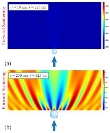
The previous section is devoted to the exact solution of light scattering problems for any sizes of spheres. The calculations of the scattered fields and cross sections can be formidable due to the complexity of the spherical Bessel functions. Moreover, the complex functions fail to reveal some intuitive insights of the light scattering behaviors under various conditions. Therefore, it is necessary to make reasonable approximations of the exact Mie theory in order to study the light scattering behaviors with different parameters such as particle sizes, scattering directions, wavelengths, refractive indices, as so on.
For particles much smaller than the wavelength (𝑎 ≪ 𝜆), it is possible to drop out the higher order terms of the power series expansions of the various spherical Bessel functions. For details, interested readers can refer to the books by Bohren and Kerker, where the original simple derivation by Lord Rayleigh is also described [64], [65]. Here I will directly go to the final expression for the scattering intensity under unpolarized illuminations as follows,
𝐼𝑠 =8𝜋
4𝑎6
𝜆4𝑟2 |
𝑚2− 1
𝑚2+ 2| 2
(1 + 𝑐𝑜𝑠2𝜃)𝐼 𝑖.
2.3 Light Scattering Intensity Distributions
Figure 2-5. (a) Rayleigh intensity pattern for single particle with 10 nm radius and 325 nm wavelength. (b) Mie scattering intensity pattern for 250 nm radius particle and 325 nm wavelength.
2.4 Summary
CHAPTER 3
COLLOIDAL PARTICLE SELF-ASSEMBLY TECHNIQUES
3.1 Molecular Self-Assembly
“Bottom-up” self-assemblies of molecules can provide resolutions that conventional “top-down” techniques could not achieve. There is much research effort in the techniques for assembling molecular scale objects, such as DNA and block copolymers. The DNA molecule has appealing features for use in nanofabrication because of its minuscule size with diameter of about 2 nanometers. In addition, the particularly powerful molecular recognition capability of the DNA molecules can be used to direct the assembly of highly complex nanostructures. 2D and 3D nanostructures with complex geometries and high resolutions have been demonstrated using branched DNA, DNA origami, and DNA bricks [67]–[70]. However, challenges still remain in the large-area fabrication of homogeneous assemblies of DNA.
3.2 Mechanism of Colloidal Particle Self-Assembly
Figure 3-1. Mechanism of colloidal particle self-assembly [77].
3.3 Ordered Particle Self-Assembly Techniques
Ordered particle assemblies can find many applications such as in photonic crystals [78], [79], and colloidal lithography for pattern transfer [54], [55]. Techniques to assemble ordered particle arrays are introduced in this subsection, including basic technique, such as drop casting, and advanced techniques, such as convective assembly by substrate withdrawal, self-assembly on air/water interface, and binary colloidal self-assembly.
3.3.1 Colloidal Self-Assembly by Drop Casting
assembly quality. In the assembly areas, monolayers are usually small, and large numbers of defects and multiple layers are present. This technique is useful when quick and small-scale demonstrations are required.
An even closer observation of the monolayers is shown in Figure 3-2(c), where representative grains and defects are labelled. It can be observed that the monolayers of nanoparticles are arranged in a hexagonal close-packed order, which is the minimum energy configuration. The assembly is polycrystalline with grain sizes in tens of micrometers and the grain boundaries are identified with orange lines. Defects are often present with nanoparticles assemblies, such as dislocations and point defects, due to the possible reasons of particle size distributions for monodispersed colloidal solutions, surface chemistry variations of substrates and lack of environmental parameter control.
Figure 3-2. Assembly of 750 nm diameter polystyrene nanospheres by drop casting on silicon substrate. (a) Photograph showing the assembled nanospheres. (b) Microscopic image of the assembled nanospheres with 50× magnification. (c) Microscopic image with 1000× magnification of
3.3.2 Colloidal Self-Assembly by Substrate Withdrawal
In drop casting, there is no environmental control during the self-assembly process and only limited areas of monolayers of 2D ordered colloidal crystals can be formed with simultaneous formations of multilayers. To scale up the fabrication of 2D uniform colloidal assemblies for useful applications, a substrate withdrawal technique was introduced by dragging a hydrophilic substrate vertically away from a colloidal suspension [80]. The mechanism of 2D colloidal crystal growth by substrate withdrawal is depicted in Figure 3-3, where the assembly consists of two stages, that is, the convective transfer of particles from bulk suspension layer and the assembly by capillary attraction in the drying region. For steady-state assembly, the following equation was proposed to describe the crystal growth [80],
𝑣𝑐 = 𝛽𝑗𝑒𝑙𝜑 ℎ(1 − 𝜀)(1 − 𝜑)
where vc is the colloidal crystal growth velocity, ε is the layer porosity, h is the height of the
assembled layer, φ is the volume fraction of the particle suspension, β is a coefficient that relates the solvent evaporation rate to the particle velocity (0 < β <1), and je is the evaporation
rate of pure water. From this equation, three major parameters can affect the colloidal crystal growth: (1) the substrate withdrawal velocity, vw, (2) the particle volume fraction, φ, and (3)
the solvent evaporation rate, je. For a steady crystal growth, the substrate withdrawal speed has
to be approximately equal to the colloidal crystal growth rate, vc ≈ vw. If the withdrawal velocity
convective flow can bring in excess particles to form thicker colloidal crystals with multilayers. Therefore, the substrate withdrawal speed has to match the colloidal crystal growth rate in order to achieve continuous uniform 2D colloidal crystal films. For higher particle concentrations, the colloidal film growth is faster. It was suggested that the humidity does not need to be controlled precisely to produce uniform coatings [81]. Therefore, the substrate withdrawal speed and the particle concentration play more important roles in the self-assembly process.
Direct substrate withdrawal from a bulk particle suspension can be inefficient in terms of time and material expense. Modified versions of the substrate withdrawal techniques, known as convective assembly, were introduced by confining a small volume of particle suspension in the gap between a substrate and a deposition plate [81], [82]. The deposition time and material expense are significantly reduced by higher suspension concentration and lower volume of the particle suspension. As shown in Figure 3-4, the deposition plate can be either angled or parallel to the substrate. These systems have been automated by digitally controlled motors for accurate speed control and have the potential to scale up for large-area assembly of colloidal crystals.
(a) (b)
Figure 3-4. Convective assembly techniques confine colloidal suspensions in (a) a wedge geometry [81] and (b) a parallel-plate geometry [82].
Figure 3-5. (a) Custom-built setup for self-assembly using substrate withdrawal. (b) Colloidal crystal films after self-assembly. (c) Optical microscope image of the colloidal crystal film using different
3.3.3 Colloidal Self-Assembly on Air/Water Interfaces
The techniques introduced so far are direct coating techniques for self-assembled colloidal monolayers on solid substrates. Additionally, there are indirect coating techniques which are based on the particle self-assembly on liquid/liquid or air/liquid interfaces and the subsequent transfer of the assembled layers to different substrates [83], [84]. This technique can also ensure the formation of large-area high-quality colloidal monolayers under proper conditions. It has been used for large-area demonstrations for high-quality, low-scattering optical films with near-unity refractive index and robust mechanical stability [85], as described in Chapter 6. This process is relatively simple, and does not require complex hardware and control systems. However, only hydrophilic surfaces can be coated with particle assemblies in this process because the assemblies happen on water surface and the substrate has to be hydrophilic to pick up any particle assemblies. Moreover, I have found that particles smaller than 350 nm diameter are difficult to form high-quality close-packed assemblies, and the reason might lie in the fact that more complex molecular interactions become pronounced for smaller particles.
close-packed monolayers. These monolayers can be picked up by either solid or soft substrates. Drying is needed after the transfer and at moderate evaporation speed, the monolayer order can remain unchanged. If fast evaporation takes place by heating or vacuum, film cracks can be observed and result in assembly defects. The experimental steps are also recorded in Figure 3-7(a)-(c) and the colloidal monolayers from 750 nm diameter polystyrene spheres are shown in Figure 3-7(d), where large grains were achieved and defects were still present. To achieve large-area low-defect colloidal monolayers, the self-assembly conditions have to be carefully controlled, such as the particle distributions on the spincoated substrate, PH value of the liquid phase, and the amount of the surfactant.
Figure 3-7. Self-assembly experiments using 750 nm diameter polystyrene nanospheres. (a) Immerse wafer with spincoated isolated nanospheres into water. (b) Add SDS to assemble nanospheres into ordered monolayers floating on the air/water interface. (c) Transfer the floating colloidal monolayers
3.3.4 Binary Colloidal Crystals
Figure 3-8. (a) Binary colloidal crystals from polystyrene nanospheres with (a) 500 nm and 220 nm diameters, and (b) 500 nm and 100 nm diameters. LS2 and LS3 crystal packings are observed.
3.3.5 Templated-Directed Self-Assembly
Figure 3-9. Template-directed self-assembly by substrate withdrawal. Polystyrene particles with 500 nm diameters are assembled on a positive photoresist substrate with micro-scale surface relief
topology [87].
3.4 Isolated Particle Assemblies with Random Order
Figure 3-10. Uniform isolated 750 nm diameter polystyrene nanoparticle assemblies with random order on a hydrophobic photoresist surface. (a) Optical image of the coated sample. (b) Dark field
optical microscope image of the colloidal particle assemblies.
3.5 Summary
CHAPTER 4
THREE-DIMENSIONAL NANOLITHOGRAPHY USING COLLOIDAL PARTICLES — NORMAL INCIDENCE
4.1 Fabrication Concept
Figure 4-1.Fabrication process of the hollow 3D nanostructures using light scattering from a colloidal nanoparticle. (a) FDTD simulation showing the scattering intensity pattern produced by TE-polarized UV light and a single nanosphere. Red and white indicate high and low intensities, respectively. (b)
4.2 Structure Modelling and Prediction
The FDTD software package, MEEP, was used to simulate the lithography system. Simulation was conducted in 3D with air and photoresist each occupying half the computation domain. The dielectric constants of polystyrene and photoresist are 2.79 and 3, respectively, and no absorption is considered. From the air medium, linearly polarized light with 325 nm wavelength illuminates a polystyrene sphere sitting on the air/photoresist interface at zero incident angle. Absorbing boundary conditions are applied on all the boundaries of the computation domain to mimic infinite media. Note that the horizontal dimensions of the computation domain perpendicular to the incident direction have to be large enough to avoid any influence of the absorbing boundary conditions on the particle light scattering pattern.
To study this patterning approach, I investigate the response of the materials to the light intensity distribution. The positive photoresist used in the experiments is modeled as a binary material, which becomes completely dissolvable in developer at a specific threshold dose. In addition, the photoresist material also absorbs UV light, so the intensity profile into the material is modulated by an exponential decay as described by Beer-Lambert law, given as,
𝐼 = 𝐼0𝑒−𝛼𝑙
where I0 is the incident intensity, α is the absorption coefficient, l is the length of the absorbing
ratios, this model can be validated by an iterative process of comparing the experimental results with different model parameters.
The colloidal light scattering can be described using the FDTD and the aforementioned binary resist models, and the nano-volcano geometries can be accurately predicted. Figure 4-2 illustrates a quantitative comparison of the patterned and predicted structures using a 1 μm diameter particle and 325 nm wavelength TE-polarized exposure (γ =3.08). The sidewall angles and thicknesses are compared, showing good agreement between the experiment and simulation. Note that the voids in the sidewall of the simulated cross section are enclosed spaces and cannot be dissolved by the developer in the experiments, forming a thick solid sidewall. These FDTD and binary resist models were used to predict all simulated nano-volcano structures in this work.
while (c) and (d) present a quantitative comparison of the same fabricated and simulated nano-volcano interiors, respectively.
Mie theory can also be used to predict the angular intensity profile of the scattered pattern but cannot accurately model the effect of multiple film layers, as shown in Figure 4-3. I examined the optical scattering using Mie theory, where the angular scattering field can be analytically derived. The intensity side lobes, which define the sidewall angles of the nano-volcanoes, can then be compared with the results using FDTD. A representative log-scale scattering field for γ = 1.84 in air is shown in Figure 4-3(a) for TE polarization. Model comparison is summarized for different particle diameter-wavelength ratios, as shown in Figure 4-3(b). The discrepancy between the two models stems from the far-field scattering field approximation and the complex multilayer photoresist/ARC/substrate stack, which Mie theory does not accurately predict. Given the relatively simple geometry and low computation costs, the solution from the FDTD is used for all predicted structures.
4.3 Single Nano-Volcanoes
Figure 4-4.Micrographs of the fabricated hollow 3D nanostructures using TE and TM-polarized 325 nm illuminations. The inset diagrams show the corresponding simulated nanostructures using FDTD method and a binary resist model. The nanostructures in each row were fabricated under the same conditions: (a)-(d) Particle diameter D = 450 nm, exposure dose = 130 mJ/cm2, γ = 1.38; (e)-(h) D = 750 nm, exposure dose = 120 mJ/cm2, γ = 2.30; (i)-(l) D = 1.9 µm, exposure dose = 130 mJ/cm2, γ =
5.85.
TE and TM illuminations. The angle in the TM plane is found to be larger than the angle in the TE plane because of the polarization effect. It can be observed that the sidewall angles are independent of doses, which in principle is expected because the scattering intensity pattern does not change with the exposure dose. For doses below 140 mJ/cm2, the experimental results agree with the simulations. However, the angles in the TE plane drop significantly at higher doses due to mechanical sagging of thinner sidewalls, which cannot be predicted by the optical model. The relationship of sidewall thickness versus dose is shown in Figure 4-6. The simulated and experimental results indicate decreasing sidewall thicknesses with increasing doses. The simulated sidewall for TM polarization is always thicker than that for TE polarization, which agrees with experiment. The thickness reduction results in a less mechanically stable nano-volcano structure, causing sagging of the sidewall at higher doses, which is observed previously in Figure 4-5. Figure 4-7 depicts the relationship of the top geometry with exposure dose, where a1, a2, w1, and w2 denote the long and short axes of the
Figure 4-5. Sidewall angle versus exposure dose from experimental data and FDTD simulations. The diagram shows the definition of the sidewall angle.
Figure 4-7. Top geometry feature sizes versus exposure dose from experimental data and FDTD simulations. The diagram shows the definition of the geometric parameters.
Figure 4-8. Operating shape diagram of the patterned 3D structures, showing the experimental results and FDTD simulations of the sidewall angle θ with respect to γ. Three regions of the achievable
hollow nano-volcano structures are presented in the diagrams. The dashed lines connecting the adjacent regions represent transitional regions, where shell damages are observed. The black dashed
lines are representative boundaries between regions, which are given by γ = 1.3 and 2.
direction. When the exposure light is unpolarized, the fabricated nano-volcanoes have cylindrical symmetry, as shown in Figure 4-9(b)-(d). These structures were fabricated using 500 nm diameter particles and an unpolarized mercury lamp narrow-band filtered at 365 nm. The value of γ is in region II of Figure 4-8, and an inner core can be observed in the nano-volcano, agreeing with the previous model. This result supports the conclusion that the phase diagram illustrated in Figure 4-8 is also applicable to unpolarized illuminations, which is expected given that the simulated TE and TM cases are similar. The shape of the particle can also affect the symmetry of the resultant nanostructures. If nonspherical colloidal elements are used, such as cubic particles or nanorods, the resultant structures are expected to resemble the symmetry of the elements and more complex geometries can be obtained.
Figure 4-9. Micrographs showing the polarization effect on the structural symmetry. (a) Top view of a nanostructure fabricated using a linearly polarized 325 nm laser and 500 nm diameter particles with exposure dose of 130 mJ/cm2 overlaid with the simulated structure. (b-d) Top, side and cross-section views of the nanostructures fabricated using an unpolarized mercury lamp narrow-band filtered at 365
4.4 Fabrication of Nano-Volcano Arrays
The hollow nano-volcano structures can also be patterned in a periodic array using light scattering from hexagonal non-close-packed particles, which allows precise spatial control of the surface structures. Since single nano-volcano is fabricated by light scattering from isolated particle, a nanosphere array that is not close-packed can produce periodic nano-volcano arrays. Figure 4-10 (a) and (b) depict the process to obtain such a periodic nanosphere mask. First, a monolayer of large polystyrene nanospheres is self-assembled into hexagonal close-packed array on the photoresist surface. The whole stack is then subjected to isotropic oxygen plasma etching, which reduces the particle diameter uniformly while preserving the periodic order. A thin layer of silicon dioxide was deposited on photoresist prior to particle coating to protect the photoresist during plasma etching. Subsequent UV light exposure and development processes produce the periodic nano-volcano arrays, as illustrated in Figure 4-10 (c) [92]. The plasma etching can preserve the spherical shape and the periodic order of the particles while reducing the particle diameter.
Figure 4-10. Fabrication process for periodic nano-volcano arrays. (a) An array of nanospheres is self-assembled on resist surface and is subjected to isotropic oxygen plasma etching to reduce the sphere diameter. (b) The whole stack is then exposed by UV light, resulting in (c) a periodic array of
The isotropic etching of the polymer colloids can be well controlled, as illustrated in Figure 4-11. In these experiments, samples with monolayers of close-packed 1 µm and 2 µm-diameter polystyrene particles were etched using a plasma Asher (PM-600, March Instruments). The etching parameters were 500 mTorr pressure, 250 W power and 80 sccm oxygen flow rate. For both cases, the etched particle volume, which is proportional to D3, has a linear relationship with the etching time after the etching process is stabilized. The insets in each graph show the evolution of the etching process, which preserves the spherical shape and the periodic order. The linear volume reduction relationship to time allows facile control of particle diameter, which in turn controls the geometry of resulting nano-volcano structures.
Figure 4-11. Characterizations of the isotropic etching processes of (a) 1 µm and (b) 2 µm-diameter nanospheres. After initial stabilization, the particle volume decreases linearly with etching time.
scattering from the neighboring particles can interfere with each other as depth approaches the period spacing. For the case in Figure 4-12(a) and (b), the strong interference starts from 700 nm depth. When the photoresist exceeds this thickness, the interference effect can damage the shell structure from bottom. For a high-quality nano-volcano array, the thickness of photoresist or the height of the nano-volcano array cannot exceed the limit defined by the separation between neighboring particles and the particle diameter-to-wavelength ratio.
Figure 4-12. FDTD simulations of the intensity pattern for 500 nm-diameter nanospheres in a 2 µm-period hexagonal array at orthogonal cross sections. Interference between scattering patterns occurs beyond 700 nm thickness. Simulated nano-volcano arrays are for depths of (c) 500 and (d) 700 nm,
respectively.
thickness of the photoresist to 500 nm, the same 2 μm period array can have improved structural quality, as shown in Figure 4-13(c). The thickness of photoresist should be chosen within the height limit to avoid light interference between neighboring particles, which depends on the particle array period and the particle diameter-to-wavelength ratio. The dependency of these factors on structure control is currently under investigation.
Figure 4-13. Micrographs of the periodic nano-volcano arrays with (a) 1 μm period and 1 μm height, (b) 2 μm period and 1 μm height, (c) 2 μm period and 500 nm height.
4.5 Application as Drug Delivery Surfaces
can be transferred to the releasing medium, such as a water environment. The release can be passive in nature by pure material diffusion until fully depleted. More interestingly, one can actively trigger the release using a phase change material (PCM) as the loading medium for molecules and nanomaterials by changing the temperature. The temperature change can be realized by different methods such as light radiation, ultrasonic agitation, and plasmonic local heating. The end product will be a drug delivery transdermal patch with loaded nano-volcano arrays and programmable delivery dosage and schedule.
Figure 4-14. Nano-volcano drug delivery concept.
Figure 4-15. Micrographs of particle-trapping nano-volcanoes. The 50 nm diameter silica particles are trapped in (a) double-shelled and (b) thick-walled nano-volcanoes.
several seconds of oxygen plasma treatment, which can prevent 1-tetradecanol from adhering to the surface for easy removal of the excess materials after loading. The removal process of 1-tetradecanol is depicted in details in Figure 4-16. A beaker of hot water is covered with a pond of 1-tetradecanol above the melting point and the loaded nano-volcano samples will have excess amount of 1-tetradecanol on the whole sample surface, as shown in Figure 4-16(a). The nano-volcano sample is then moved vertically through the 1-tetradecanol pond into water. The water molecules ‘like’ to adhere to the plasma-treated sample surface because of hydrophilicity to break the attachment of excess tetradecanol, and the surface tension between water and 1-tetradecanol helps the removal of 1-1-tetradecanol from the sample surface, as shown in Figure 4-16(b). The sample may be recovered when water cools down and 1-tetradecanol becomes solid. During the whole removal process, the loaded particles are free to diffuse out of the nano-volcanoes, and an improved method may be needed.
Figure 4-17. Fluorescent particle loading. (a) Confocal microscope image of nano-volcanoes loaded with PCM and fluorescent particles. (b-c) Scanning electron microscope images of loaded
nano-volcanoes.
The simulation was conducted in MEEP and the analysis method was adapted from online examples for silver particles in air [94]. For lithography, the metal particle has to sit on a photoresist surface, which is not easily modelled by Mie theory as shown previously. Details about the simulation setup can be found in the online example. The calculation of extinction efficiencies, which is the sum of absorption and scattering efficiencies, has to take into account the existence of photoresist. Therefore, three sets of simulations has to be performed. The first set of simulation will be calculating the incident light intensity, I0, with only air as medium.
The second set will be used to calculate the absorption efficiency with metal particle and photoresist. Six surface monitors forming a closed cube surrounding the metal particle are set to record the total transmitted light power, Pabs. The last set of simulations will calculate the
scattering efficiency with the presence of metal particle and photoresist excluding the transmitted light power without the metal particle through the same closed surface monitors in the absorption simulations. The total transmitted light power surrounding the particle is the scattering light power, Pscat. The physical cross section of the metal particle is S. Then the scattering, absorption, and extinction efficiencies are calculated using the following relationships,
𝛼𝑠𝑐𝑎𝑡 =
𝑃𝑠𝑐𝑎𝑡 𝐼0𝑆
, 𝛼𝑎𝑏𝑠 =
𝑃𝑎𝑏𝑠 𝐼0𝑆
𝛼𝑒𝑥𝑡 = 𝛼𝑠𝑐𝑎𝑡+ 𝛼𝑎𝑏𝑠
where αext, αscat, and αabs are extinction, scattering and absorption efficiencies.
Figure 4-18. (a) Scattering characteristics of 50 nm-diameter silver nanoparticle on photoresist. Two resonances are observed at 353 nm and 399 nm. (b-c) Top view and cross-sectional view of quadrupole resonance at 353 nm wavelength using logarithmic plot with base of 10. (d-e) Top view and cross-sectional view of dipole resonance at 399 nm wavelength using logarithmic plot with base
4.7 Summary
CHAPTER 5
THREE-DIMENSIONAL NANOLITHOGRAPHY USING COLLOIDAL PARTICLES — OBLIQUE INCIDENCE
In the previous chapter, the colloidal particles are subjected to normal incidence to generate upright ‘nano-volcanoes.’ However, due to the existence of an air-photoresist interface, the scattering pattern can vary under different incident angles. In this chapter, I will explore the extended fabrication capabilities of the 3D nanolithography described in the previous chapter by simply tilting the illumination. This simple modification also allows us to introduce more controllable lithography parameters to fabricate a large variety of 3D nanostructures.
electron-beam/focused-ion beam [33], interference/holographic [38], and multi-photon lithography [36], [37], [95]. Since the scattering mechanisms do not rely on coherence, lasers are not required and any narrowband light source can be used. Harnessing the particle-light interactions also enable novel local scattering patterns, and expands on the use of colloidal elements beyond self-assembly systems. The particles are assembled directly on the photoresist surface, ensuring intimate contact between the colloidal particles and the photoresist. Isolated colloidal particles are the focus of this work, but the proposed method can also be applied to multiple particles, non-spherical colloids and their assemblies to fabricate exotic nanostructures [52], [53]. Plasmonic interaction described in the previous chapter is also possible using metal particles to fabricate subwavelength surface features.
5.1 Fabrication Concept
![Figure 1-1. (a) Antireflective nanostructures of moth eye [1]. (b) Directional dry adhesive](https://thumb-us.123doks.com/thumbv2/123dok_us/1472802.1180376/22.612.135.495.299.603/figure-antireflective-nanostructures-moth-eye-directional-dry-adhesive.webp)
![Figure 1-2. Multifunctional glass [13]. (a) Nanocone structures. (b) Multifunctionalities of nanocone structures](https://thumb-us.123doks.com/thumbv2/123dok_us/1472802.1180376/23.612.191.439.325.625/figure-multifunctional-glass-nanocone-structures-multifunctionalities-nanocone-structures.webp)
![Figure 1-7. Phase-shift lithography process [42].](https://thumb-us.123doks.com/thumbv2/123dok_us/1472802.1180376/31.612.105.524.302.617/figure-phase-shift-lithography-process.webp)
![Figure 1-8. 3D nanostructures by colloidal particle self-assembly [45].](https://thumb-us.123doks.com/thumbv2/123dok_us/1472802.1180376/33.612.160.472.69.329/figure-d-nanostructures-colloidal-particle-self-assembly.webp)
![Figure 1-9. Colloidal lithography using colloidal particle assemblies as deposition masks [54], [55]](https://thumb-us.123doks.com/thumbv2/123dok_us/1472802.1180376/35.612.118.509.136.388/figure-colloidal-lithography-using-colloidal-particle-assemblies-deposition.webp)
![Figure 1-10. Three-dimensional nanolithography using colloidal particle phase masks [60]](https://thumb-us.123doks.com/thumbv2/123dok_us/1472802.1180376/36.612.148.483.168.615/figure-dimensional-nanolithography-using-colloidal-particle-phase-masks.webp)
![Figure 2-2. Interpretation of scattering mechanism [65].](https://thumb-us.123doks.com/thumbv2/123dok_us/1472802.1180376/42.612.139.503.85.351/figure-interpretation-of-scattering-mechanism.webp)
![Figure 2-4. Field lines of total Poynting vector excluding scattered light near a small Al sphere [66]](https://thumb-us.123doks.com/thumbv2/123dok_us/1472802.1180376/51.612.232.400.432.656/figure-field-lines-poynting-vector-excluding-scattered-sphere.webp)