Analysis and Design of Hybrid 4 bit CLA
Full Adder
Iti Sharma, Shiraz Husain
Dept. of Electronics and Communication, Shri Vaishnav Institute of Technology and Science, Indore, M.P. India
Assistant Professor, Dept. of Electronics and Communication Engineering, Shri Vaishnav Institute of Technology and
Science, Indore, M.P. India
ABSTRACT: The paper presents implementation and analysis of benchmark circuit ISCAS 74283at 32nm technology. Study of various logic style is done and ultimately a hybrid ISCAS 74283 is developed by performing gate replacement. The adder utilizes 5 input GDI based NOR gate as a hybrid part. Proposed circuit is hybrid as it utilizes CMOS conventional logic style as well as GDI logic style. At the end of the work it is observed that replacement of CMOS gate with GDI gate improves performance and power dissipation of overall 74283. Comparative power product delay analysis is presented in conclusion.
KEYWORDS: CLA, Full Adder, ISCAS 85 74283, static power, GDI logic, gate replacement.
I. INTRODUCTION
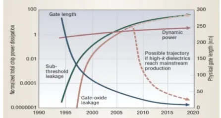
Historically, when first transistors were evolved, there were technologies based on BJT, NMOS to design integrated circuits. With evolution of CMOS technology it was realized that power consumption reduced considerably as static power dissipation of CMOS circuits is ideally zero reason being that there is never a complete path between Vdd and ground. But later as the technology shrink down it was realized that scaling down the technology i.e. transistor size leads to leakage in transistor and this leaky transistor completes the rail between Vdd and ground. The ITRS report projects a decrease in dynamic power per device over time due to scaling of Vdd [1] [2]. However, if we assume a doubling of on-chip devices every two years, total dynamic power will increase on a per-chip basis. Packaging and cooling costs as well as the limited power capacity of batteries make this trend unsustainable. In it is reported that sub-threshold leakage power dissipation of a chip may exceed dynamic power dissipation at the 65nm feature size as shown infig1 [2].
The significant interest is in power reduction because of two reasons. Firstly it is associated with cooling consideration of high performance circuits. Excess heat due to power dissipation must be removed from the system on which circuit is mounted. Secondly it is associated with portability of device. With goal of low consumption circuit development above listed two demands can be definitely fulfilled.
Power minimization techniques can be applied at various levels. Among all the design level which researcher opt to work, one that get most attention to mitigate power is circuit level. Because circuit level analysis has significant potential for power saving [3].
Selecting appropriate logic style to implement circuit can minimize power to considerable amount and apart from this logic style can significantly influence speed, complexity and size of circuit to be implemented. Logic style affect speed as delay of circuit basically depend on the number of inversion levels in circuit, number of stacks in implementation of logic and cell wiring.
To meet requirement some logic style such as Gate diffusion input- GDI is developed that are as easy as CMOS to implement and at the same time can take care of power and performance in deep submicron region
II. RELATED WORK
In [2] authors used average residual battery level of the entire network and it was calculated by adding two fields to the RREQ packet header of a on-demand routing algorithm i) average residual battery energy of the nodes on the path ii) number of hops that the RREQ packet has passed through.According to their equation retransmission time is proportional to residual battery energy. Those nodes having more battery energy than the average energy will be selected because its retransmission time will be less. Small hop count is selected at the stage when most of the nodes have same retransmission time. Individual battery power of a node is considered as a metric to prolong the network lifetime in [3]. Authors used an optimization function which considers nature of the packet, size of the packet and distance between the nodes, number of hops and transmission time are also considered for optimization. In [ 4] initial population for Genetic Algorithm has been computed from the multicast group which has a set of paths from source to destination and the calculated lifetime of each path. Lifetime of the path is used as a fitness function. Fitness function will select the highest chromosomes which is having highest lifetime. Cross over and mutation operators are used to enhance the selection. In [5] authors improved AODV protocol by implementing a balanced energy consumption idea into route discovery process. RREQ message will be forwarded when the nodes have sufficient amount of energy to transmit the message otherwise message will be dropped. This condition will be checked with threshold value which is dynamically changing. It allows a node with over used battery to refuse to route the traffic in order to prolong the network life. In [6] Authors had modified the route table of AODV adding power factor field. Only active nodes can take part in rout selection and remaining nodes can be idle. The lifetime of a node is calculated and transmitted along with Hello packets. In [7] authors considered the individual battery power of the node and number of hops, as the large number of hops will help in reducing the range of the transmission power. Route discovery has been done in the same way as being done in on-demand routing algorithms. After packet has been reached to the destination, destination will
wait for time δt and collects all the packets. After time δt it calls the optimization function to select the path and send
RREP. Optimization function uses the individual node’s battery energy; if node is having low energy level then optimization function will not use that node.
III.PROPOSED ALGORITHM
A. ANALYSIS OF CLA:
Circuit carry look ahead adder is a bench mark circuit for international symposium on circuits and system-ISCAS under 74X-Series Circuits listed as 74283 circuit. ISCAS was first started in 1968 by theorist of IEEE. ISCAS circuits are used by researcher as basis for comparing results.
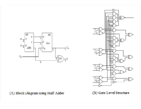
73283 listed as ISCAS circuit is fast adder circuit with 9 inputs 5 outputs and 36 gates.[4]
Fig. 2. benchmark circuit ISCAS 74283
As already mentioned earlier CLA work on generation and propagation of carry. Generated and propagated carry are given by Gi and Pi.
= ∗ ... 1
= ⨁ ... 2
By the above equations Ci at various positions can be calculated by equation 9 and finally when all the carries are known it takes very small time to compute sum. Sum is calculated using equation 10
= + ... 3
= ⨁ ... Error! Bookmark not defined.
B. LOGIC STYLES:
In order to make a logic style simple and for its ease-of-use, the logic style should be designed in such a way that it is highly vigorous and have approachable and generalized electrical characteristics that is it should have good driving capabilities and should offer full signal swing at output. This feature allow logic gate cascading and hence reliability of combinational circuits and are prerequisite for logic synthesis and base design of cell. Logic style must provide regularity for the implementation of random logic design and should allow efficient implementation [4]
Conventional CMOS logic
In CMOS also referred as conventional or complementary logic gates are built from pull up and pull down network, pull
capability. However, this weak output driving or swing problem can be corrected by using buffers/inverters at output. In CMOS logic style the transistor networks consist only of a series of up to three transistors between power lines and gate output, thus eliminating the usage of pass-gates. The transistor branch offers higher layout regularity and simple characterization.
Gate Diffusion Input
GDI method is based on a simple cell of two transistor shown in fig. 3 it has three inputs those are G- common gate input, P- input to source/drain of PMOS, N- input to source/drain of NMOS. GDI logic is very significant compared to other logic styles because it allow improvement as transistor count is reduced and also there is improvement in design complexity as compared to other logic styles. GDI logic style is advantageous over conventional CMOS logic because it can be considered as the extended version of CMOS logic as in GDI each cell has 2 more inputs i.e. number of transistor in n input CMOS is equal to n+2 input GDI cell transistor.[8]
Fig. 3. Basic GDI cell [9]
Implementation of GDI can be done by using following expression, by implementing logic using this expression three input CMOS structure can be converted to five input GDI structure. GDI approach is a combination of Shannon expansion and combinational logic precomputation.
= ( … … ) + ( … … ) 4
For implementing a function using GDI firstly minimize the expression and check if it is not equal to 1,0 or any inverted single variable. If it is equal no hardware implementation is needed else Shannon expression is used for given function. GDI cell will be implemented using product of Shannon expansion H, G and X1. Further function H and G will be treated as function and implemented using Shannon expansion. [6]
( … = (1, … ) + (0, … ) 5
IV.DESIGNINGHYBRIDCIRCUITBYGATEREPLACEMENT
The base design was designed using CMOS transistors and problem is theoretically proven and experimentally analyzed that power is increasing with scaling when using CMOS logic implementation of circuits.
In [5][6][7] two input basic gate has been proposed. Generally replacement of universal gates i.e. NAND gate and NOR gate developed using CMOS logic with GDI logic universal gate is avoided because the number of transistor count in both logics is same and the advantages of GDI logic are not reflected in universal gates. Power of universal gates using GDI logic is more because the stacking in CMOS is more compared to GDI for universal gate and at the same time improper output swing is incorporated in GDI logic.
In this work 5 input NOR GATE is replaced because studies of gate at various inputs reveals that power dissipated in proposed gate network is lesser than that of CMOS logic gate.
Modified gate structures
In this work 5 input NOR GATE is designed using Shannon expansion theorem, which is the basis for development of GDI logic.
F= + + + + 6
= ( + + + + ) + ( + + + + ) ̅
= ( + + + ) + ( + + + )
= ( + ) + ( + ) = ( ) + ( )
Can be implemented as
Fig. 4. Basic cell of ladder 5 input NOR
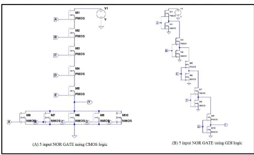
Fig.5. shows the 5 input NOR gate using CMOS logic and gate i.e. replacing it. It is clear that CMOS gate have 5 PMOS transistors stacked so it dissipates least power when all the PMOSes are off because stacking is introduced in circuit but at the same time for some of input vectors power dissipated is 10 times of that of average power. The proposed network on the other hand is a repetitive ladder type network thus even the worst case don’t increase power to multiple folds.
Fig. 5. 5 input NOR gate implementation
Hybrid ISCAS 74283
Fig. 6. Replacement of 5 input NOR in ISCAS 74283
Fig. 6 shows that the 5 input NOR gate is been replaced by proposed gate resulting in a hybrid ISCAS 74283 circuit. And this replacement is done because when analysed separately the overall power of 5 input NOR gate is reduced 1.4X to that of conventional 5 input NOR gate.
V. SIMULATION RESULTS
All the above methods are applied on ISCAS 85 74283 and net list for the circuit is written and simulated using HSPICE simulator. Various parameters and their impact on circuit designs are studied. The analysis is done at 1V,Vdd and 270C.
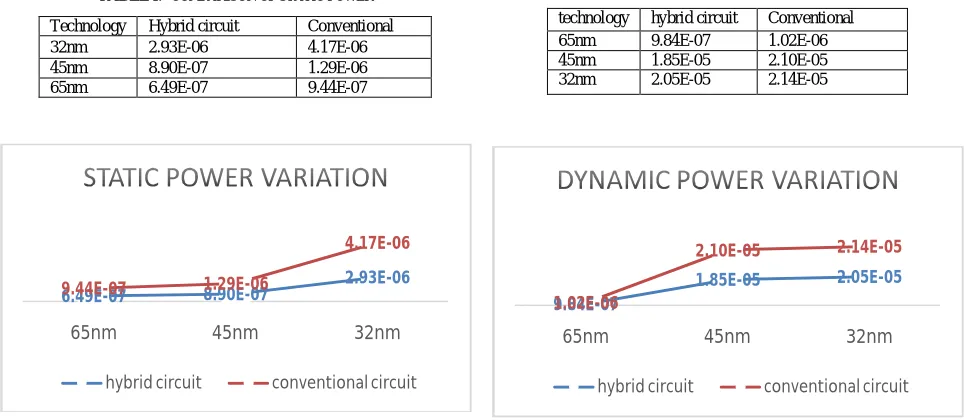
TABLE I. COMPARISON OF STATIC POWER
Technology Hybrid circuit Conventional
32nm 2.93E-06 4.17E-06
45nm 8.90E-07 1.29E-06
65nm 6.49E-07 9.44E-07
Fig. 7. Comparison of static power
TABLE II. COMPARISON OF DYNAMIC POWER
technology hybrid circuit Conventional
65nm 9.84E-07 1.02E-06
45nm 1.85E-05 2.10E-05
32nm 2.05E-05 2.14E-05
Fig. 8. Comparison of dynamic power
6.49E-07 8.90E-07 2.93E-06
9.44E-07 1.29E-06
4.17E-06
65nm 45nm 32nm
hybrid circuit conventional circuit
9.84E-07
1.85E-05 2.05E-05
1.02E-06
2.10E-05 2.14E-05
65nm 45nm 32nm
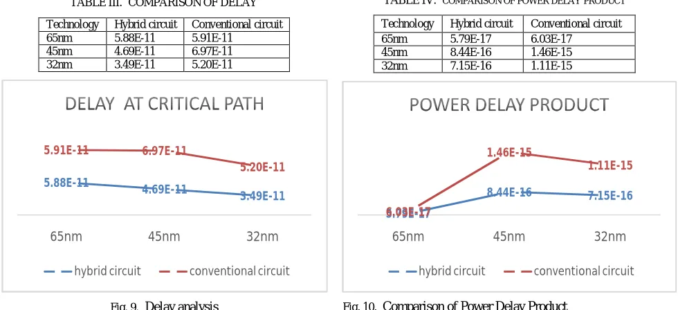
TABLE III. COMPARISON OF DELAY
Technology Hybrid circuit Conventional circuit
65nm 5.88E-11 5.91E-11
45nm 4.69E-11 6.97E-11
32nm 3.49E-11 5.20E-11
Fig. 9. Delay analysis
TABLE IV. COMPARISON OF POWER DELAY PRODUCT
Technology Hybrid circuit Conventional circuit
65nm 5.79E-17 6.03E-17
45nm 8.44E-16 1.46E-15
32nm 7.15E-16 1.11E-15
Fig. 10. Comparison of Power Delay Product
The benchmark circuit is simulated at 65nm, 45nm and 32nm and the proposed circuit is compatible for all the mentioned technologies that is shows same effect on power, delay and power delay product at each technology. Replacement of single NOR gate in the circuit shows 3% static power reduction at selected set (set of 32 random inputs). When simulated for the worst case input for critical path power is minimized 23.4%, at the same time critical path delay is also minimized by 38.1% and 56.85% improvement is seen in PDP that is power delay product.
VI.CONCLUSION AND FUTURE WORK
Adder is one of the most important unit to perform arithmetic operation and is a part of all processors. In this work a low power and high performance hybrid 4 bit CLA is developed. This hybrid CLA consist of conventional CMOS logic style as well as GDI logic style. In first phase of work the prior methods to minimize power have been applied to the benchmark circuit selected to carry this work. But each of the method have certain disadvantages of its own in terms of area, delay or complexity of design and operation. Where as in this work a single 5 input NOR gate is proposed and placed in circuit in place of conventional 5 input NOR gate. In the proposed circuit of gate the transistor count of 5 input NOR gate is same as that of conventional CMOS 5 input NOR gate and also improper output swing which is problem with most of the logic technique is not observed for proposed gate. And the architecture is also a symmetric and easily implementable.
In future the other gates in the combinational circuit can also be designed to further minimize the power. Also the advantage of two methods can be incorporated to minimize power that is applying prior power mitigating methods can be applied to hybrid circuit to further improve performance along with a balance with power
REFERENCES
[1] kausik roy, saibal mukhopadhyay hamid mahmoodi- meimand, "leakage current mechanism and leakage reduction techniques in deep submicrometer CMOS circuits," proceedings of IEEE, vol. 91, february 2003.
[2] "International Technology Roadmap for Semiconductors,," Semiconductor Industry Assoc., 2013. [Online]. Available: http://public.itrs.net. [3] "semiconductor manufacturing and design," aprill 2016. [Online]. Available: http://semimd.com/blog/tag/moores-law/.
[4] Nam Sung Kim, Todd Austin, David Blaauv and Trevor Mudge, Leakage Current: Moore's Law Meets Static Power, IEEE Computer Society, December 2003.
[5] W. Linda, "More than Moore, White Paper," Semiconductor Industry Association, Update 2012. [Online]. Available: http://www.itrs.net/Links/2010ITRS/IRC-ITRS-MtM-v2%203.pdf.
[6] M. Hansen, H. Yalcin, and J. P. Hayes,, "Unveiling the ISCAS-85 Benchmarks: A Case Study in Reverse Engineering,," IEEE Design and Test,, Vols. 16, no. 3, pp. 72-80, July-Sept 1999.
5.88E-11
4.69E-11 3.49E-11
5.91E-11 6.97E-11
5.20E-11
65nm 45nm 32nm
hybrid circuit conventional circuit
5.79E-17
8.44E-16 7.15E-16
6.03E-17
1.46E-15
1.11E-15
65nm 45nm 32nm
[7] Ajay Kumar Singh, "Combinational Static Logic Circuit," in Digital VLSI Design, New Delhi , PHI Learning Pvt. Ltd., 2010, pp. 193-230. [8] Arkadiy Morgenshtein, Alexander Fish and Israel A. Wagner, "Gate Diffusion Input GDI- A Power Efficient Method for Digital Combinational Circuits," IEEE transection on very large scale integration system, vol. 10, no. 5, pp. 566-581, october 2002.
[9] Arkadiy Morgenshtein, Alexander Fish and Israel A. Wagner, "Gate Diffusion Input(GDI)- A Technique for Low Power Design of Digital Circuit: Analysis and Characterization," IEEE, pp. 477-480, 2002.
[10] Pankaj Verma , Ruchi Singh and Y. K. Mishra, "Modified GDI Technique- A Power Efficient Method for Digital Circuit Design," International Journal of Advanced Technology in Engineering and Science, vol. 01, no. 10, pp. 17-39, october 2013.
![Fig. 3. Basic GDI cell [9]](https://thumb-us.123doks.com/thumbv2/123dok_us/1425661.1175075/4.595.235.377.300.439/fig-basic-gdi-cell.webp)