ABSTRACT
REITMEIER, ZACHARY JUSTIN. The Chemistry and Surface Microstructure of Si-Based Substrates and their Effect on the Evolution of the Microstructures of III-Nitride Films Grown via Metalorganic Vapor Phase Epitaxy. (Under the direction of Dr. Robert F. Davis)
cathodoluminescence for GaN layers on stripe-patterned Si substrates. However, long growth times resulted in outdiffusion of Si from the substrate and subsequent film
T
HEC
HEMISTRY ANDS
URFACEM
ICROSTRUCTURE OFSi-B
ASEDS
UBSTRATESAND THEIR
E
FFECT ON THEE
VOLUTION OF THEM
ICROSTRUCTURES OFIII-N
ITRIDEF
ILMSG
ROWN VIAM
ETALORGANICV
APORP
HASEE
PITAXYby
Zachary J. Reitmeier
A dissertation submitted to the Graduate Faculty of North Carolina State University
In partial fulfillment of the Requirements for the degree of
Doctor of Philosophy In
Materials Science and Engineering Raleigh, NC
2005 Approved by:
___________________________ ___________________________
Dr. Robert F. Davis Dr. Zlatko Sitar Chair of Advisory Committee
___________________________ ___________________________
DEDICATION
For Lisa
At times our own light goes out and is rekindled by a spark from another person. Each of us has cause to think with deep
iii
BIOGRAPHY
ACKNOWLEDGMENTS
The contents of this dissertation would not have been possible without the help and support of numerous people. On the professional side, I would like to express my gratitude to my advisor Dr. Robert Davis for providing me with this opportunity and teaching me so much about the field of materials science as well as research techniques and practices in general. I also had the benefit of working with and learning from Drs. Sven Einfeldt, Pete Miraglia, Ed Preble and Amy Roskowski, each of whom taught me an incredible amount during my time at NCSU. The time I spent with each of them was invaluable. Thanks are also extended to my committee members Drs. Zlatko Sitar, Mark Johnson, and John Muth for their assistance and participation in my research as well as to other members of the Davis group including Ji-Soo Park, Seann Bishop, and Will Mecouch for their help over the last several years. Additionally, thanks go out to Yoga Saripalli for assistance with the cathodoluminescence measurements, Dr. Jeffrey Eischen for assistance with the finite element calculations, and to Jan Jackson and Edna Deas for help on too many issues to list here. I also had the benefit of working with numerous collaborators outside of NCSU. In particular, I would like to thank Dr. Subhash Mahajan at Arizona State University and Dr. Roland Kröger at the University of Bremen for their contributions to this work.
On the personal side, I would first like to thank my parents, Skip and Ellin, for their constant support and encouragement throughout my life and for instilling in me a sense of hard work and a belief in the importance of education. If I am half the parent that they are, I will consider myself a success.
v
TABLE OF CONTENTS
Page
List of tables ix
List of figures x
1. Introduction 1
1.1 References 8
2. Surface and defect microstructure of GaN and AlN on 6H-SiC(0001)
substrates 11
2.1 Abstract 12
2.2 Introduction 13
2.3 Experimental procedure 15
2.4 Results and discussion 17
2.4.1 Surface microstructures and growth modes of AlN on SiC substrates 17 2.4.2 Defect microstructure of AlN on SiC substrates 18 2.4.3 Surface microstructures and growth modes of GaN on AlN/SiC
substrates 20
2.4.4 Defect microstructure of GaN on AlN/SiC substrates 22
2.5 Summary 25
2.6 References 27
2.7 Figures 31
3. Surface morphology and strain of GaN layers grown using 6H-SiC(0001)
substrates with different buffer layers 40
3.1 Abstract 41
3.2 Introduction 41
3.3 Experimental procedure 42
3.4 Results and discussion 43
3.4.1 Surface morphology 43
3.4.2 Strain 47
3.5 Summary 51
3.6 References 52
4. On the microstructure of AlxGa1-xN layers grown on 6H-SiC(0001) substrates 54
4.1 Abstract 55
4.2 Introduction 55
4.3 Experimental details 56
4.4 Experimental results 58
4.5 Discussion 64
4.6 Summary 68
4.7 References 69
4.8 Figures 71
5. Surface and defect microstructure of GaN and AlN on hydrogen-etched
6H-SiC(0001) substrates 83
5.1 Abstract 84
vii
5.4 Results and discussion 91
5.4.1 Surface microstructure and growth mode of AlN on HE-SiC 91 5.4.2 Defect microstructure of AlN on HE-SiC 94 5.4.3 Surface microstructure and growth mode of GaN on AlN/HE-SiC 95 5.4.4 High resolution X-ray diffraction 97 5.4.5 Defect microstructure of GaN on AlN/HE-SiC 101
5.5 Summary 101
5.6 References 104
5.7 Tables and figures 109
6. Cantilever epitaxy of GaN on Si(111) substrates as a route towards
freestanding pseudo-bulk GaN substrates 120
6.1 Abstract 121
6.2 Introduction 122
6.3 Models of stress and strain in cantilever epitaxy on silicon 126
6.3.1 Mechanics model 127
6.3.2 Finite element model 132
6.4 Experimental procedure 134
6.4.1 Silicon processing and III-Nitride growth 134
6.4.2 Characterization 135
6.5 Results and discussion 136
6.5.1 Growth rate and morphology of GaN as a function of growth conditions
and Si stripe geometry 136
6.5.2 Characterization of cantilever epitaxy-grown GaN 146 6.5.2.1 High resolution X-ray diffraction 146
6.5.2.2 Cathodoluminescence 148
6.5.2.3 Transmission electron microscopy 152 6.5.3 Growth instability due to silicon outdiffusion 156 6.5.4 Thick GaN layers deposited by HVPE on cantilever GaN templates 164
6.6 Summary 165
6.7 References 169
6.8 Tables and figures 179
7. In-situ cleaning of GaN(0001) surfaces in an MOVPE environment 204
7.1 Abstract 205
7.2 Introduction 206
7.3 Experimental procedure 207
7.4 Results and discussion 208
7.4.1 Profiles of impurity concentrations 208 7.4.2 AFM of homoepitaxial GaN films 210 7.4.3 SEM and AFM of GaN templates 211
7.5 Summary 215
7.6 References 216
7.7 Tables and figures 218
8. Summary of the dissertation 225
Appendix 1 Growth and Characterization of AlN and GaN Thin Films
A1.1 Abstract 232
A1.2 Introduction 232
A1.3 Experimental procedure 234
A1.4 Results and discussion 235
A1.5 Summary 238
A1.6 References 239
ix
LIST OF TABLES
Page
Chapter 3
Table I Growth conditions used for the AlN buffer layer, the AlGaN buffer layer, and the GaN epilayer, respectively.
43 Table II Measured lattice parameters, ao and co, for 4 µm thick GaN layers
grown on AlN and AlGaN buffer layers, respectively. The numbers given for -2c13/c33, to, and ∆εxx are results of fitting Eqs.(2) and (3) to
the experimental data shown in Fig. 7.
49
Chapter 5
Table I Measured lattice parameters, ao and co, and in-plane and out-of-plane
strain, εxxand εzz respectively, for 1 µm thick GaN films deposited on
100 nm AlN buffer layers on as-received and hydrogen-etched 6H-SiC(0001) substrates. Stains are calculated based on the lattice parameters for undoped homoepitaxial GaN given in [51]. Negative strain values indicate compression and positive values indicate tension.
109
Chapter 6
Table I Input parameters for the finite element model of the cantilever GaN/Si structure.
179
Chapter 7
Table I Annealing conditions for GaN/AlN/SiC templates heated to 1020°C in an MOVPE system. N2/H2 refers to an ambient composed of 4 slm N2
+ 3 slm H2. NH3/H2 refers to an ambient composed of 4 slm NH3 + 3
slm H2.
LIST OF FIGURES
Page
Chapter 2
Figure 1 10x10 µm and 2x2 µm AFM height images of mechanically polished 6H-SiC(0001) substrates ((a) and (d), respectively) and AlN(0001) layers ((b) and (c) and (e) and (f), respectively) grown on the 6H-SiC. The layer thickness is noted in the upper left corner of each image, and the vertical height scale is given on the upper right. A polishing scratch into which AlN islands have grown is indicated by the arrows in Fig. (f).
31
Figure 2 Cross-sectional TEM image of a 15 nm A1N/as-polished SiC substrate composite. The operating reflection is (0002) for which all a type dislocations should be out of contrast. Note the presence of strains in both the layer and the substrate.
32
Figure 3 Plan-view TEM micrograph obtained from a 15 nm A1N/as-received SiC substrate composite. Steps delineated by misfit dislocations are visible and networks of misfit dislocations on terraces are complex.
33
Figure 4 (a) Schematic showing a hexagonal network of misfit dislocations on a terrace; one segment is aligned along a step; (b) Schematic showing hexagonal dislocation networks on two terraces; segments of misfit dislocations tend to align with step edges.
34
Figure 5 (a) – (i) 2x2 µm AFM height images of GaN layers grown on 100 nm AlN buffer layers. The layer thickness is based on established growth conditions and is listed in the upper left corner of each image. The vertical height scale is given in the upper right corner of each image. Note the GaN islands observed in (b) and (c) and the step terminations indicated by arrows in (h) and (i). The lower right inset in (d) shows a single 2 µm long scan line which allows the observation of the flat-topped nature of the GaN islands. The vertical height range of this inset is 8 nm.
35
Figure 6 (a) – (c) 10x10 µm AFM height images of GaN layers grown on 100 nm AlN buffer layers. The layer thickness is based on established growth conditions and is listed in the upper left corner of each image. The vertical height scale of each image is given in the upper right corner of each image. The layers are the same samples as those labeled with the same nominal thicknesses in figure 2. Note the influence of the undulations in the AlN buffer layer on the nucleation of the GaN islands.
36
Figure 7 Cross-sectional TEM WBDF images from a 1000 nm GaN/15 nm A1N/as-polished SiC substrate composite: (a) operating reflection is
) 00 1 1
( , (b) enlargement of a region marked by an arrow in (a), and (c) operating reflection is (0002).
xi
Figure 8 Cross-sectional TEM WBDF images from a 2000nm GaN/100 nm A1N/as-deposited SiC substrate composite: (a) operating reflection is
) 110 2
( , and (b) operating reflection is (0002).
38
Figure 9 Plan-view image from a 2000 nm GaN/100 A1N/as-polished SiC substrate composite. Note that TDs appear to form a mosaic structure.
39
Chapter 3
Figure 1 2 µm x 2 µm AFM surface images of GaN layers grown at 1010°C on AlN buffer layers. The GaN layer thickness is indicated for each image. Note the GaN islands marked by arrows in micrographs (c) and (d).
44
Figure 2 Height versus diameter of GaN islands grown on an AlN buffer layer (circles). The data was extracted from AFM images of GaN layers with nominal thicknesses of 1.5 and 2 nm, respectively. The aspect ratios of 1/60 and 1/20 are marked by dotted and dashed lines, respectively.
45
Figure 3 2 µm x 2 µm AFM surface images of GaN layers grown on AlGaN buffer layers. The GaN thickness is indicated for each image. Note the spiral hillock in (a) and the very narrow, irregularly curved trenches marked by arrows in micrograph (a).
45
Figure 4 Peak-to-valley surface roughness of GaN layers of different thickness grown on AlN buffer layers (filled circles) and AlGaN buffer layers (open circles), respectively, as determined from 2 µm x 2 µm size AFM images. The broken lines are guides to the eye.
45
Figure 5 HRXRD triple-axis ω-2θ scans of the GaN (00.2) reflection for GaN layers of different thickness grown on AlN (a) and AlGaN (b) buffer layers, respectively. The GaN layer thicknesses are 4 µm (A), 2 µm (B), 1 µm (C), 0.5 µm (D), 0.2 µm (E), 0.1 µm (F), 0.05 µm (G), and 0.02 µm (H), respectively. The curves are vertically shifted against each other for clarity.
48
Figure 6 Lattice parameter, c, versus lattice parameter, a, for GaN layers of different thicknesses grown on AlN buffer layers (filled circles) and AlGaN buffer layers (open circles), respectively. The solid line is the result of a fit of Eq.(3) to the data with -2c13/c33 = -0.468.
48
Figure 7 Average in-plane strain (open circles) and out-of-plane strain (filled circles) of GaN layers of different thicknesses grown on AlN buffer layers (a) and AlGaN buffer layers (b), respectively. The strain was set to zero at a thickness of 4 µm. The solid lines were fitted using Eq.(2). The dotted lines correspond to fits of hyperbolic functions similar to those given in Ref. [19].
Chapter 4
Figure 1 2 x 2 µm AFM surface images of AlxGa1-xN layers grown on 6H-SiC
(0001) substrates. The nominal layer thicknesses were 20 nm (a), 60 nm (b), 100 nm (c) and 1000 nm (d), respectively. The grayscale from black to white corresponds to a variation in height of 150 nm (a), 50 nm (b), 10 nm (c) and 3 nm (d), respectively. The insert in (b) is a phase contrast image of the area indicated by the dashed square showing secondary nucleation.
71
Figure 2 Reciprocal space map of a nominally 100 nm thick AlGaN film on 6H-SiC (0001). Two peaks are found for the (1015)reflection of the AlxGa1-xN, which are marked by filled circles. They correspond to
aluminum mole fractions of 0.10 and 0.18, respectively, as derived from the theoretical peak positions of strain-free AlxGa1-xN (solid line)
and the relaxation lines of AlxGa1-xN under biaxial stress in the c-plane
(dotted lines). The peak position of the SiC (10115) reflection, which is beyond the range of the figure, is marked by an arrow on the qx axis.
72
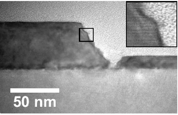
Figure 3 Cross section TEM image of the nominally 20 nm thick AlxGa1-xN
film. The image was taken along the [0110] zone axis and shows a trench between a thinner and a thicker island. The insert is a
magnification of the area indicated by the black rectangle in the image. 73
Figure 4 EDS analysis of the nominally 20 nm thick AlxGa1-xN film. (a) The
STEM image of the mapped region. The grayish areas overlapping the image are caused by electron beam induced contamination. (b)
GaKαmapping. (c) A line scan of the GaKα signal intensity taken along the line indicated by an arrow in (a).
74
Figure 5 (a) Bright field TEM cross-section image of the nominally 100 nm thick AlxGa1-xN film. (b) EDS mapping of the AlKα intensity of the
region shown in (a).
75
Figure 6 (a) Dark field STEM image of a nominally 1 µm thick AlxGa1-xN film.
(b) EDS mapping of the AlKα intensity in the same region. 76 Figure 7 Plan-view TEM bright field images of nominally (a) 20 nm and (b) 60
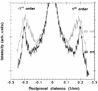
nm thick AlxGa1-xN films on 6H-SiC(0001) showing Moiré patterns
formed due to the lattice mismatch between the film and the substrate. Inserts show the FFT of the respective images.
77
Figure 8 (a) Line scans crossing the first order reflections of the FFT patterns obtained from the plan view TEM images of the nominally 20 and 60 nm thick AlxGa1-xN films.
78
Figure 9 Moiré lattice parameter calculated from Eqn. 1 as a function of Al mole fraction for varying twist angles. The plotted points represent the experimentally observed Al mole fractions of 0.035 and 0.25.
xiii
Figure 10 Geometrical arrangement of Al-rich domains assumed for finite element simulations. (a) In-plane arrangement in a single layer of the two domains. (b) Cross-section of two layers separated by a spacer layer for vertical correlation and anticorrelation of the Al-rich domains.
80
Figure 11 Total strain energy as determined from FE simulations for the vertically correlated (filled circles) and anticorrelated (open circles) arrangement of Al-rich domains in an Al-poor matrix as a function of the spacer layer thickness. The latter is given in units of the height, h, of the Al-rich domains.
81
Figure 12 Schematic of the proposed model for the film evolution during the early stage of growth of AlxGa1-xN on SiC as discussed in the text. The
gray levels represent the Al content with darker areas corresponding to higher Al mole fractions. The solid and light arrows indicate the growth of Al-poor and Al-rich domains, respectively. Their length symbolizes the relative growth rates.
82
Chapter 5
Figure 1 10x10 µm AFM height image of as-received 6H-SiC(0001) wafer showing polishing scratches present on the surface. The vertical height scale is given in the upper right corner of the image.
110
Figure 2 2x2 µm AFM height images of a mechanically polished 6H-SiC(0001) substrate (a), AlN(0001) layers on mechanically polished SiC
substrates ((b) and (c)), hydrogen-etched 6H-SiC(0001) substrate (d), and AlN(0001) layers on hydrogen-etched SiC substrates ((e) and (f)). The nominal AlN layer thickness, based on established growth rates, is given in the upper left corner of each image and the vertical height scale is given on the upper right. A polishing scratch into which AlN islands have grown is indicated by the arrows in (b). The arrows in (d) indicate the edges of unit cell height steps in the hydrogen-etched SiC substrate to which continuous strings of AlN islands have attached.
111
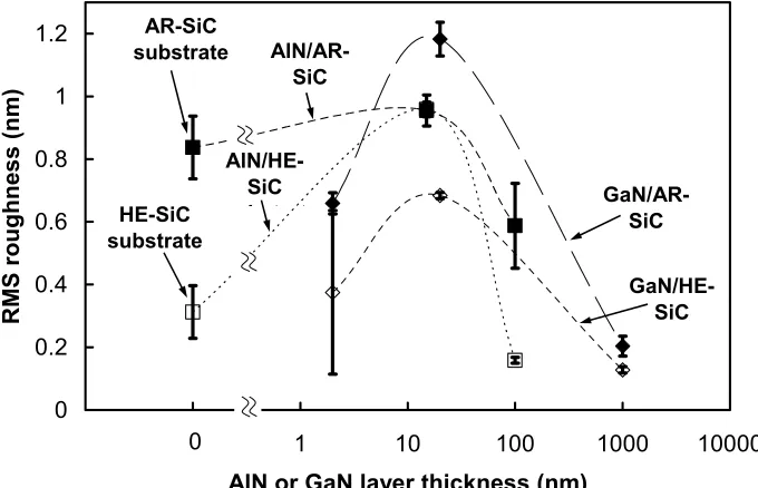
Figure 3 Root mean square (RMS) surface roughness of AlN layers of different thickness and GaN layers of different thickness on 100 nm AlN buffer layers. Results for both as-received (denoted AR-SiC) and hydrogen-etched (denoted HE-SiC) SiC substrates are shown. The plotted points are the average of several measurement locations on multiple samples and the error bars represent the range of values typically observed. The broken lines are a guide to the eye.
112
Figure 4 Cross-sectional TEM imageof a 15 nm AlN film on a hydrogen-etched SiC substrate.
113 Figure 5 Plan-view weak-beam dark-field TEM image of a 100 nm thick AlN
layer on a hydrogen-etched SiC substrate.
Figure 6 Cross-sectional weak-beam dark-field TEM images of a 100 nm thick AlN layer on a hydrogen-etched SiC substrate. The images were acquired from the same region of the film but with varying g-vectors (given in the images).
115
Figure 7 (a)-(i) 2x2 µm AFM height images of GaN layers grown on 100 nm AlN buffer layers. (a)-(c) is for layers deposited on as-received mechanically polished 6H-SiC(0001) substrates. (d)-(i) is for layers deposited on hydrogen-etched SiC substrates. (d) and (g)-(i) are different areas of the same sample with 3, 0, 1 and 2 spiral hillocks observed respectively (arrowed in (g)-(i). The layer thickness is based on established growth conditions and is listed in the upper left corner of each image. The vertical height scale is given in the upper right corner of each image. Note the GaN islands observed in (a), (d), (h) and (i) and the step terminations indicated by arrows in (c) and (f).
116
Figure 8 Plots of the FWHM of X-ray rocking curves obtained at five inclination angles in GaN films deposited on as-received and
hydrogen-etched SiC substrates. The plotted points were obtained in the manner of reference 55 to remove the effect of the misaligned SiC substrate domains. Line fits are a guide to the eye.
117
Figure 9 Cross-sectional weak-beam dark-field TEM image of a 1000 nm GaN/100 nm AlN/hydrogen-etched SiC heterostructure.
118 Figure 10 Plan-view TEM image of a 1000 nm GaN/100 nm
AlN/hydrogen-etched SiC heterostructure showing a TD density of ~1.4x109 cm-2.
119
Chapter 6
Figure 1 Schematics of epitaxial lateral overgrowth (a,d,g),
pendeo-epitaxy(b,e,h) and cantilever epitaxy (c,f,i). Each process is shown for a typical substrate material starting with the template structure and proceeding to coalescence. The arrows in (d-f) indicate the directions of growth as both lateral and vertical.
180
Figure 2 Process flow for a proposed route towards freestanding GaN substrates produced by HVPE growth and separation from a Si(111) substrate. Note that (c) is at the HVPE growth temperature and (d) is at room temperature. The arrow in (d) denotes a crack in the silicon stripe which may form during cooling from the growth temperature. Note that the Si stripes are expected to bend due to the 57% mismatch in the coefficients of thermal expansion between GaN and Si.
181
Figure 3 Mechanics model for determination of the displacement of Si stripes and bending stress in the stripes. The structure is shown at the growth temperature in (a) and at room temperature in (b) and (c).
xv
Figure 4 Deflection of a Si stripe in cantilever epitaxy due to the mismatch in the coefficients of thermal expansion between GaN and Si, as
described by equation (9). The Si stripe is 2 µm wide, 10 µm high, and separated from its neighboring stripe by 5 µm. The thick GaN film and Si substrate are at the top and bottom of the figure respectively. The total deflection, i.e. the separation of the top and bottom of the stripe in the x-direction, is 12.1 nm for this stripe geometry.
183
Figure 5 Contour plot of the of the bending stress in a Si stripe following HVPE GaN growth and cooling to room temperature. The thick GaN film is at the top and the Si substrate is at the bottom. Positive values of stress indicate tension.
184
Figure 6 Maximum bending stress in a silicon stripe at room temperature calculated from equation (14) as a function of stripe width for (a) three different stripe spacings and (b) three different stripe heights. The stripe height and stripe spacing are fixed at 10 µm in (a) and (b) respectively. The horizontal broken line in (b) represents the average fracture stress for Si microcantilevers as measured by Wilson and Beck [44].
185
Figure 7 Outputs of the finite element model of the cantilever GaN/Si structure. The stripe geometry is the same as for Figs. 4 and 5. (a) is a vector plot in which the arrows show the deflection of the stripe from the original location, resulting in a total stripe deflection of 13 nm. (b) is a close-up of the top left corner of the righthand stripe and shows the bending stress at each cell in the model. The white cell denotes the position of the maximum tensile bending stress, which has a magnitude of 99.1 MPa.
186
Figure 8 Cross sectional SEM image of a Si stripe after patterning and dry etching. The photoresist mask is still present on the top of the stripe. Note the scalloping on the sidewalls as a result of the alternating etch/passivation cycles.
187
Figure 9 Cross-sectional SEM micrographs of GaN grown on Si by the
cantilever epitaxy technique. The nominal stripe heights (etch depths) are 5, 10, and 20 µm for (a-c) respectively. The arrows in (a-c) point in the direction of rotation during growth, indicating that the leading edge of the rotation features increased deposition on the Si sidewall. The arrow in (d) denotes the presence of AlN on the sidewall.
188
Figure 10 (a-c) SEM micrographs of GaN grown on etched Si substrates at growth temperatures of 1015°, 1060°, and 1100°C respectively. The images are profile views so that both the cross section and surface are observed. The corresponding lateral and vertical growth rates are plotted as a function of temperature in (d).
Figure 11 (a-e) profile-view SEM micrographs of GaN layers deposited on etched Si substrates. The layers were grown at a constant temperature of 1060°C and the V/III ratio was varied from the standard condition shown in (e). In (a) and (c), the V/III ratio was increased by
decreasing the TEG flow rate while holding the NH3 flow rate
constant. In (b) and (d) the NH3 flow rate was varied. The V/III ratio
and method of increase relative to (e) are shown in the upper left corner of each image and the corresponding lateral and vertical growth rates are plotted as a function of V/III ratio in (f).
190
Figure 12 (a) Growth rates of GaN in cantilever epitaxy on Si as a function of the normalized surface length, Λ, as defined in equation (15). All samples were deposited at 1060°C and V/III=2650 by increasing the flow rate of NH3. Dashed lines are linear least squares fits. The open data point
for Λ=1 represents the vertical growth rate of GaN for these growth conditions on planar Si substrates. (b) is a cross sectional SEM micrograph of a GaN layer deposited on an etched Si template with Λ=0.23 showing that the GaN does not deposit along the entire sidewall when the space between stripes is small.
191
Figure 13 HRXRD triple axis reciprocal space plots of the GaN(0002) reflection for GaN grown by cantilever epitaxy on Si. The incident x-ray beam is directed parallel and perpendicular to the Si stripe direction in (a) and (b) respectively.
192
Figure 14 Cathodoluminescence of GaN films grown by cantilever epitaxy on Si substrates. Room and reduced temperature spectra are given in (a) and panchromatic and band-edge CL maps are shown in (c) and (d)
respectively. The region from which the CL maps were acquired is shown in the plan view SEM image (b).
193
Figure 15 The presence of regions of locally higher Si concentration as
evidenced by a CL map of the donor-acceptor-pair peak, EDS map of the Si Kα peak, and xxx µm AFM height image in (a), (b) and (d) respectively. (d) represents the EDS map of the Ga Lα1 peak.
194
Figure 16 (a)Cross sectional bright field transmission electron microscopy image of GaN grown by cantilever epitaxy on Si substrates and aligned to the
] 12 1
[ zone axis of Si. The black arrows indicate a carbon-based filler material employed during sample preparation. (b) A magnified TEM image of a GaN wing, where the black arrows indicate dislocations on the GaN basal plane and the white arrow indicates the edge of the AlN buffer layer from which the GaN has grown laterally. (c) Slected area diffraction pattern from the GaN/AlN/Si interface.
xvii
Figure 17 Deposition of GaN/AlN on the sidewall of an etched Si substrate. (a) A cross sectional bright field TEM image along the Si [112] zone axis with arrows indicating planar defects believed to correspond to
stacking faults. (b) Selected area diffraction pattern from the GaN on the sidewall superimposed over the Si pattern. (c) SEM image of the sidewall shown in cross section in (a). (d and e) SEM images of the sidewall 100 nm of AlN and 200 nm of GaN deposition respectively. (f) Schematic of the growth process occurring on the sidewall.
196
Figure 18 (a) Plan-view SEM image of two Si stripes, one of which features a roughened surface. (b) Profile view SEM image showing the presence of a void in the Si substrate beneath an area featuring the rough
surface. (c) EDS spectrum acquired from the region in (a). (d and e) EDS maps of the Ga Lα1 and Si Kα signals as acquired from the region shown in (a).
197
Figure 19 (a and b) STEM images of GaN layers featuring smooth and rough surfaces respectively. The inset of (b) is a selected area diffraction pattern observed from the deposit on top of the Si stripe. (c and d) EDS spectra acquired from the GaN layer in (a) and regions “A” and “B” in (b) respectively. (f-h) EDS maps of the Ga Lα, Si Kα, and N Kα signals acquired from the region shown in the STEM image (e).
198
Figure 20 (a-c) SEM images of a cracked GaN film on a planar Si substrate, a subsequently annealed cracked GaN film, and a GaN layer re-grown on a cracked GaN template respectively. The arrows in (a) indicate the ends of cracks traversing the GaN surface. (d) Profile view SEM image of the sample in (c) showing voids in the Si substrate beneath the cracks. (e) XPS spectra acquired from the layers shown in (a-c).
199
Figure 21 (a-d) Schematic showing the process by which Si diffuses from the substrate to the GaN surface resulting in the formation of SixNy and
subsequent GaN overgrowth. (e) 1x1 µm AFM height image of GaN deposited over a Si stripe. The white islands occur at the termination of heterogeneous steps and are believed to correspond to the early stages of SixNy formation on the surface. (f) SEM image showing GaN
overgrowing the SixNy on the surface.
200
Figure 22 The percentage of the cantilever GaN surface degraded due to SixNy
formation as a function of GaN growth time for three different AlN buffer layer thicknesses. The lines are guides to the eye.
201
Figure 23 Plan view SEM images of two cantilever GaN samples near coalescence. The “s” denotes the regions of deposition over the Si stripe and the broken lines indicate the boundary between the GaN over the stripe and the laterally grown GaN wings.
Figure 24 a) Plan-view SEM micrograph of CE-GaN template. b) SEM micrograph showing the surface and cross-section of a GaN layer grown by IVPG which spontaneously separated from the Si substrate during cooling. The original substrate was located toward the bottom of the layer as it is oriented in (b). c) Magnified view of the former interface between GaN/AlN and Si showing that the Si stripes have completely diffused into the growing film, leaving surface voids in their former location.
203
Chapter 7
Figure 1 SIMS depth profiles of H, C. and O acquired from [0001]-oriented GaN-film/GaN-template heterostructures in which the template was heated to 1020°C in a mixture of either (a) nitrogen and hydrogen or (b) ammonia and hydrogen prior to the homoepitaxial growth of the films having a nominal thickness of 0.22 µm.
219
Figure 2 AFM images acquired using 5 x 5 µm scans of the (0001) surface of a GaN template (a) before and (b) after being heated, annealed for 5 minutes and cooled in an ammonia/hydrogen atmosphere. The Z range is 4 nm in each case.
220
Figure 3 AFM images acquired using 5 x 5 µm scans of the (0001) surfaces of homoepitaxial GaN films deposited on GaN templates previously heated to 1020°C in (a) nitrogen and hydrogen and (b) ammonia and hydrogen. The Z range is 5 nm in each case.
221
Figure 4 SEM images showing both the surface and cross section of GaN templates subjected to the following heat treatments: (a) heating in nitrogen/hydrogen to 1020°C and cooling in ammonia/hydrogen, (b) heating in nitrogen/hydrogen to 1020°C, annealing 5 minutes, and cooling in ammonia/hydrogen, (c) heating in nitrogen/hydrogen to 1020°C and cooling in nitrogen/hydrogen, (d) heating in
nitrogen/hydrogen to 1020°C, annealing 5 minutes, and cooling in nitrogen/hydrogen. The hexagonal pits are the result of GaN decomposition. Note the Ga droplets within pits shown in (d).
222
Figure 5 5x5 µm AFM scans of GaN templates after (a) heating in
nitrogen/hydrogen to 1020°C and cooling in ammonia/hydrogen, (b) heating in nitrogen/hydrogen to 1020°C, annealing 5 minutes, and cooling in ammonia/hydrogen, (c) heating in nitrogen/hydrogen to 1020°C and cooling in nitrogen/hydrogen, (d) heating in
nitrogen/hydrogen to 1020°C, annealing 5 minutes, and cooling in nitrogen/hydrogen. The Z ranges are 15, 15, 30, and 100 nm for the respective images. (a) and (b) show a thin GaN-containing layer formed via reaction of liquid Ga with ammonia. (c) and (d) show a decomposed roughened GaN surface.
xix
Figure 6 5x5 µm AFM scans of GaN templates exposed to 30% HNO3 for 10
minutes following (a) heating in nitrogen/hydrogen to 1020°C, annealing 5 minutes, and cooling in ammonia/hydrogen, and (b) in nitrogen/hydrogen to 1020°C and cooling in nitrogen/hydrogen. The Z ranges are 15 and 30 nm respectively. (a) reveals the roughened GaN surface after removal of the thin GaN-containing layer observed in figure 5 (b). (b) shows that the roughened surface formed upon
heating in the absence of ammonia is unaffected by exposure to HNO3.
224
Appendix 1
Figure 1 2x2 µm AFM height images of 100 nm AlN films deposited on Si(111) previously exposed to Al pre-flows of 0 (a), 10 (b), 20 (c) and 30 seconds (d). Respective RMS roughness values are 3.6, 1.0, 4.9 and 3.4 nm.
242
Figure 2 500x500 nm AFM surface plots of 30 seconds AlN deposition on Si(111) previously exposed to Al pre-flows of 0 (a) and 10 seconds (b).
243 Figure 3 5x5 µm AFM height images of 0.5 µm GaN films deposited on 100 nm
AlN buffer layers previously initiated with 0 (a), 10 (b), 20 (c) and 30 second (d) Al pre-flows.
244
Figure 4 RMS roughness of GaN films from Figure 3 vs. Al pre-flow time. Dashed line is a guide to the eye.
245 Figure 5 XRD rocking curve FWHM for three GaN reflections vs. Al pre-flow
time. Dashed lines are a guide to the eye. Error bars represent plus and minus one standard deviation from the mean.
246
Figure 6 FWHM of GaNHRXRD rocking curves for three inclination angles for the cases of no Al pre-flow and 10 second Al pre-flow. Dashed lines are a guide to the eye.
2
Gallium nitride (GaN), in conjunction with the alloys it forms with aluminum nitride
(AlN) and indium nitride (InN), is a semiconductor of considerable interest for optoelectronic
and electronic devices. The theoretical ability to tailor the direct bandgaps of this alloy
system from 0.8-6.2 eV makes it suitable for light emission and detection applications
ranging from the red to the deep ultra-violet (UV) regions of the electromagnetic spectrum.
Light emitting diodes (LEDs) based on III-Nitride materials emitting from green to UV have
been commercialized over the last decade [1]. The visible LEDs are well suited to indicator
applications such as automotive lights and traffic signals as well as in the development of full
color displays. UV LEDs are finding commercial and theoretical applications in bio-agent
detection, air and water purification, and medical treatment and diagnosis. The excitation of
phosphors to produce white light represents a potentially lucrative market for UV LEDs since
illumination accounts for approximately twenty percent of the world’s electricity
consumption [1]. Current white LEDs are twice as efficient as incandescent bulbs yet
emitters in laboratories have demonstrated a tenfold increase in efficiency [1]. The wide
bandgap energies of the III-Nitrides also make them suitable for laser diodes and optical
detectors operating at short wavelengths. The former will enable increased optical data
storage compared to the current AlxInyGa1-x-yP devices and also serve in medical applications
while the latter can function as solar blind detectors for combustion monitoring, fire and
In addition to optical applications, the large dielectric breakdown field, high electron
saturation velocity, and good thermal conductivity of GaN, as well as its alloys, make it an
attractive materials system for high-power, high-temperature, and high-frequency electronic
devices. These devices are expected to serve as amplifiers in radar, missile and satellite
systems as well as in wireless base stations, automotive and avionic applications.
Despite the realized and potential applications for GaN, full exploitation of this
material has been hindered by the lack of mono-crystalline GaN wafers to serve as
homoepitaxial substrates for the growth of films and device structures. Instead, researchers
have been forced to deposit GaN heteroepitaxially on substrates such as sapphire (α-Al2O3),
silicon carbide (SiC) and silicon (Si). Although devices have been commercialized on Al2O3
and SiC and are nearing commercialization on Si, the mismatches in lattice parameter and
coefficient of thermal expansion between the film and substrate generate threading
dislocations (TDs) with densities approaching 1010 cm-2. Combined cathodoluminescence
(CL) and atomic force microscopy (AFM) studies [2,3] have shown that TDs act as
non-radiative recombination centers in GaN. Sugahara et al. [4] provided further evidence of the
non-radiative nature of TDs by observing a one-to-one correspondence between TDs in
transmission electron microscopy (TEM) and dark spots in CL.
Electronic structure calculations of TDs in GaN have shown that they are also likely
to cause deep levels and shallow states in the forbidden bandgap [5,6,7]. Leung et al. [8]
showed that the semi-insulating behavior of high-TD density GaN can be attributed to the
absence of free carriers due to trapping by these levels but for high dopant densities and/or
4
scattering centers in doped material through the use of transverse mobility measurements and
scanning capacitance microscopy respectively. The concept of carrier scattering by charged
dislocation lines is a well known phenomenon in semiconductor physics and results in
degraded performance of electronic devices.
A growing body of evidence also shows that TDs provide a leakage current pathway
and shorten the lifetime of laser diodes. Heterojunction bipolar transistors [11], p-n junctions
[12], and LEDs [13] demonstrate leakage current reductions of ~3-4 orders of magnitude
when the TD density in the III-Nitride layers is reduced. However, high TD densities are
especially detrimental to the performance of more complex and demanding structures such as
laser diodes operating at high power densities [14], as evidenced by the dramatically
increased lifetime for these devices when deposited on low dislocation density templates
[15].
In light of the multitude of deleterious effects of TDs, the current research was
undertaken with the goals of:
1) understanding the evolution of the surface and defect microstructures and strain in
GaN during metalorganic vapor phase epitaxy (MOVPE) growth with various buffer
layers on various substrates
2) exploring a simplified technique of lateral overgrowth for reducing the dislocation
density of GaN on Si substrates
3) employing lateral overgrowth in conjunction with the deposition of thick layers by
hydride vapor phase epitaxy (HVPE) to achieve freestanding pseudo-bulk GaN
substrates
In chapter 2, the growth modes and the microstructures of the surfaces and the defects
generated during the initial and subsequent stages of MOVPE growth of AlN(0001) films on
6H-SiC(0001) substrates and GaN(0001) films on AlN/SiC(0001) substrates are investigated
using atomic force microscopy and cross-sectional and plan-view transmission electron
microscopy. SiC represents an attractive alternative substrate to sapphire due to its easier
cleavage along [1120] and higher thermal conductivity (4.9 W/cm K [16] vs. 0.23 W/cm K
[17] for sapphire). The greater value of the latter property is believed to contribute to the
improved performance of ultraviolet light emitting diodes [18] and heterojunction field effect
transistors [19,20] fabricated in III-Nitride material structures grown on SiC substrates
compared to that of similar devices fabricated on sapphire substrates.
Chapter three builds upon the above research by also examining the surface
microstructure of Al15Ga85N buffer layers and subsequently deposited GaN films on 6H-SiC
substrates. In addition, the evolution of the strain in the GaN as a function of layer thickness
and buffer layer type (i.e. AlN vs. Al15Ga85N) is investigated via high resolution X-ray
diffraction. Although the mismatch in the coefficients of thermal expansion between GaN
and SiC would predict the residual strain to be tensile in nature, the results show that films
can be compressively strained due to a long-range relaxation of the coherent stain between
GaN and the buffer layer. The microstructure and phase separation of Al15Ga85N layers on
6H-SiC substrates is explored in greater detail via TEM, AFM, energy dispersive X-ray
spectroscopy (EDS), and finite element analysis in chapter 4.
Despite the apparent benefits of SiC substrates, namely reduced lattice parameter and
6
proposed for this discrepancy is the damaged surface of as-received SiC wafers as a result of
slicing from the boule, lapping and polishing. Therefore, in chapter 5, AlN films and GaN
films with AlN buffer layers were deposited on 6H-SiC substrates previously etched in
flowing hydrogen at high temperature. This process results in the complete removal of
mechanical polishing scratches and leaves unit-cell-height steps on the SiC surface. The
surface and defect microstructures of the subsequently deposited layers were investigated
using AFM, HRXRD, and plan-view and cross-sectional TEM.
In an effort to reduce the TD density in GaN films, various techniques of lateral
overgrowth have been developed which make use of the anisotropy in growth rates of GaN
along different crystallographic directions. These techniques include epitaxial lateral
overgrowth [21], pendeo-epitaxy [22], and cantilever epitaxy [23]. The research described in
chapter 6 investigates cantilever epitaxy on Si substrates due to the ease of processing the
latter material and the ease with which it can be removed from the backside of a thick layer
by wet etching. The primary goal of the research was to use GaN layers deposited via the
cantilever epitaxy technique as templates for thick GaN layers grown by HVPE. In that aim,
an analytical mechanics model was developed to predict the stress and strain which
developed in the Si stripes as the structures were cooled from the growth temperature. This
model was supported by a finite element simulation. The GaN template layers were
extensively characterized by scanning electron microscopy, AFM, HRXRD, TEM, EDS,
scanning transmission electron microscopy and X-ray photoelectron spectroscopy.
Finally, in chapter 7, a process route previously developed by Tracy et al. [24] for the
cleaning of GaN surfaces in a molecular beam epitaxy chamber in flowing ammonia is
wafers, the latter derived via laser lift-off [25] or the cantilever epitaxy technique developed
in chapter 6, exposed to the ambient acquire a contamination layer containing carbon and
oxygen [26,27]. These impurities have a deleterious effect on the properties of films [28]
and of metal contacts [29,30] subsequently deposited on the contaminated surface.
Secondary ion mass spectroscopy is used to quantitatively analyze the contamination present
at a buried interface and SEM and AFM are used to verify the preservation of the GaN
surface during the cleaning procedure and assess the effect of different heating ambients on
8 1.1 REFERENCES
[1] Gibart P, Rep Prog Phys 2004;67:667.
[2] Rosner SJ, Carr EC, Ludowise MJ, Girolami G, Erikson HI, Appl Phys Lett
1997;70:420.
[3] Rosner SJ, Girolami G, Marchand H, Fini PT, Ibbetson JP, Zhao L, Keller S, Mishra
UK, DenBaars SP, Speck JS, Appl Phys Lett 1999;74:2035.
[4] Sugahara T, Sato H, Hao M, Naoi Y, Kurai S, Tottori S, Yamashita K, Nishino K,
Romano LT, Sakai S, Jpn J Appl Phys Part 2 1998;37:L398.
[5] Elsner J, Jones R, Sitch PK, Porezag VD, Elstner M, Frauenheim T, Heggie MI, Oberg
S, Briddon PR, Phys Rev Lett 1997;79:3672.
[6] Wright AF, Furthmuller J, Appl Phys Lett 1998;72:3467.
[7] Wright AG, Grossner U, Appl Phys Lett 1998;73:2751.
[8] Leung K, Wright AF, Stechel EB, Appl Phys Lett 1999;74:2495.
[9] Look DC, Sizelove JR, Phys Rev Lett 1999;82:1237.
[10] Hansen PJ, Strausser YE, Erickson AN, Tarsa EJ, Kozodoy P, Brazel EG, Ibbetson JP,
Mishra UK, Narayanamurti V, DenBaars SP, Speck JS, Appl Phys Lett 1998;72:2247.
[11] McCarthy L, Smorchkova I, Xing H, Fini P, Keller S, Speck JS, DenBaars SP, Rodwell
MJW, Mishra UK, Appl Phys Lett 2001;78:2235.
[12] Kozodoy P, Ibbetson JP, Marchand H, Fini PT, Keller S, Speck JS, DenBaars SP,
Mishra UK, Appl Phys Lett 1998;73:975.
[13] Sasaoka C, Sumakawa H, Kimura A, Nido M, Usui A, Sakai A, J Cryst Growth
1998;189:61.
[15] Nakamura S, Senoh M, Nagahama S-I, Iwasa N, Yamada T, Matsushita T, Kiyoku H,
Sugimoto Y, Kozaki T, Umemoto H, Sano M, Chocho K, Appl Phys Lett 1998;72:211.
[16] Slack GA, J Appl Phys 1964;35:3460.
[17] Liu L, Edgar JH, Mater Sci Eng R 2002;37:61.
[18] Adivarahan V, Chitnis A, Zhang JP, Shatalov M, Yang JW, Simin G, Khan MA, Appl
Phys Lett 2001;79:4240.
[19] Rumyantsev S, Levinshtein ME, Gaska R, Shur MS, Yang JW, Khan MA, J Appl Phys
2000;87:1849.
[20] Sun J, Fatima H, Koudymov A, Chitnis A, Hu X, Wang H-M, Zhang J, Simin G, Yang
J, Khan MA, IEEE Electron Device Lett 2003;24:375.
[21] Beaumont B, Vennéguès P, Gibart P, Phys Stat Sol (b) 2001;227:1.
[22] Roskowski AM, Preble EA, Einfeldt S, Miraglia PM, Davis RF, IEEE J Quantum
Electron 2002;38:1006.
[23] Ashby CIH, Mitchell CC, Han J, Missert NA, Provencio PP, Follstaedt DM, Peake GM,
Griego L, Appl Phys Lett 2000;77:3233.
[24] Tracy KM, Mecouch WJ, Davis RF, Nemanich RJ, J Appl Phys 2003;94:3163.
[25] Paskova T, Darakchieva V, Paskov P, Sodervall U, Monemar B, J Cryst Growth
2002;246:207.
[26] King SW, Barnak JP, Bremser MD, Tracy KM, Ronning C, Davis RF, Nemanich RJ, J
Appl Phys 1998;84:5248.
[27] Prabhakaran K, Andersson TG, Nozawa K, Appl Phys Lett 1996;69:3212.
10
2. Surface and defect microstructure of GaN and AlN on
6H-SiC(0001) substrates
Z.J. Reitmeier, S. Einfeldt and R.F. Davis
Department of Materials Science and Engineering, North Carolina State University, Raleigh, North Carolina 27695
X. Zhang, X. Fang, S. Mahajan
Department of Chemical and Materials Engineering, Arizona State University, Tempe, Arizona 85287
12 2.1 ABSTRACT
The growth modes and the microstructures of the surfaces and the defects generated
during the initial and subsequent stages of growth via metalorganic vapor phase epitaxy of
AlN(0001) films on 6H-SiC(0001) substrates and GaN(0001) films on AlN/SiC(0001)
substrates were investigated using atomic force microscopy and cross-sectional and
plan-view transmission electron microscopy. Partially coalesced islands of AlN were present after
nominally ~15 nm of growth. Increasing the thickness to 100 nm resulted in complete island
coalescence and the formation of undulating films as a result of the polishing scratches in the
SiC substrate and a surface microstructure containing steps, terraces and small pits. The
AIN/SiC interfaces showed steps delineated by misfit dislocations and a complex misfit
dislocations network. The 100 nm AlN layers exhibited reduced dislocation density as
compared to the 15 nm layers. GaN initially grew in the Stranski-Krastanov growth mode on
100 nm thick AlN buffer layers with islands forming preferentially within the undulations of
the AlN. Complete coalescence of these islands occurred at thicknesses less than 100 nm,
and the subsequently deposited film grew via dislocation-mediated step-flow. Threading
dislocations TDs in A1N were replicated into GaN overgrowths. The density of TDs in GaN
2.2 INTRODUCTION
The lack of readily availablemonocrystalline GaN boules from which wafers can be
obtained has necessitated the growth of GaN films and device material structureson
substrates such as sapphire (α-Al2O3) and silicon carbide(SiC). The mismatches in lattice
parameters and coefficients ofthermal expansion between aGaN film and either ofthese
substrates result in high densities (~108-1010 cm-2) of misfit and threading dislocations (MDs
and TDs). The latter introduce intergap states that serve as non-radiative recombination
centers, act as charged scattering centers, and provide leakage current pathways [1]. It is
therefore important to determine the origins and the evolution of these defects to more
effectively control their type, density and distribution within the heteroepitaxial III-Nitride
films. A large body of literature exists that addresses these topics for dislocations in
III-nitride thin films deposited on the (0001) surface ofsapphire substrates(see, e.g.refs. 2, 3
and the references therein). Three types of TDs have been reported: pure edge (a type:
b=1/3<1120>), pure screw (c type: b=[0001]) and mixed (c+a type: b=1/3<1123>). Two
mechanisms have been proposed to explain the generation of these TDs. Ning, et al. [4] and
Wu, et al. [5] haveclaimed that the TDs formed as a result of local tilt and twist at the
boundaries between coalescing GaN islands. However, these investigators were unable to
demonstrate visual evidence of this phenomenon. More recently, Narayanan and coworkers
[6,7] have demonstrated two alternative sources of TD generation: planar defects in the
low-temperature GaN nucleation layer and point defects incorporated during growth. The
stacking faults in the nucleation layers were shown to be the major source of defects. These
14
SiC represents an attractive alternative substrate to sapphire due to its easier cleavage
along [1120] and higher thermal conductivity (4.9 W/cm K [8] vs. 0.23 W/cm K [9] for
sapphire). The greater value of the latter property is believed to contribute to the improved
performance of ultraviolet light emitting diodes [10] and heterojunction field effect
transistors [11,12] fabricated in III-Nitride material structures grown on SiC substrates
compared to that of the same devices fabricated on sapphire substrates. Deposition of GaN
directly on SiC(0001)substrateshas been accomplished via plasma-assisted molecular beam
epitaxy (MBE) [13,14] and metalorganic vapor phase epitaxy (MOVPE) [15,16]. However,
these films typically suffer from rough surfaces, higher TD density and/or biaxial tensile
strain, which may result in cracking of the films even for relatively small thicknesses. This
tensile strain has beenattributed to the mismatch in thermal expansion coefficients between
GaN and SiC [17] and hasa magnitude of -0.1% in GaN films grown at 1000°C [18].
Alternatively, the microstructural and electronic properties of GaN films deposited on
SiC have been improved by inserting a high-temperature(≈1100°C) AlN buffer layer prior to
GaN deposition [19,20]. This practice facilitates the nucleation of the subsequently
deposited GaN film, allowing fully coalesced films at smaller thicknesses. The lattice
mismatch between AlN and GaN (+2.5%) results in films of the latter material whose volume
is compressively strained when deposited on SiC substrates, despite the counteracting
volume tensile strain generated by the differences in the coefficients of thermal expansion
[17]. Thus, the tendency for crack formation within the heterostructures is reduced. This
residual compression results from a long-range two-step relaxation of the coherent strain as
performance of high electron mobility transistors by inhibiting parasitic substrate conduction
[22].
The transmission electron microscopy (TEM) investigations of Tanaka [23] and
Torres [24] of AlN(0001) thin film/SiC(0001) substrate heterostructures revealed TDs having
densitiesof 1011-1012 cm-2 and composed predominantly of a type dislocations. Numerous
investigators (see, e.g., refs. 25 and 26) have also reported high TD densities in
GaN/AlN/SiC assemblies. However, these studies have usually presented results for one
thickness of GaN film deposited on one thickness of the AlN buffer layer. In contrast to the
GaN/sapphire heterostructures, those composed of GaN/AlN/SiC and AlN/SiC have not been
extensively studied in terms of growth modes and evolving defect microstructures. In the
present research the surface and defect microstructures of the initial and subsequent stages of
growth of AlN on 6H-SiC(0001) and GaN on AlN/SiC heterostructures have been
determined and correlated.
2.3 EXPERIMENTAL PROCEDURE
The AlN was grown via MOVPE at 1100°C and 20 Torr total pressure on the Si-face
of conventionally-polished, on-axis 6H-SiC(0001) wafers, which had been etched in a
HF:H2O (1:10) solution for ten minutes at room temperature to remove the native oxideand
blown dry with nitrogen. The GaN was grown at the same total pressure on 100 nm thick
AlN buffer layers after cooling to 1020°C over a period of five minutes. The MOVPE
reactor was a cold-walled vertical pancake-style system, which was evacuated to 10-6 Torr
prior to growth. The temperature of the SiC-coated graphite susceptor was measured using a
16
diluent. The V/III ratios of 24,400 and 1,300 were employed for the growth of the AlN
layers and for GaN layers thicker than 2 nm; the corresponding growth rates were 0.3 µm/hr
and 1.8 µm/hr, respectively. The TEG/ammonia ratio was increased to 10,600 by decreasing
the flow of the TEG to investigate the initial nucleation and growth of GaN on the AlN to a
maximum thickness of 2 nm. This change reduced the growth rate of the GaN to 0.22 µm/hr.
Atomic force microscopy (AFM) and high resolution X-ray diffraction (HRXRD)
investigations ofGaN layers of the same thickness but deposited using two different growth
conditions did not reveal significant differences. All film thicknesses quoted are nominal
values based on these established growth rates.
The surface microstructure of the heteroepitaxial films weredetermined using a
Digital Instruments D3000 AFM equipped with a Si cantilever and tip operating in the
tapping mode. Cross-sectional samples for transmission electron microscopy (TEM) were
prepared using the standard ‘sandwich’ technique followed by dimpling and ion milling until
electron transparency. Plan-view samples were prepared by cutting 3 mm discs from SiC
substrates. These discs were then ground, dimpled and ion milled from the SiC side to obtain
electron transparency. Structural analyses of the epitaxial layers were preformed in
cross-section and inplan view using a JEM-4000EX microscope operating at 400 kV that has an
2.4 RESULTS AND DISCUSSION
2.4.1 SURFACE MICROSTRUCTURES AND GROWTH MODES OF AlN ON SiC
SUBSTRATES
Representative micrographs of thesurfaces of the polished 6H-SiC(0001) substrates
and the AlN(0001) films with thicknesses of 15 and 100 nm grown in this research are shown
in the AFM images in Fig. 1. The 10x10 µm images reveal the influence of the roughness of
the substrate shown in Fig. 1 (a) on that of the AlN films shown in Figs. 1 (b) and (c). The
2x2 µm images reveal the details of the microstructures of the substrate surface (Fig. 1 (d))
and the AlN layers (Figs. 1 (e) and (f)). Standard mechanical polishing of the surfaces of this
hard, inert and difficult to polish material [27] normally produces numerous randomly
oriented scratches with widths from 100-800 nm and depths to 12 nm, as shown in Figures
1(a) and (d). Our AFM studies did not reveal steps on the surfaces of the as-received SiC
substrates; however, scanning tunneling microscopy studies by Owman et al. [28] have
revealed steps with random heights and orientations.
The 15 nm thick AlN layer nucleated both within and between the scratches of the
SiC substrate, as shown in Figs. 1 (b) and (e). The scratches remainevident in both images.
The depression running from the upper left to the lower right in Fig. 1(e)is a polishing
scratch into which AlN islands have grown. The islandsappear homogeneously distributed
across the surface, indicating that preferential nucleation within the scratches or between the
scratches did not occur. At this nominal thickness, the AlN film is partially coalesced and
composed of islands with random shape and orientation, i.e. the sides of the islands do not
18
image, since the 10 nm radius of the AFM tips is comparable to the lateral size of the islands.
AlN(0001) deposited on 6H-SiC(0001) by MBE grows in the Stranski-Krastanov (S-K)
mode [29] in which a pseudomorphic wetting layer having a thickness of several monolayers
is followed by strain-induced island growth. This growth mode was not observed in our
AFM studies, since the roughness of the SiC substrate made the observation of AlN layers
difficult when growth times shorter than that used to growthe 15 nm samples were
investigated. The polishing scratches in the substrate remained manifest in the film even
after 100 nm of AlN growth, as clearly shown in Fig. 1(c). Straight undulations in AlN have
also been observed by Smart [30], Nishida [31], and Einfeldt [21] and attributed to scratches
in the substrate. One of these scratch-induced undulations in the AlN film is clearly observed
running from lower left to upper right in Fig. 1(f). In contrast to the islands observed for the
15 nm layer and in addition to the undulations, the 100 nm film also exhibits terraces
separated by bi-layer high steps and pits, the latter as a result of incomplete coalescence at
this stage of growth.
2.4.2 DEFECT MICROSTRUCTURE OF AlN ON SiC SUBSTRATES
A (1100)cross-sectional TEM image of a 15 nm AlN film deposited on a
mechanically polished SiC substrate is shown in Fig. 2; the operating reflection is (0002).
The AlN islands have coalesced to form a flat surface, a result consistent with our AFM
studies. The dark bands in the layer and the substrate imply that the composite structure may
not be fully relaxed while the dark regions at the AlN/SiC interface suggest the presence of a
defective structure in this region. Imaging the layer using other reflections proved difficult
Combining these results with those of Fig. 2, we can infer that the most likely Burgers
vectors of dislocations in the AlN layer are 1/3<1120>and may be 1/3<1123>.
Figure 3 shows a plan-view, weak-beam, dark-field (WBDF) image of a 15 nm
AlN/SiC composite. Steps separated by 250-300 nm and delineated by dislocations are
observed. The majority of the steps are aligned close to a <1100> direction. The terraces
between steps are defined by a very dense network of jagged dislocations whose orientations
are not well defined. Results on 100 nm AlN layers deposited on SiC were qualitatively
similar to the preceding results. The major difference was a lower density of dislocations in
the thicker layer.
Results on dislocation-delineated steps and jagged misfit dislocation networks in Fig.
3 are very interesting. They can be rationalized by referring to the schematic shown in Fig. 4.
Ideally, a relaxed (0001) AlN/SiC interface should consist of a hexagonal network of three
perfect edge a type dislocations because the misfit is accommodated most efficiently in this
manner. This situation is shown schematically in Fig. 4(a), where we depict a portion of the
hexagonal misfit dislocation network on a terrace that is bounded by two steps. When we
extend this situation to two terraces, as shown in Fig. 4 (b), it is easy to see the alignment of
misfit dislocations along the step edges.
The jagged structure of misfit dislocations in Fig. 3 could be due to the fact that the
AlN/SiC interface is rough. This could be caused by the non-planarity of as-polished SiC
surfaces. An additional complication could arise from the projection of the defective
20
2.4.3 SURFACE MICROSTRUCTURES AND GROWTH MODES OF GaN ON AlN/SiC
SUBSTRATES
The surfaces of the GaN(0001) films having thickness values from 1-4000 nm and
grown on the 100 nm AlN(0001) buffer layers are shown in the AFM height images of Fig.
5. A comparison of the surface of the nominally 1 nm thick GaN film shown in Fig. 5 (a)
with that of the bare AlN buffer layer shown in Fig. 1 (f) reveals steps and terraces on an
undulating surface in both cases. Three dimensional nucleation of GaN was not observed.
There are two possible explanations for this observation. First, there could be a reduced
growth rate during the initial nucleation compared to the steady-state growth rate, as has been
observed in similar MBE studies [32]. Therefore, the surface shown in Fig. 5 (a) would be
that of the AlN buffer layer. The microstructure of this surface may also be explained by the
pseudomorphic growth of a very thin GaN layer. Close inspection of the two figures reveals
that the step edges in Fig. 5 (a) are smoother and more regular than those of the AlN buffer
layer. It has been determined [33,34,35] that GaN deposited via MBE at sufficiently elevated
temperatures grows in the S-K mode in a manner similar to that of the growth of AlN on SiC
(see above). The thickness of the pseudomorphic wetting layer in the GaN film is reported to
be between 1-5 bilayers[33,34,35].It is therefore reasonable to assume that the S-K mode
will also pertain for the initial growth of GaN via MOVPE. We therefore believe the surface
shown in Fig. 5 (a) is that of the initial two-dimensional layer of GaN growing in the S-K
mode; hence the observed change in the step and terrace structure of the surface as compared
to that of the bare AlN buffer layer.
The strain induced two dimensional-to-three dimensional transition in the S-K growth
GaN islands denoted by arrows in Fig. 5 (b). The majority of the islands observed occurred
in a straight line corresponding to one of the scratch-induced undulations in the AlN surface.
Fig. 4(c) shows a line of GaN islands which have formed on the lower left as well as a few
small islands which appear to have formed at step edges (see arrows). The larger scale image
of the 2 nm GaN layer shown in Fig. 6(a) supports the postulate drawn from the observations
in the smaller scale image that the most prevalent GaN nucleation occurs within the
undulations in the AlN which mimic the linear morphologies of the scratches in the SiC.
Nishida [31] and Koleske [36] have also observed GaN nucleation in the form of aligned
islands when deposited on AlN/SiCsubstrates. Even with a carefully optimized process,
mechanically polished 6H-SiC(0001) wafers possess a damaged region extending8 nm
beneath the surface[37]. Studies of the homoepitaxial growth of SiC on mechanically
polished SiC(0001) substrates have shown locally higher densities of edge and screw TDs in
the areas of the film directly over a polishing scratch [38,39]. Therefore, it is reasonable to
assume that AlN films depositedon SiC substrates will also contain locally higher TD
densities in these highly damaged regions of the substrate. GaN preferentially nucleates in
these areas,since clusters of extended defects in the AlN buffer layer have been shown to
serve as sites for the initial nucleation of GaN [40,41].
The GaN islands of the 5 nm deposit are irregular in shape in a manner similar to that
of the AlN islands grown on SiC, and the sides of the former do not appear to correspond to
any particular crystallographic facets. Observations of single scan lines such as that shown
in the inset of Fig. 5 (d) reveal that the tops of the GaN islands are essentially atomically
(c)-22
the growth mode of the GaN changes from the thermodynamically-controlled S-K mode to
the kinetically controlled and commonly observed dislocation-mediated step-flow growth
mode [42],as evidenced by the roughly parallel array of terraces and steps observed in Fig. 5
(g). The surface microstructure of the1 µm GaN film shownin Figs. 5 (h) and 6 (c) and the
4 µm GaN film in Fig. 5 (i) contain terraces and bilayer high steps. The arrows in Fig. 5(h)
and (i) denote step terminations that are the ends of TDs having screw or mixed character
[42]. From averaging over several AFM images, the density of step terminations for the
respective films is 1x109 cm-2 and 5x107 cm-2, respectively, indicative of the previously
reported reduction in TD density via dislocation annihilation mechanisms as the film
thickness increases [43].
2.4.4 DEFECT MICROSTRUCTURE OF GaN ON AlN/SiC SUBSTRATES
Figure 7 (a) depicts a WBDF image of a cross-section obtained from a 1000 nm
GaN/15 nm AlN/SiC composite. A highly defective region is observed at the AlN/SiC
interface. The thickness of this region is 100 nm; thus it extends well beyond the AlN layer.
However, individual dislocations are not easily discernible in the defective area. A large
number of dislocations come together to form closed loops in the GaN layer near the
GaN/AlN interface. The TDs appear uniformly distributed across the GaN layer but decrease
in density in the direction of film growth. From plan-view TEM the TD density was
determined to be 4.5x109 cm-2.
Figure 7(b) shows an enlargement of a region delineated by an arrow in Fig. 7(a). It is
clear that the highly dislocated area contains a high density of very small dislocation loops
Furthermore, almost all TDs in the GaN layer appear to originate from the defective region
described above.
Figure 7(c) shows an area close to the one shown in Fig. 7 (a), but the operating
reflection is (0002) instead of (1120). Comparing dislocation distributions in Figs. 7 (a) and
(c), it is clear that the majority of TDs are a type and that only a few c and c+a dislocations
are present. In addition, the observed contrast within the AlN layer indicates that it may also
contain some c and c+a dislocations.
The increase in thicknesses of AlN and GaN to 100 and 2000 nm respectively
reduced the density of TDs in the GaN layer. Figures 8 (a) and (b) show cross-sectional
images of a 2000nm GaN/100 nm AlN/SiC sample for two different operating reflections,
) 110 2
( and (0002) respectively. Again there is almost one-to-one correlation between the
TDs in GaN and AlN layers and from comparison of Figs. 8(a) and (b) it is clear that the
majority of the dislocations are a type, but a few c and c+a dislocations are also present. A
typical plan-view TEM image of this GaN layer is shown in Fig. 9. Only a and c+a
dislocations are visible in this micrograph. Furthermore, the TDs appear to form a cellular
structure, and their density is estimated to be 1.5x109 cm-2.
Cross-sectional and plan-view TEM images (not shown) were also obtained for 4000
nm GaN/100nm AlN/SiC heterostructures. As in the case of two previous samples, the
majority of TDs were a type and few c and c+a dislocations were observed. The TD density
was 5.5x108 cm-2, and they were randomly distributed and did not form a cellular pattern.
The highly defective regions, observed at, within, and beyond the AlN/SiC and
24
dislocated SiC substrate; mechanical polishing and scratches increase the density of
dislocations terminating on the SiC surface. Since the lattice parameters of AlN and SiC are
different, misfit-dislocations must be introduced at the AlN/SiC interface when the thickness
of AlN exceeds a critical value. In addition, dislocations terminating at a SiC surface
replicate into the AlN overgrowth. As argued by Beam et al. [44], two distinct situations
could arise for homoepitaxial growth: a Burgers vector inclined to the growth surface or a
Burgers vector parallel to the growth surface. They showed that in both cases dislocations are
replicated into the overgrowth; however the situation for the growth of AlN on SiC is more
complicated since the two materials have different lattice parameters. Mahajan and Sree
Harasha [45] suggested that a dislocation with a Burgers vector b1 in SiC will be replicated
into A1N as a threading dislocation with a Burgers vector b2 and a residual dislocation with
Burgers vector b3 that is left at the AlN/SiC interface, i.e.,
b1(SiC) b2(AlN) + b3 (Interface) (1)
Eq. (1) is generic in nature and should apply to the replication of threading dislocations in
any heteroepitaxial structure. Therefore, this argument can also be used to rationalize the
association of TDs in GaN with those in AlN, Figs. 7 and 8. The distribution of dislocations
observed in Fig. 7 can also be understood. Our assessment is in contrast to that of Moran et
al. [46] who postulated that TDs result from the coalescence of GaN islands when deposited
on AlN/SiC substrates. These authors did not discuss the role that TDs in AlN may have on
the formation of TDs in GaN.
Comparing Figs. 7 and 8, it is apparent that the density of TDs or dislocations in a
100 nm thick AlN layer is much lower than that in a 15 nm layer. This could occur if closely