Nano-Heterostructures Based on Solid
Solution HgCdTe obtained using Silver Ion
Implantation
R.S. Udovytska
1Researcher, Dept. of physical and technological proble ms of semiconductor IR-techniques, V. Lashkaryov Institute of Se miconductor Physics, NAS of Ukraine1
ABSTRACT: Presented in this work are the results concerning format ion of nano -heterostructures Ag2O-Hg1–xCdxTe
(x = 0.2) on the surface of solid solution Hg1–xCdxTe (х ~ 0.223). Modification of this ternary chalcogenide
semiconductor compound was performed using the method of doping the heterostructure samples with silver ions, which was followed by low-te mperature treat ment. The energy and dose of imp lanted ions were 100 ke V and 4.8∙1013 сm-2, respectively. Studied in this work a re e lectro-physical and structural properties of the narrow -band semiconductor compound Hg(Cd)Te with the nano -heterostructure Ag2O-Hg1–xCdxTe (x = 0.2) formed on its surface by
using the method of ion implantation Ag+ ions in the top -down approach. These semiconductor nano-heterostructures were characterized using impedance spectroscopy, AFM-microscopy and photoelectric spectroscopy.
KEYWORDS: Se miconductor, ion implantation, nanostructure, electro-physical, impedance spectroscopy.
I.INTRODUCTION
Nanostructured ele ments consisting of Hg(Cd)Te solid solutions are effectively using in T -devices for far IR and THz ranges [1]. One unique application of se miconductor quantum dots is based on A2B6 compounds (CdHgTe, CdTe/CdSe , CdTe1−xSex/Cd S, HgxCd1−xTe/CdTe/CdxZn1−xS, etc. [2-4]): it is also well known as mu ltispectral
(650…900 n m) fluorescent tomography (MSFI) that is indispensable in biomedicine for early detection of severe diseases. As known, for preparation of nano-materials with unique properties, format ion of hierarchica l structures is required.
The Ag2O film in the work [5] was deposited on the surface by D.C magnetron sputtering at substrate o f room
temperature using an Ag target (99.99% purity) in the Ar atmosphere. The oxygen was introduced during the deposition. The n-type Si(111) wafer was cleaned and then, p-Ag2O was deposited on it. Ag2O is a p-type
semiconductor with direct band gap around 1.4e V, which is appropriate to apply to solar cells. In addition, it is e xpected that this configuration may be used for fabrication of the p-Ag2O/other n-type materia ls heterojunction solar
cell [5].
One of the widely spread methods for modificat ion of structural and mo rphologic characteristics can be
developed by ion imp lantation. In this paper, to form a thin film Ag2O was used method of ion imp lantation Ag ions to
the surface of semiconductor structure Hg(Cd )Te. Using solid solution of n-CdxHg1-xTe (x = 0.22) we can co mb ine the
functional properties of o xide Ag2O (Eg = 1.41 e V) [1] and se miconductor Hg(Cd)Te (Eg = 0.123 e V).
Bo mbard ment of semiconductor with ions, atomic clusters or molecules results in changing thermodynamic parameters and features inherent to surfaces of basic system co mponents. Doping of semiconductors is used for obtaining micro-structured materia ls possessing mu lti-functionality of e lectric, magnetic, optical and other properties. It is enables to control materia l properties through choosing of appropriate irrad iation regimes and conditions for thermal annealing. Several e xa mples of format ion of nano-composites and metal-o xide nano-heterostructures by using ion implantation are represented in [6-9].
That is why we require investigation of electro -physical and structural properties of the narrow -band semiconductor compound Hg(Cd)Te with the nano -heteroarchitecture Ag2O-Hg1–xCdxTe (x = 0.2) formed on its surface
The purpose of this work was development of new physical properties of the solid solution by nanostructurizat ion of Hg(Cd)Te surface by ion implantation and to expand the operating range of the spectral sensitivity.
II.RES ULTS
Ion imp lantation is widely used for the manufacturing of the infrared photodiodes based on Hg(Cd)Te (М СТ) solid solution [10]. The purpose of this work was to study the effect of the B+ and Ag+ ions irradiat ion on the properties of heteroepitaxia l structures Hg(Cd)Te / CdZnTe. In this paper, the surface morphology as well as optical, electrical and photoelectrical properties of Hg(Cd)Te - based heterostructures were investigated. We implanted Hg(Cd)Te /CdZnTe (х=0.223) structures by the method of nonoriented irradiat ion with Ag+ ions. This process was realized on a Vizuviy-5 imp lanter with an imp lantation energy of 100 kе V and a dose of 3*1013 cm-2 with subsequent low-temperature annealing at a low-temperature o f 75ºС in Аr at mosphere under a pressure of 0.4 MPa for 5 h. A ll processed surfaces were exa mined using atomic force mic roscopy (АFМ - NanoScope IIIa Digital Instruments) microscopy (Fig 1 a, b). To provide electro-physical investigations, a mesa-structure was prepared using the chemica l etching of the sample in the standard etchant Br-HBr. Indiu m e lectrodes were deposited on faces of the sample. Impedance characteristics of the samples were studied using the precision impedance meter Z-3000X within the frequency range 1 Hz…3 10 6
Hz with the amplitude of a sinusoidal signal 120 mV (Fig 2, Fig 3, Fig 4 a, b) [11-12]. Photosensitivity spectrum was obtained by spectrometer SPM 2 (Fig 5).
III.DISCUSSION
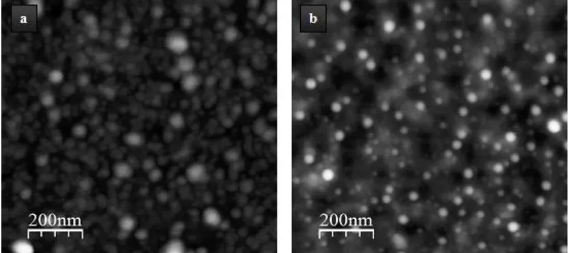
In the previous work [7] AFM images for the samples irradiated B+ ions was studied. Nanostructure was formed by the metod of ion imp lantation MCT, Ag+ ions (Fig. 1a, 1b). The results of topometry based on AFM measurements (Fig. 1a) show the network of quasi-pores with the depth 3.5 to 10 n m and dia mete r 50 to 160 n m as we ll as grains with sizes 40 to 80 n m densely packed in the surface plane. After imp lantation with silver ions (Fig. 1b), on the background of insignificant smea ring of grain boundaries, with ma intenance of in itia l surface porosity, there formed is a un iform array of cone-like spikes with the height h fro m 5 to 25 n m and base dia meter d between 13 to 35 n m.
Fig. 1 A FM image of the film CdхHg1-хTe (х ~ 0.223): a ) initia l surface of the sample; b) after Ag+ imp lantation and
annealing
distortion with comp ression strains ε1 = (aCdHgTe – a0)/aCdHgTe = –4.485×10 –4, a0 = 6.4660 Å [13]. XRD results in the
coherent-scattering region point out to the tension of the silver imp lanted Hg(Cd )Te layers [13]. It is found that the mechanica l stresses that arise in the near-surface layer of an epitaxia l MCT layer attain the ma xima l value of σmax = 2∙105
Pa [7]. Deformations arising after embedding silver ions prevent the process of mercury diffusion in the implanted target.
It is known that mercury migration in MCT is accompanied by the effect of “healing” of vacancy defects - VHg.
In the deformed “vacancy” semiconductor film, the healing effect is absent, which is confirmed by preservation of initia l porosity in MCT sa mples after implantation and the following therma l treat ment. Apparently, transformation of the defect structure in semiconductor film reflects elastic relaxation “compression – extension – compression” in the region of MCT loosened by ion imp lantation [7]. Conditions for appearance and regularities in development of surface pores and cones on solid surface irradiated with ions, in accord with [13], can be expla ined by the processes related with ion-induced strains that arise due to saturation of the surface by embedded silver atoms. The deformation accumulat ion is found to lead to the topological instability of the irrad iated surface. The silver ato ms fill mic roscopic voids in crystal lattice as a result of ion-stimulated diffusion and recombination processes in sub-surface layers. Co mpression of mo re deep layers in the loosened epitaxial film (> 0.04 µm) at the mo ment following after e xtension promotes “deformation squeezing” the silver ions to surface. Silver, as usual, demonstrates high penetration ability and has an aptitude for creation of solid solutions with high liab ility.
Structure modificat ion leads to change electrophysical parameters, such as CV- characteristics. Impedance spectroscopy is a very sensitive method for detection of non -stationary charge transport governed by charge-carrier rela xation in disordered semiconductors structure. Therefore heterostructure CdхHg1-хTe/CdZnTe after Ag+
implantation was characterized by impedance spectroscopy. The value and interpretation of impedance spectra are processed in analogy to equivalent circuits involving simple co mponents such as resistors and capacitors [11]. The impedance measure ments were performed at the G-Cp (para llel conductance and capacitance) configuration using Au plates as blocking electrodes. Using the impedance technique, data equivalent to the real and imaginary parts of comple x e lectrical va lues are measured as a function of the frequency of the applied electric field [11].
Hodographs of impedance for samples obtained by irradiat ion w ith ions B+ and Ag+ were analyzed (Fig. 2, 3). Using the EIS spectrum analy zer [11]according to the Vought approach, we obtained an equivalent circuits presented on Figs. 2, 3. For a sa mple imp lanted by B+ ions obtained dependence was with characteristic diffusion impedance (Fig. 2). He re R1 is the contact resistance, СPE1 – Warburg impedance, series R2-CPE2 – circuit corresponding to the charge transfer and capacitance of the space charge region. For a sa mple imp lanted by Ag+ ions, corresponding dependence was obtained (Fig. 3). He re R2-СPE1 is the paralle l capacitance of the disordered layer. At the same time instead of expected combination R3-CPE2, this circuit corresponds to the charge transfer and the capacitance of the space charge region. СPE3 is changed to a reactive ele ment inductance L. Thus, we detected the presence of "treated materia l" a series R3-L1 for this c ircuit. The important peculiarity of the equivalent circu it was appearance of the inductivity L, wh ich is not typical of semiconductor compounds. Analysis of real part impedance of the initial samples CdxHg1–xTe did not show any presence of capacitance C. A typical Bode plot obtained for sample Ag2O-CdxHg1–xTe is
23,2 23,4 23,6 23,8 24,0 23,4
23,6 23,8
Re(Z),Ohm
-I
m
(Z
),
O
h
m
analog
physical
Fig. 2 Hodograph of the impedance for the heterostructure CdхHg1-хTe (х = 0.223) a fter B+ imp lantation
73,6 74,4
0,0 0,9 1,8 2,7 3,6 4,5
analog
physical
Re(Z),Ohm
-I
m
(Z
),
O
h
m
Fig. 3 Hodograph of the impedance for the heterostructure CdхHg1-хTe (х = 0.223) a fter Ag+ imp lantation
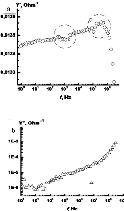
Frequency dependence of real and imaging part of admittance of the system Ag2O-CdxHg1–xTe was analyzed
(Fig. 4a, 4b). Analysis of the real part of ad mittance Y’ (Fig. 4a), the frequency dispersion is not observed within the
range (1 Hz…1 М Hz). Th is behavior of the measured electric circuit indicates presence of some capacitance C. In the low-frequency range (102…104) Hz, the implanted samples show specific features that are indicative on resonance levels of charge transfer processes in structured materia l (first circle Fig. 4a ). The observed sharp drop within the high -frequency range (1…3) МHz (second circle Fig. 4a) can be caused by geometrical and electrical related of the studied samples. The imaginary part of admittance Y’’ has practically very low value, but within the total range of
Fig. 4 a) Frequency dependence of real part of admittance of the heterostructure ;b) frequency dependence of imaging part of admittance of the heterostructure, for the system Ag2O-CdxHg1–xTe (х = 0.223)
Presence of the oxide on the surface of the metal particles Ag is expla ined by equivalent circuit of non -metallic components. Probably, this fact determines the appearance of the other equivalent circuit that describes the behavior of the samples, where additional o xide barrie rs inhibit the current transfer. This e xp la ins the presence of series R2-L1 in the equivalent circuit. The presence of oxygen impurity o n the surface of the implanted layers is explained by adsorption of the residual at mosphere of the vacuum cha mber and distributed in the depth of the target as a result of stimulat ing radiation and thermal diffusion processes. Relat ively high concentrations of impurities introduced the process temperature and the enthalpy of format ion of o xide phases co ntributed to their synthesis under ion irradiat ion. Irregula rit ies presented on the surface of the samples CdxHg1-xTe have an important role in the processes of oxygen
penetration adsorption during ion imp lantation. Thus, the С2 (the capacitance of the space charge region) is converted to the inductance, which is inherent, fo r e xa mp le, to electronic gyrators [12]. In our opinion, the offered way to form the nano-dimensional relief on the surface of the film prepared fro m narrow -band semiconductor is promising for creation of effic ient photo-converters based on Hg(Cd)Te co mpound [14].
1 2 3 4 5 6 7 8 2
4 6
S
a
.u
.
,
m
Ag
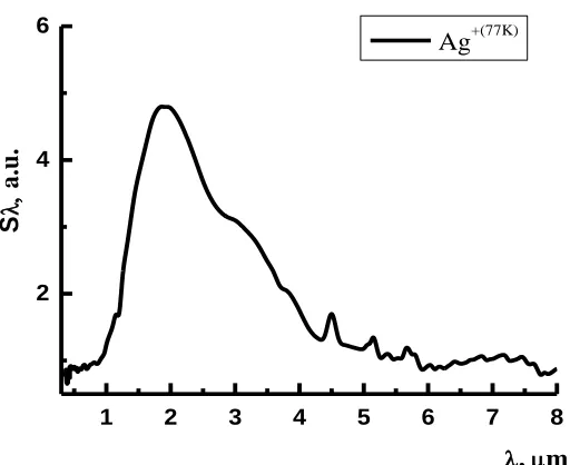
+(77K)Fig. 5 Spectral sensitivity for the system Ag2O-CdxHg1–xTe (х = 0.223).
Photosensitivity in sub-mm range was obtained at the room temperature. NEP = 2.7 * 10-8 (W Hz -1/2) and D = 3 * 109 (sm Hz 1/2W-1) were calculated for the mentioned heterostructure. The results indicate the use of this structure for manufacturing of Hg(Cd)Te photodetectors both in sub-THz and IR regions [15].
IV.CONCLUS ION
1. Using the method of silver imp lantation of the solid solution Hg1–xCdxTe (х ~ 0.223) with the next
low-temperature treat ment, the authors obtained nano -heterostructure Ag2O-Hg1–xCdxTe (x = 0.2) on surface of the samples.
2. Analog model of impedance spectroscopy was obtained using the EIS analyser. Analog model of impedance spectroscopy containing the inductance L was defined. Possible to this fact expla ined bythe presence the current transfer inhibit addit ional o xide barriers.
3. A phase shift between the current and voltage φ = 86° point out the loss mechanica l energy in the nano -materia l. So, we have appro ximation for a general p ie zoelectric transducer (actuator) operating near resonance.
4. Photosensitivity was obtained in both in sub -THz and IR regions. Therefore nano-heterostructure Ag2O-Hg1– xCdxTe (x = 0.2) can be used for manufacturing photodetectors of mult ispectral range.
ACKNOWLEDGMENT
The author e xpresses his gratitude for the participation in the experiment, and writ ing articles: R.K. Savkina2, A.B.
Smirnov3 and F.F. Sizov4. A.B. Smirnov exp ressed especially gratefu l for the measurement of spectra of
photoconductivity on the SPM-2. Sen ior scientific researcher Dept. of physical and technological proble ms of
semiconductor IR-techniques, V. Lashkaryov Institute of Semiconductor Physics, NAS of Ukra ine 2
Senior scientific researcher Dept. of physical and technological proble ms of semiconductor IR-techniques, V.
Lashkaryov Institute of Semiconductor Physics, NAS of Ukra ine 3 A.M. Professor Dept. of physical and technological
problems of se miconductor IR-techniques, V. Lashkaryov Institute of Se miconductor Physics, NAS of Ukraine 4
REFER ENC ES
[4] Jin Wei, “Au CdHgT e quantum dots for in vivo tumor-targeted,” Anal. Bioanal. Chem., vol. 403, Iss. 4, pp. 1343-1352, Feb. 2012.
[5] Marwa Abdul Muhsien, Haidar Hamed Hamdan “Preparation and Characterization of p-Ag2O/n-Si Heterojunction Devices Produced by
Rapid Thermal Oxidation” Energy Procedia., vol. 18, pp. 300–311, Dec. 2012.
[6] Sung H. Lim, Liang Feng, Jonathan W. Kemling, Christopher J. Musto and Kenneth S. Suslick, “An optoelectronic nose for the de tection of toxic gases” Nature chemistry., vol. 1, pp. 562- 567, Sept. 2009.
[7] A. B. Smirnov, O. S. Litvin, V. O. Morozhenko, R. K. Savkina, M. I. Smoliy, R. S. Udovytska and F. F. Sizov,” Role of Mechanical Stresses at Ion Implantation of CdHgT e Solid Solutions,” Ukr.J.Phys., vol. 58, Num. 9, pp. 872-880, Oct. 2013.
[8] A. B. Smirnov, A. I.Gudymenko, V. P.Kladko, A. A. Korchevyi, R. K. Savkina, F. F. Sizov and R. S. Udovitska, “Nano-scale pattern formation on the surface of HgCdT e produced by ion bombardment,” Phys. Stat. Sol. (c)., vol. 12, Iss. 8., pp. 1175–1178, Apr. 2015
[9] A. Romanyuk and P. Oelhafen, “Use of ultrasound for metal cluster engineering in ion implanted silicon oxide,”Appl. Phys. Lett., vol. 90, Iss. 1, pp. 013118, Jan. 2007.
[10] A. K. Ivanov-Shits, I. V. Murin, “Ionics of solids,” V. 1. Published in St.-Petersburg university, pp. 617, 2000. (in Russian). [11] Macdonald J. Ross, “ Impedance spectroscopy,”Annals of Biomedical Engineering, vol. 20, Iss. 3, pp. 289 -305, May 1992.
[12] C. F. Wan, J. D. Luttmer, R. S. List, and R. L. Strong, “Piezoelectric effects in HgCdT e devices,” Journal of Electronic Materials, vol. 24, Iss. 9, pp.1293-1297, Sept. 1995.
[13] F. F. Sizov, R. K. Savkina, A. B. Smirnov, R. S. Udovytska, V. P. Kladko at ell., “ Structuring effect of heteroepitaxial CdHgT e/CdZnTe systems under irradiation with silver ions,” Physics of the solid state., vol. 56, num. 11, pp. 2160-2165, Nov. 2014.
[14] A. L. Stepanov, V. A. Zhikharev, I. B. Khaibullin, “ Depth profiles of metal ions implanted in dielectrics at low energies,” Physics of the Solid State, vol. 43, Iss. 4, pp. 733-739, Apr. 2001.
[15] F. Sizov, V. Zabudsky, S. Dvoretskii, V. Petryakov, A. Golenkov, K. Andreyeva, and Z. Tsybrii, “T wo-color detector:Mercury-cadmium-telluride as a terahertz and infrared detector,” Appl. Phys. Lett., vol. 106, Num. 8, pp. 082104, March 2015.
BIOGRAPHY
R.S. Udovytska, Researcher, Dept. o f Dept. o f physical and technological proble ms of se miconductor IR -techniques, V. Lashkaryov Institute of Se miconductor Physics, NAS of Ukraine.
Date and pl ace of bir th: 22 April 1983, Dnepropetrovsk, Ukraine
Education: M . Sc . in Genera l Physics , Taras Shevchenko Kyiv University, Kyiv, Ukra ine, 2006. Institute of Semiconductor Physics of NAS of Ukra ine, Kyiv, Ukra ine, Post graduate student, 2006-2010.
Specialization: IR semiconductor detectors
Сurrent research interest: surface modification by ion imp lantation, nanostructures, semiconductor equipment
manufacturers, strain heterostructure
Honours, Awar ds, Fellowshi ps, Me mbership of Pr ofessional Societies:
1. SPIE Leadership Grant 2004 2. Travel Contingency Grant 2005