A PQ Improved High Efficiency, High Power
Operated Single-Phase Variable Input Fed Two
Switch Buck Boost Dc- Dc Converter
Harshita Saxena1, Shikha Singh2 1, 2
Dept. Of EE, Shri Ram Swaroop Memorial University, Lucknow, U.P.
Abstract: The usage of power electronic systems has expanded to new and wide application range. In recent years, the use of buck boost converters is more when compared to other type of converters. When compared with the basic converters like cuk, zeta and the two switch buck boost converter (TSBB) presents less voltage losses on the switches. The two-switch buck boost converter is suitable for wide input voltage applications. The two switch buck boost converter requires fewer passive components. In order to achieve high efficiency over the entire input voltage range, the TSBB converter operated in buck mode at high input voltage and boost mode at low input voltage. Such operation is called two mode control scheme. The objective of this paper is to propose an input voltage feed-forward (IVFF) method to reduce the influence of the input voltage disturbance on the output voltage. The TSBB converters have been extensively used in telecommunications, battery operated vehicles, etc. with wide input voltage range. So it is thus important to improve the efficiency of TSBB converter over a high input voltage range. The two mode control scheme with the IVFF compensation is then proposed for the TSBB for different operating modes has been derived.
Keywords: Input Voltage Feed-Forward, Two-Mode Control Scheme, Two-Switch Buck-Boost Converter, Power Factor
Correction
I. INTRODUCTION
The two switch buck boost converter is a simplified cascade connection of buck and boost converters.[1] Compared with basic converters, which have the ability of both voltage step-up and step-down such as inverting buck-boost, cuk, zeta and sepic converters, the TSBB converter presents lower voltage stress of the power devices, fewer passive components and positive output voltage and it has been widely used in telecommunication systems, battery-operated power supplies,[5],[6] fuel cell power systems,[7],[8] power factor correction applications,[9],[10] radio frequency amplifier power supplies,[11] all of which have wide input voltage range. The role of a DC-DC converter is very important where we need a constant DC voltage from a variable DC source like solar, fuel cells, etc. On the other hand, we can get a variable DC voltage from a fixed DC source by using DC-DC converter. There are so many types of dc-dc converters available, Buck converter- to get the reduced output voltage. Boost converter- to get the output voltage more than input. Buck-Boost- to do both the operations buck and boost. Normally, buck-boost converter consists of single switch to do both the operations buck and boost according to MATLAB simulation model of Buck Boost DC-DC converter, according to the duty cycle of the gate pulse. Single switch buck-boost converter produces an inverting output with respect to input. This is a disadvantage of this converter. To get a non-inverting output voltage the converter is designed with two switches one for buck operation and another one for boost operation. The two mode control is achieved by implementing the input feed forward method. According to the input voltage level, buck or boost switch is selected.[2],[3]
There are two active switches in the TSBB converter, which provides the possibility of obtaining various control methods for this converter. If Q1 and Q2 (switches) are switched ON and OFF simultaneously, the TSBB converter behaves the same as the single switch buck-boost converter. This control method is called one mode control scheme.[12] Q1 and Q2 can also be controlled in other manners. For example, when the input voltage is higher than the output voltage, Q2 is always kept OFF, and Q1 is controlled to regulate the output voltage, and as a result, the TSBB converter is equivalent to a buck converter, and is said to operate in buck mode.
II. LITERATUREREVIEW
Modern electronic equipment operating at varying input voltage range requires high efficiency and power factor control. Power converters provide a highly efficient means to deliver a regulated voltage from a standard power source. However, circuit trends need voltage/current requirements outside the efficient range of most classical converters and therefore new converter topologies must be developed. This literature survey gives an account of the various research works carried out in the design of converters to reduce the component stresses and the switching losses, while achieving high efficiency and improved performance.
The switched mode DC-DC converters are some of the simplest power electronic circuits which convert one level of voltage into another level by switching action. These converters have received an increasing deal of interest in many areas. This is due to their wide range applications like power supplies for personal computers, office equipments, appliance control, telecommunication equipments, automotive, aircraft, etc. [20]
In many industrial applications, it is required to convert a fixed-voltage dc source into a variable-voltage dc source. A dc-dc converter converts directly from dc to dc and is simply known as a dc converter. A dc converter can be considered as dc equivalent to an ac transformer with continuously variable turns ratio. Like transformer, it can be used to step down or step up a dc voltage source.[21] Dc converters widely used for traction motor in electric automobiles, trolley cars, marine hoists, and forklift trucks. They provide smooth acceleration control, high efficiency, and fast dynamic response. The DC-DC converter is considered as the heart of the power supply, thus it will affect the overall performance of the power supply system. The converter accepts DC and produces a controlled DC output.
A buck-boost converter provides an output voltage that may be less than or greater than the input voltage hence the name ‟
buck-boost‟; the output voltage polarity is opposite to that of the input voltage. This converter is also known as an inverting regulator. A
dc-dc switching regulator is known to be superior over a linear regulator mainly because of its better efficiency and higher current-driving capability. There are various topologies in the context of dc-dc converters the buck-boost converter are widely used. The output voltage of a dc-dc converter is controlled by operating it in the closed loop, and altering its MOSFET (switch) gate signal accordingly. It is basically governed by a switching logic, thus constituting a set of subsystems depending upon the status (on-off) of the switch. In the well known pulse width modulation (PWM) technique, the control is accomplished by varying the duty ratio of an external fixed frequency clock through one or more feedback loops, whenever any parameter varies. PI controllers are the most widely-used type of controller for industrial applications. They are structurally simple and exhibit robust performance over a wide range of operating conditions. In the absence of the complete knowledge of the process these types of controllers are the most efficient of choices.[22],[23] In compare with one-mode control scheme, two-mode control scheme can reduce the conduction loss and switching loss effectively, leading to a high efficiency over a wide input voltage range, as explained in [4]. Besides, in order to achieve automatic switching between buck and boost modes, the two-mode control scheme based on two modulation signals with one carrier or one modulation signal with two carriers was proposed in [14]. When the TSBB converter operates in continuous current boost mode, it presents a right-half-plane zero. This RHP zero limits the bandwidth of the control loop, penalizing the transient response [15]. Moreover, in the two-mode control scheme with automatic mode-switching, only one voltage regulator is used for both buck and boost modes, and it is often designed to have enough phase margin in boost mode by reducing the bandwidth of the control loop, thus the transient responses of this converter are deteriorated in the whole input voltage range, including both buck and boost modes. To improve the transient response of the TSBB converter, average current mode control [16], current-programmed mode control [17], [18], and voltage mode control with a two-mode proportional-integral derivative (PID) [19], With these control schemes mentioned earlier, the influence of the input voltage and load disturbances on the output voltage can be well reduced, but cannot be fully eliminated. For the converter in the applications with wide input voltage variation, input voltage feed-forward (IVFF) compensation is an attractive approach for improving the transient response of the converter, for it can eliminate the effect of the input voltage disturbance on the output voltage in theory.
The performance of non-inverting two-switch buck-boost converter is analysed. PI control technique is used to regulate the output voltage and it is verified that the performance of TSBB converter is better than the single switch buck-boost converter in both steady state and transient conditions. [24]Two switch buck boost converter has the advantage of reduced switching losses. Study on various controllers is need to be done and an average current mode controller which is found to be more effective is selected. High efficiency over the whole input output voltage range and improved transient response are achieved for TSBB converter.[25]
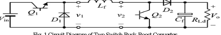
A. two Switch Buck Boost Converter
two-mode control scheme. Figure 1 shows the circuit diagram of TSBB converter. There are two active switches in the TSBB
converter, which provides the possibility of obtaining various control methods for this converter. If Q1 and Q2 are switched ON and
[image:4.612.118.497.132.193.2]OFF simultaneously, the TSBB converter behaves the same as the single switch buck-boost converter. This control method is called one mode control scheme .If Q1 and Q2 are controlled independently; it is two mode control scheme.
Fig. 1 Circuit Diagram of Two Switch Buck-Boost Converter
Modes of operation can be explained in two stages, when switch Q1 is controlled and Q2 is off and when Q1 is continuously on and Q2 is controlled to regulate the output voltage.
a. When the input voltage is higher than the output voltage, Q2 is always kept OFF, and Q1 is controlled to regulate the output voltage, and as a result, the TSBB converter is equivalent to a buck converter, and is said to operate in buck mode.
b. When the input voltage is lower than the output voltage, Q1 is always kept ON, and Q2 is controlled to regulate the output
voltage, and in this case, the TSBB converter is equivalent to a boost converter, and is said to operate in boost mode.
Compared with one-mode control scheme, two-mode control scheme can reduce the conduction loss and switching loss effectively, leading to a high efficiency over a wide input voltage range, as explained in [4]. Besides, in order to achieve automatic switching between buck and boost modes, the two-mode control scheme based on two modulation signals with one carrier signal is used. For the converter in the applications with wide input voltage variation, input voltage feed-forward (IVFF) compensation is an attractive approach for improving the transient response of the converter, for it can eliminate the effect of the input voltage disturbance on the output voltage . For one stage PFC converters, the main challenge is the availability of only one control variable to perform voltage regulation and power factor correction in a single step. As a result, in the design of the controller, a trade off needs to be considered between output voltage regulation and power factor correction. IVFF control circuit perform both voltage regulation and power factor correction. The IVFF of the buck or boost converter can be implemented in several methods.
1) Vary either the amplitude of the carrier signal or the value of the modulation signal according to the input voltage. However,
the variations of the carrier signal for the IVFF of the boost converter and the modulation signal for IVFF of the buck converter are both inversely proportional to the input voltage, which imply that the implementation of this IVFF method is complicated relatively for the TSBB converter.
2) Calculating the duty ratio. Since the duty ratio for the buck converter is inversely proportional to the input voltage results in
complicated design.
3) Deriving IVFF functions in both buck and boost modes of operation which is easy to implement.
B. Two Mode Control Scheme For Tsbb Converter
Voltage conversion ratio for TSBB converter in continuous current mode is,
In the two-mode control scheme, d1 and d2 are controlled independently. When the input voltage is higher than the output voltage,
the TSBB converter operates in buck mode, where d2 = 0 and d1 is controlled to regulate the output voltage. When the input voltage
is lower than the output voltage, the TSBB converter operates in boost mode, where d1 = 1and d2 is controlled to regulate the output
voltage. Thus, the voltage conversion of the TSBB converter is ,
III. CONCLUSIONS
automatic selection of operating modes for TSBB converter. With reasonable simplification of the IVFF function in boost mode, a general, easy implementation and effective two mode control scheme with IVFF compensation is proposed to achieve automatic selection of operating modes and the corresponding IVFF compensations for the TSBB converter. Moreover, the switching between buck and boost modes in this proposed control scheme is nearly smooth. In order to present the merits of this proposed control scheme clearly, comparisons between the two-mode control scheme with and without IVFF compensation, including the output signals of the voltage regulator and the input-to-output voltage transfer functions, are discussed.
IV. ACKNOWLEDGMENT
I would like to thank the faculties of Department of Electrical Engineering, Shri Ram Swaroop Memorial University for their encouragement and support. I would also like to express gratitude towards the institution for the laboratory and other facilities offered for the completion of the work.
REFERENCES
[1] R. W. Erickson and D. Maksimovic, Fundamentals of Power Electronics. Norwell, MA, USA: Kluwer, 2011
[2] Wei, C., C. Chen, K. Wu and I. Ko, 2012. “Design of an average-current-mode non inverting buck-boost dc-dc converter with reduced switching and conduction losses,” IEEE Trans. Power Electron., 27(12): 4934-4943.
[3] Yao, C., X. Ruan and X. Wang, 2011. “Isolated buck-boost dc/dc converters suitable for wide input-voltage range,” IEEE Trans. Power Electron.,26(9): 2599-2613.
[4] X. Ren, X. Ruan, H. Qian, M. Li, and Q. Chen, “Three-mode dual frequency two-edge modulation scheme for four-switch buck-boost converter,” IEEE Trans. Power Electron., vol. 24, no. 2, pp. 499–509, Feb.2009.
[5] Y. J. Lee, A. Khaligh, A. Chakraborty, and A. Emadi, “A compensation technique for smooth transitions in a noninverting buck-boost converter,” IEEE Trans. Power Electron., vol. 24, no. 4, pp. 1002–1016, Apr. 2009.
[6] Y. J. Lee, A. Khaligh, A. Chakraborty, and A. Emadi, “Digital combination of buck and boost converters to control a positive buck-boost converter and improve the output transients,” IEEE Trans. Power Electron., vol. 24, no. 5, pp. 1267–1279, May 2009.
[7] E. Schaltz, P. O. Rasmussen, and A. Khaligh, “Non-inverting buck-boost converter for fuel cell application,” in Proc. IEEE Annual Conf. IEEE Ind.Electron., 2008, pp. 855–860.
[8] H. Qu, Y. Zhang, Y. Yao, and L. Wei, “Analysis of buck-boost converter for fuel cell electric vehicles,” in Proc. IEEE Int. Conf. Veh. Electron. Safety, 2006, pp. 109–113.
[9] G. K. Andersen and F. Blaabjerg, “Current programmed control of a single-phase two-switch buck-boost power factor
[10] R. Morrison and M. G. Egan, “A new modulation strategy for a buckboost input ac/dc converter,” IEEE Trans. Power Electron., vol. 16, no. 1,pp. 34–45, Jan. 2001.
[11] B. Sahu and G. A. Rincon-Mora, “A high-efficiency linear RF power amplifier with a power-tracking dynamically adaptive buck-boost supply,” IEEE Trans. Microw. Theory Techniques, vol. 52, no. 1, pp. 112–120, Jan.2004
[12] H. Liao, T. Liang, L. Yang, and J. Chen, “Non-inverting buck-boost converter with interleaved technique for fuel-cell system,” IET Power Electron.,vol. 5, no. 8, pp. 1379–1388, 2012.
[13] C. Yao, X. Ruan, and X.Wang, “Isolated buck-boost dc/dc converters suitable for wide input-voltage range,” IEEE Trans. Power Electron., vol. 26,no. 9, pp. 2599–2613, Sep. 2011
[14] T. Ishii, M. Yoshida, M. Motomori, and J. I. Hara, “Buck-boost converter,”U.S. Patent 7 268 525, 2007.
[15] C. Restrepo, T. Konjedic, J. Calvente, M. Milanovic, and R. Giral, “Fast transitions between current control loops of the coupled-inductor buckboost dc-dc switching converter,” IEEE Trans. Power Electron., vol. 28, no. 8, pp. 3648–3652, Aug. 2013
[16] C. Wei, C. Chen, K. Wu, and I. Ko, “Design of an average-current-mode non-inverting buck-boost dc-dc converter with reduced switching and conduction losses,” IEEE Trans. Power Electron., vol. 27, no. 12, pp. 4934–4943, Dec. 2012
[17] J. Park, J. Fan, X.Wang, and A. Huang, “A sample-data model for double edge current programmed mode control (DECPM) in high-frequency and wide-range dc-dc converters,” IEEE Trans. Power Electron., vol. 25, no. 4, pp. 1023–1033, Apr. 2010
[18] A. A. Ahmad and A. Abrishamifar, “A simple current mode controller for two switches buck-boost converter for fuel cells,” in Proc. IEEE Elect. Power Conf., 2007, pp. 363–366
[19] R. Paul, L. Sankey, L. Corradini, Z. Popovic, and D.Maksimovic, “Power management of wideband code division multiple access RF power amplifiers with antenna mismatch,” IEEE Trans. Power Electron., vol. 25, no. 4, pp. 981–991, Apr. 2010
[20] B. Sahu and G. A. Rincon-Mora, “A low voltage, dynamic, noninverting, synchronous buck-boost converter for portable applications,” IEEE Trans. Power Electron., vol. 19, no. 2, pp. 443–452, Mar. 2004
[21] C. Restrepo, J. Calvente, A. Cid-Pastor, A. E. Aroudi, and R. Giral, “A noninverting buck-boost dc-dc switching converter with high efficiency and wide bandwidth,” IEEE Trans. Power Electron., vol. 26, no. 9, pp. 2490–2503, Sep. 2011
[22] N. Mohan, T. M. Undeland and W. P. Robbins, “Power Electronics: Converters, Applications and Design,” John Wiley and Sons Inc, USA,1995
[23] Y. J. Lee, A. Khaligh, A. Chakraborty, and A. Emadi, “Digital combination of buck and boost converters to control a positive buck-boost converter and improve the output transients,” IEEE Trans. Power Electron., vol. 24, no. 5, pp. 1267–1279, May 2009.
[24] E. Schaltz, P. O. Rasmussen, and A. Khaligh, “Non-inverting buck-boost converter for fuel cell application,” in Proc. IEEE Annual Conf. IEEE Ind. Electron., 2008, pp. 855–860.