N A N O E X P R E S S
Open Access
InAs/GaAs Quantum Dot Dual-Mode
Distributed Feedback Laser Towards Large
Tuning Range Continuous-Wave Terahertz
Application
Qi-zhu Li
1,5, Yuan-qing Huang
1,2, Ji-qiang Ning
3, Cheng Jiang
1, Xu Wang
1, Hong-mei Chen
1, Xiao Li
1,
Rui-ying Zhang
1, Kai Zhang
4, Jia-hua Min
5, Yong Peng
2*and Zi-yang Zhang
1*Abstract
In this paper, a laterally coupled distributed feedback (LC-DFB) laser based on modulation p-doped multiple InAs/ GaAs quantum dot (QD) structures has been fabricated. The device exhibits a high side-mode suppression ratio (SMSR) of > 47 dB and a high thermal stability of dλ/dT = 0.092 nm/K under continuous-wave (CW) operation, which is mainly attributed to the high material gain prepared by modulation p-doping and rapid thermal annealing (RTA) process, and the significantly reduced waveguide losses by shallow-etched gratings and its close proximity to the laser ridge feature in the LC-DFB laser. With this superior performance of the DFB laser, the wide tunable dual-wavelength lasing operation has been obtained by delicately defining different periods for the grating structures on the two sides of the laser ridge or combining the reduced laser cavity length. The wavelength spacing between the two lasing modes can be flexibly tuned in a very wide range from 0.5 to 73.4 nm, corresponding to the frequency difference from 0.10 to 14 THz, which is the largest tuning range by the utilization of single device and hence providing a new opportunity towards the generation of CW THz radiation.
Keywords:Quantum well, wire, and dot devices, Distributed feedback, Terahertz imaging, Lasers, Semiconductor lasers, Optoelectronics
Background
Distributed feedback (DFB) lasers are technologically significant for their wide range of applications in long-distance fiber optical communication and terahertz (THz) radiation due to their narrow emission spectrum and stabilized emission wavelength [1–3]. Great efforts and various attempts have been made in the past decade to pursue high-performance DFB lasers, and quantum dot (QD)-based DFB lasers have exhibited advantageous
performances such as low threshold current, high quantum efficiency, broadband wavelength tuning range, and high-temperature stability over commercial quantum well-based devices [4–6]. The modulation p-doping in quantum dot laser structures has been dem-onstrated as an effective method to further improve the QD laser performance including the temperature stabil-ity [7] and high-speed modulation characteristics [8] due to the significantly enhanced ground state (GS) gain. Moreover, it has also been found that rapid thermal an-nealing (RTA) is another efficient way to optimize the material quality and optical properties of the QD assem-blies, owing to the reduction of point defects and dislo-cations that are produced during the epitaxy growth. The conventional fabrication process of a DFB laser usu-ally requires two steps of high-quality epitaxial growth [9]. Stubenrauch et al. reported the fabrication of a 1.3-μm QD DFB laser which shows high static and * Correspondence:[email protected];[email protected]
Qi-zhu Li and Yuan-qing Huang contributed equally to this work and should be considered co-first authors.
2Lab of Magnetism and Magnetic Materials of the Ministry of Education,
School of Physical Sciences and Technology, Electron Microscopy Centre of Lanzhou University, Lanzhou University, Lanzhou 730000, People’s Republic of China
1Key Laboratory of Nanodevices and Applications, Suzhou Institute of
Nano-Tech and Nano-Bionics, Chinese Academy of Sciences, Suzhou 215123, People’s Republic of China
Full list of author information is available at the end of the article
dynamic performance; however, after the fabrication of a Bragg grating structure and epitaxy growth of bottom cladding layer and active region, a metalorganic vapor chemical deposition (MOCVD) epitaxial re-growth step is required to complete the whole laser structure leading to many complex and uncertain factors [1]. To avoid the re-growth process, Goshima et al. proposed a QD-based laterally coupled distributed feedback (LC-DFB) laser structure which was realized by deeply etching the grat-ing vertically into the ridge waveguide, but low slope ef-ficiencies below 0.03 W/A and small side-mode suppression ratio (SMSR) of 20 dB were observed due to large waveguide losses [10]. The waveguide losses are mainly from the deep etching process, by which the high-quality and uniform grating structure is very diffi-cult to realize due to the technical issues of high aspect ratio (normally 20:1) requirement in either dry etching or wet etching process [11]. So, in order to realize a super high-performance DFB laser, it is necessary to trace a way to combine the optimized QD active region with improved device waveguide structure together.
Terahertz (THz) frequency radiation sources have attracted considerable attention for their prosperous med-ical, agriculture, environment, and security applications [12,
13] and that frequency-tunable continuous-wave (CW) op-eration of the THz radiation source with compact size and low cost is especially desired. Recently, various semicon-ductor dual-mode lasers have been studied for the aim of developing an optical beat source for THz photomixing. Broad frequency tuning has been demonstrated by using external-cavity lasers which emit two lines of different wavelengths simultaneously [14,15]. However, the mechan-ical moving parts in the external-cavity laser system are nei-ther convenience nor stable for wavelength tuning. CW THz signals can also be generated by using two independ-ent DFB laser beams of slightly differindepend-ent frequencies. This technique has emerged as an excellent choice to generate THz radiation benefitting from the very narrow emission spectrum and stabilized emission wavelength of DFB laser diodes [3,16–18]. Besides those reported configurations for THz photomixing, the simultaneous emission of two tun-able laser lines from a single DFB laser cavity is very appeal-ing due to its compactness, high-temperature stability, and high spectral quality [3,19].
In this work, the multiple InAs/GaAs QD laser struc-tures were grown by molecular-beam epitaxy (MBE), and p-type modulation doping was applied to the QD active region. After epitaxy growth, the QD samples were treated by a post-growth annealing process. To avoid the overgrowth step and reduce the aspect ratio in grating etching, the LC-DFB laser was fabricated with shallow-etched gratings. The shallow-etched LC-DFB la-sers based on the p-doped QDs exhibit a high differen-tial efficiency of 0.2 W/A, a large SMSR of 47 dB, and a
high thermal stability dλ/dT of 0.092 nm/K. In addition, dual-mode lasing was successfully obtained with the LC-DFB lasers by fabricating two sets of gratings of dif-ferent periods, and the lasing wavelengths can be simply manipulated by delicately modifying the grating periods, which enable a large range tuning of the frequency dif-ference of the two lasing modes from 0.10 to 14 THz. Our work demonstrates the promise applications of QD-based LC-DFB lasers for long-distance fiber-optic communication and CW THz radiation sources.
Methods
Preparation and Characterization of Materials
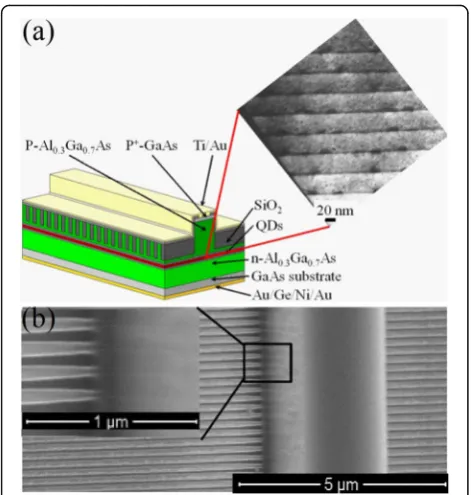
The InAs/GaAs QD laser structures were grown on Si-doped GaAs (100) substrates by a MBE system. The ac-tive region of the laser structure is eight stacks of QD layer separated by GaAs barriers of 33 nm in thickness. Each QD layer comprises 2.7 ML InAs covered with a 6-nm-thick InGaAs strain-reducing layer. And the whole active region is sandwiched by the cladding layers of the lower ~ 2800 nm n-Al0.3Ga0.7As and the upper ~ 1800 nm p-Al0.3Ga0.7As. The deposition of the InAs at a growth temperature of 510 °C and a growth rate of 0.01 ML/s. The modulation p-doping with Be was conducted in a 6-nm layer located in the GaAs spacer layer 10 nm be-neath each QD layer, and the doping concentration was controlled to be 25 acceptors per dot. The cross-sectional transmission electron microscopy (TEM) image of the InGa/GaAs QD layers is shown in Fig.1a. The density of InAs/GaAs QDs is determined to be 4 × 1010 cm−2 by atomic force microscope measurement. The RTA treat-ment was performed in a N2ambient at the temperature of 700 °C for 45 s. The QD samples were protected by a GaAs proximity cap during the annealing process.
Referring to the coupling principle of LC-DFB, it is well known that the proximity of the gratings to the ridge is a key factor that greatly influences the laser per-formance [20]. In the fabrication process, after the ridge waveguide is first defined, the sample for electron-beam lithography (EBL) has a height difference with respect to the waveguide, and the photoresist will stack aside the sidewall during EBL, which makes it difficult to make the formation of grating adjacent to the ridge. In order to solve the problem of the nonuniform photoresist coating and to form a high-quality grating patterned by EBL, the thickness of polymethylmethacrylate (PMMA) resist was carefully selected to be as thin as 75 nm, which is opti-mized to enable the grating quality to reach their equilib-rium points. The LC-DFB laser was fabricated through the following procedures. First, a 75-nm SiO2layer was deposited on top of the epitaxy structure by using plasma-enhanced chemical vapor deposition (PECVD), which acts as the etching protecting layer for the shallow etching of gratings. The ridge waveguide structure was patterned using optical lithography and etched to a depth of around 1.75 μm with the technique of inductively coupled plasma (ICP) with a gas mixture of Cl2and BCl3. With the waveguide structure having been defined, the upper p-side AlGaAs cladding layer was further etched by wet etching which was stopped at~ 280 nm above the QD
active regions. After that, the sample was spin-coated with PMMA resist (molecular weight of 950 K and thickness of 75 nm) and baked for 90 s at 180 °C. The first-order grat-ing was defined alongside the ridge waveguide by EBL, and then the resist image was transferred into the AlGaAs by ICP dry etching. The etch rates of PMMA resist and AlGaAs were approximately 5 nm/s and 10 nm/s, respect-ively. A scanning electron microscopy (SEM) image of the fabricated LC-DFB structure is shown in Fig.1b. Benefit-ting from the careful choice of the EBL exposure dose and the greatly alleviated photoresist stacking due to the thin resist, the gratings are tightly linked to the laser ridge waveguide, as revealed by the inset of Fig.1b. The etching depth of grating is 135 nm, and the grating period is 194 nm. To achieve a precisely and widely tuned dual-wavelength lasing, two different Bragg periods were fabricated for lateral gratings at the two sides of the ridge waveguide. The Ohmic contact layer on the ridge wave-guide was completely protected by the 75-nm-thick SiO2 protecting layer to ensure Ohmic contact surviving during the ICP etching process. The shallow-etched grating was controlled to be 150 nm above the QD active range to form a good coupling with light. For the aim of insulation and planarization, another layer of SiO2was deposited on the sample with PECVD after etching the gratings. Finally, reactive ion etching (RIE) dry etching was employed to open a contact window in SiO2. Ti/Au and Au/Ge/Ni/Au were then deposited to form the top and bottom Ohmic contacts, respectively. The substrates were thinned down to around 80μm to minimize the self-heating effect. The laser cavities of 1 and 0.45 mm long were fabricated, and the emitting facets were not coated. The laser bars were mounted with the p-side up on a copper heat sink, and all the measurements were performed under CW operation.
Results and Discussion
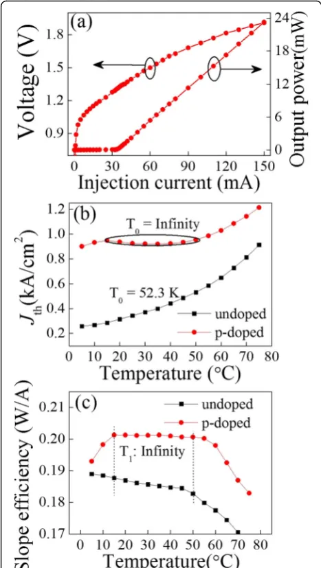
Figure2ashows a typical power–current–voltage (P–I–V) characteristic of the as-fabricated LC-DFB laser based on a multiple modulation p-doped QD structure. The laser shows an obvious high slope efficiency of 0.20 W/A and a low threshold of 33 mA, which reveals the high material quality and high optical gain of the QD structure. The threshold current density and slope efficiency with respect to the temperature for an undoped and a p-doped QD LC-DFB lasers are presented in Fig. 2b, c, respectively. The characteristic temperature for the threshold current density (T0) of 52.3 K is calculated for the undoped QD LC-DFB laser as seen in Fig.2b, while theT0for p-doped QD LC-DFB laser has a significant increase, especially in the temperature range from 15 to 50 °C, in which an infin-ite T0 is observed. Moreover, in this temperature range, the slope efficiency almost shows no degradation (2.6% degradation for the undoped QD LC-DFB laser), indicat-ing an infinite characteristic temperature for the slope
[image:3.595.56.292.86.334.2]efficiency (T1) for p-doped LC-DFB laser as well. The big difference of bothT0 and T1 between the undoped and p-doped LC-DFB lasers is mainly attributed to the effects induced by the built-in excess holes due to the modulation p-doping which can significantly inhibit holes’ thermal broadening in the closely spaced energy levels [21, 22]. Based on the above results, the p-doped QD LC-DFB laser was selected for the further lasing spectra characterization.
The inset of Fig.3shows an emission spectrum of the p-doped LC-DFB laser of 1 mm in cavity length mea-sured under I= 2Ith injection level at room temperature (RT), and a single longitudinal mode lasing at 1292.4 nm with a very large SMSR of 47 dB can be observed.
Figure3shows the emission wavelength as a function of the operation temperature of the p-doped LC-DFB laser, which reveals a variation rate of only 0.092 nm/K. The high-temperature stability of the lasing wavelength is in good accordance with the temperature coefficient of the refractive index, which is about five times lower than that of the material gain shift.
Recently, Goshima et al. [10] reported a 1.3-μm InAs/ GaAs QD LC-DFB laser fabricated by deep gratings vertically etched into the ridge waveguide structure, and a low slope efficiencies below 0.03 W/A and a small SMSR of 20 dB were observed, which are mainly due to the large waveguide losses caused by the deep etching process. With a shallow-etched grating struc-ture, Briggs et al. [23] have successfully fabricated GaSb-based LC-DFB lasers with a larger SMSR of 25 dB. But further improvement was limited by the lower coupling coefficient due to the large distance be-tween the gratings and the ridge waveguide, which is crucial for the performance of a LC-DFB laser. In our work, the narrow ridge waveguide and the grating structures were fabricated separately, resulting in a very sharp and smooth sidewall of the ridge waveguide and therefore little waveguide loss. The shallow etching method for the grating fabrication employed in our ex-periments can sharply reduce the aspect ratio of the etched gratings and allow the making of the high-qual-ity first-order grating structure which ensures good coupling with light. By carefully controlling the thick-ness of the PMMA resist and the EBL lithography parameters, the stacking phenomena of photoresist aside the sidewall of ridges were effectively alleviated, which leads to the formation of gratings tightly adjacent to the laser ridge waveguide. In addition, the high dot density of ~ 4.3 × 10¹⁰
cm−2obtained by optimizing the
Fig. 2P–I–V and temperature dependence characteristic of the LC-DFB laser.aP–I–V characteristic of the p-doped LC-DFB laser at RT.b
Temperature dependences of threshold current density for undoped and p-doped LC-DFB lasers.cTemperature dependences of slope efficiency for undoped and p-doped LC-DFB lasers
[image:4.595.305.538.86.271.2] [image:4.595.56.290.88.502.2]MBE epitaxy growth parameters and the high gain of the QD assemblies realized by the modulation p-doping and the post-growth annealing treatment may account for the large 47 dB SMSR of our LC-DFB laser.
Besides the widespread applications already demon-strated in long-distance optical transmission and wave-length division multiplex (WDM) systems due to the superior features of the narrow emission spectrum and high thermal stability, the LC-DFB lasers have also dem-onstrated advantages for generating CW THz radiation. Compared with the traditional method to create THz ra-diation by using two independent diode lasers [24–26], LC-DFB lasers with simultaneous emission of two modes are very attractive for fabricating THz radiation sources due to the cost-effectiveness, compactness, high stability, and high spectral quality. In contrast to quantum well (QW) lasers, QD-based emitters are well suited for broadband tunable sources owing to two unique features of QD structures. Firstly, the nature of low density of states leads to the easy saturation of the GS levels, resulting in the further population of the excited states (ES). Secondly, the dot size variation can be utilized to extend the tuning range, due to the fact that the wide size distribution of the self-assembled QD ensemble leads to a wide spectrum of light emission governed by the quantum size effect.
The LC-DFB structure comprised of lateral gratings fab-ricated independently allows high flexibility in defining the designed Bragg wavelength. Dual-wavelength lasing can be achieved by fabricating two sets of gratings of dif-ferent Bragg periods 1and 2which enable two differ-ent wavelengths λ1 and λ2. The method reported here involves defining two different grating periods for each side of the gratings. The dual-wavelength lasing measure-ments were carried out under CW conditions. Stable dual-wavelength lasing, with SMSR around 40 dB, was ob-served. As illustrated in Fig.4a, the dark cyan, blue, red, and black lines exhibit lasing spectra with two different lasing wavelengths. For a 1-mm LC-DFB laser with grating period difference 1− 2= 0.10 nm, the two lasing wavelengths are 1292.40 and 1292.90 nm, respectively, yielding a wavelength spacing of 0.50 nm corresponding to the frequency difference of ~ 0.10 THz. By tuning the grating period difference to 0.64 nm, the dual-wavelength spacing can be extended to 4.1 nm which corresponds to a beating frequency of 0.74 THz.
To get a larger tuning range of the dual-mode lasing, the cavity length of LC-DFB lasers was carefully short-ened to 450 μm, which results in the simultaneous GS and ES lasing due to the effect of GS gain saturation and increased population of the ES. The LC-DFB laser struc-ture consists of two different Bragg periods of 182 and 194 nm, respectively, which is similar to what was de-scribed in previous reports [27,28]. As shown in Fig.4b,
the two longitudinal modes exhibit a large wavelength separation of 73.4 nm, corresponding to the frequency difference of 14 THz. By implementing two different period gratings laterally to a ridge waveguide and short-ening the cavity length delicately to allow ES lasing, the InAs/GaAs QD-based laser diodes could emit dual las-ing lines of very wide tunable wavelength spaclas-ing from 0.5 to 73.4 nm corresponding to 0.10–14 THz frequency difference. Compared with other types of proposed schemes of THz photomixing based on two separate lasers, our device offers the advantages of simple struc-ture, compact size, low fabrication cost, and a very wide tuning range.
Conclusions
A 1.3-μm QD LC-DFB laser with shallow-etched grat-ings has been fabricated, in which the complexity of overgrowth and the difficulties of deep-etching processes in general fabrication process of DFB laser are success-fully avoided. Benefitting from the high material gain of
[image:5.595.307.539.87.424.2]QD samples prepared with modulation p-doping, RTA treatment, and optimized LC-DFB laser waveguide structure, the device exhibits a large SMSR of 47 dB and a high thermal stability dλ/dT of 0.092 nm/K. By the means of defining two different periods to the gratings at each side of the narrow ridge waveguide or shortening the laser cavity length, two lasing lines can be obtained simultaneously and the spacing between the two lasing wavelengths can be flexibly and largely tuned, which can be modified from 0.5 to 73.4 nm, corresponding to the frequency difference from 0.10 to 14 THz. It is noteworthy that this wide tuning range is realized in a single laser device, which has not been reported so far. These results demonstrate the promising application of LC-DFB lasers for generating CW THZ radiation.
Abbreviations
CW:Continuous-wave; DFB: Distributed feedback; EBL: Electron-beam lithography; ES: Excited states; GS: Ground state; ICP: Inductively coupled plasma; LC-DFB: Laterally coupled distributed feedback; MOCVD: Metalorganic vapor chemical deposition; PECVD: Plasma-enhanced chemical vapor deposition; P–I–V: Power–current–voltage; PMMA: Polymethylmethacrylate; QD: Quantum dot; QW: Quantum well; RT: Room temperature; RTA: Rapid thermal annealing; SEM: Scanning electron microscopy; SMSR: Side-mode suppression ratio; TEM: Transmission electron microscopy; WDM: Wavelength division multiplex
Acknowledgements
We would like to acknowledge the financial support from the open project of Key Laboratory of Nanodevices and Applications of Suzhou Institute of Nano-Tech and Nano-Bionics (Grant no. 16ZS02) and the Thousand Youth Talents Plan.
Funding
This work is supported by the National Natural Science Foundation of China (No. 61575215 and 61674166) and the Key Research and Development Plan of the Ministry of Science and Technology (2016YFB0402303).
Availability of Data and Materials
The datasets generated and/or analyzed during the current study are available from the corresponding author on reasonable request.
Authors’Contributions
ZYZ proposed and guided the overall project. QZL and YQH performed the experiments. QZL and YQH collected and analyzed the literature and wrote the manuscript. All authors read and approved the final manuscript.
Authors’Information
QZL (student) and JHM (professor) are from School of Materials Science & Engineering, Shanghai University. YQH (student) and YP (professor) are from School of Physical Sciences and Technology, Electron Microscopy Centre, Lanzhou University; Lab of Magnetism and Magnetic Materials of the Ministry of Education, Lanzhou University. QZL (student) and YQH (student) also work at the Key Lab of Nanodevices and Applications, Suzhou Institute of Nano-Tech and Nano-Bionics, Chinese Academy of Sciences. CJ (student), XL (student), XW (postdoctoral researcher), HMC (assistant researcher), RYZ (associate professor), and ZYZ (professor) are from Key Lab of Nanodevices and Applications, Suzhou Institute of Nano-Tech and Nano-Bionics, Chinese Academy of Sciences. JQN (professor) is from Vacuum Interconnected Nanotech Workstation, Suzhou Institute of Nano-Tech and Nano-Bionics, Chinese Academy of Sciences. KZ (professor) is from i-Lab, Suzhou Institute of Nano-Tech and Nano-Bionics, Chinese Academy of Sciences.
Competing Interests
The authors declare that they have no competing interests.
Publisher’s Note
Springer Nature remains neutral with regard to jurisdictional claims in published maps and institutional affiliations.
Author details
1Key Laboratory of Nanodevices and Applications, Suzhou Institute of
Nano-Tech and Nano-Bionics, Chinese Academy of Sciences, Suzhou 215123, People’s Republic of China.2Lab of Magnetism and Magnetic Materials of the Ministry of Education, School of Physical Sciences and Technology, Electron Microscopy Centre of Lanzhou University, Lanzhou University, Lanzhou 730000, People’s Republic of China.3Vacuum Interconnected
Nanotech Workstation, Suzhou Institute of Nano-Tech and Nano-Bionics, Chinese Academy of Sciences, Suzhou 215123, People’s Republic of China.
4i-Lab, Suzhou Institute of Nano-Tech and Nano-Bionics, Chinese Academy of
Sciences, Suzhou 215123, People’s Republic of China.5School of Materials
Science and Engineering, Shanghai University, 200444 Shanghai, People’s Republic of China.
Received: 3 August 2018 Accepted: 20 August 2018
References
1. Stubenrauch M, Stracke G, ArsenijevićD, Strittmatter A, Bimberg D (2014) 15 Gb/s index-coupled distributed-feedback lasers based on 1.3μm InGaAs quantum dots. Appl Phys Lett 105(1):011103
2. Takada K, Tanaka Y, Matsumoto T, Ekawa M, Song H, Nakata Y et al (2011) Wide-temperature-range 10.3 Gbit/s operations of 1.3μm high-density quantum-dot DFB lasers. Electron Lett 47(3):206–208
3. Klehr A, Fricke J, Knauer A, Erbert G, Walther M, Wilk R et al (2008) High-power monolithic two-mode DFB laser diodes for the generation of THz radiation. IEEE J Sel Top Quantum Electron 14(2):289–294
4. Chen SM, Li W, Wu J, Jiang Q, Tang MC, Shutts S et al (2016) Electrically pumped continuous-wave III-V quantum dot lasers on silicon. Nat Photonics 10(5):307 5. Wu J, Chen SM, Seeds A, Liu HY (2015) Quantum dot optoelectronic
devices: lasers, photodetectors and solar cells. J Physics D Appl Phys 48(36):363001
6. Zhang ZY, Wang ZG, Xu B, Jin P, Sun ZZ, Liu F (2004) High-performance quantum-dot superluminescent diodes. IEEE Photon Technol Lett 16(1): 27–29
7. Shchekin OB, Deppe DG (2002) 1.3μm InAs quantum dot laser with T0= 161 K
from 0 to 80 °C. Appl Phys Lett 80(18):3277–3279
8. Shchekin OB, Deppe DG (2002) The role of p-type doping and the density of states on the modulation response of quantum dot lasers. Appl Phys Lett 80(15):2758–2760
9. Soda H, Kotaki Y, Sudo H, Ishikawa H, Yamakoshi S, Imai H (1987) Stability in single longitudinal mode operation in GaInAsP/InP phase-adjusted DFB lasers. IEEE J Quantum Electron 23(6):804–814
10. Goshima K, Tsuda N, Yamada J, Sugaya T, Komori K, Amano T (2013) 1.3-μm quantum dot distributed feedback laser with half-etched mesa vertical grating fabricated by Cl2dry etching. Jpn J Appl Phys 52(6S):06GE3
11. Li J, Cheng J (2013) Laterally-coupled distributed feedback laser with first-order gratings by interference lithography. Electron Lett 49(12):764–766 12. Tonouchi M (2007) Cutting-edge terahertz technology. Nat Photonics 1(2):97–105 13. Hosako I, Sekine N, Patrashin M, Saito S, Fukunaga K, Kasai Y et al (2007) At
the dawn of a new era in terahertz technology. Proc IEEE 95(8):1611–1623 14. Hoffmann S, Hofmann M, Kira M, Koch S (2005) Two-colour diode lasers for
generation of THz radiation. Semicond Sci Technol 20(7):S205
15. Pajarola S, Guekos G, Mork J (1996) Optical generation of millimeter-waves using a dual-polarization emission external cavity diode laser. IEEE Photon Technol Lett 8(1):157–159
16. Wilk R, Klehr A, Mikulics M, Hasek T, Walther M, Koch M (2007) Terahertz generation with 1064nm DFB laser diode. Electron Lett 43(2):108–110 17. Gregory I, Tribe W, Cole B, Evans M, Linfield E, Davies A et al (2004)
Resonant dipole antennas for continuous-wave terahertz photomixers. Appl Phys Lett 85(9):1622–1624
18. Kleine-Ostmann T, Knobloch P, Koch M, Hoffmann S, Breede M, Hofmann M et al (2001) Continuous-wave THz imaging. Electron Lett 37(24):1461–1463 19. Pozzi F, De La Rue RM, Sorel M (2006) Dual-wavelength InAlGaAs-InP
20. Yang C-A, Zhang Y, Liao Y-P, Xing J-L, Wei S-H, Zhang L-C et al (2015) 2-μm single longitudinal mode GaSb-based laterally coupled distributed feedback laser with regrowth-free shallow-etched gratings by interference lithography. Chin Phys B 25(2):024204
21. Li QZ, Wang X, Zhang ZC, Chen HM, Huang YQ, Hou CC et al (2018) Development of modulation p-doped 1310 nm InAs/GaAs quantum dot laser materials and ultrashort cavity Fabry-Perot and distributed-feedback laser diodes. Acs Photon 5(3):1084–1093
22. Zhang ZY, Hogg RA, Lv XQ, Wang ZG (2010) Self-assembled quantum-dot superluminescent light-emitting diodes. Adv Opt Photon 2(2):201–228 23. Briggs RM, Frez C, Bagheri M, Borgentun CE, Gupta JA, Witinski MF et al
(2013) Single-mode 2.65μm InGaAsSb/AlInGaAsSb laterally coupled distributed-feedback diode lasers for atmospheric gas detection. Opt Express 21(1):1317–1323
24. Brown ER, Smith FW, Mcintosh KA (1993) Coherent millimeter-wave generation by heterodyne conversion in low-temperature-grown GaAs photoconductors. J Appl Phys 73(3):1480–1484
25. Matsuura S, Tani M, Sakai K (1997) Generation of coherent terahertz radiation by photomixing in dipole photoconductive antennas. Appl Phys Lett 70(5): 559–561
26. Walton C, Bordonalli AC, Seeds AJ (1998) High-performance heterodyne optical injection phase-lock loop using wide linewidth semiconductor lasers. IEEE Photon Technol Lett 10(3):427–429
27. Grillot F, Naderi N, Lin CY, Yang K, Gin A, Shirkhorshidian A, et al (2010) Two-color quantum-dot DFB laser for terahertz applications. Photonics Society, 23rd Annual Meeting of the IEEE