N A N O E X P R E S S
Open Access
Bendability optimization of flexible optical
nanoelectronics via neutral axis engineering
Sangmin Lee
1†, Jang-Yeon Kwon
2†, Daesung Yoon
3, Handong Cho
1, Jinho You
3, Yong Tae Kang
3, Dukhyun Choi
3*and Woonbong Hwang
1*Abstract
The enhancement of bendability of flexible nanoelectronics is critically important to realize future portable and wearable nanoelectronics for personal and military purposes. Because there is an enormous variety of materials and structures that are used for flexible nanoelectronic devices, a governing design rule for optimizing the bendability of these nanodevices is required. In this article, we suggest a design rule to optimize the bendability of flexible nanoelectronics through neutral axis (NA) engineering. In flexible optical nanoelectronics, transparent electrodes such as indium tin oxide (ITO) are usually the most fragile under an external load because of their brittleness. Therefore, we representatively focus on the
bendability of ITO which has been widely used as transparent electrodes, and the NA is controlled by employing a buffer layer on the ITO layer. First, we independently investigate the effect of the thickness and elastic modulus of a buffer layer on the bendability of an ITO film. Then, we develop a design rule for the bendability optimization of flexible optical nanoelectronics. Because NA is determined by considering both the thickness and elastic modulus of a buffer layer, the design rule is conceived to be applicable regardless of the material and thickness that are used for the buffer layer. Finally, our design rule is applied to optimize the bendability of an organic solar cell, which allows the bending radius to reach about 1 mm. Our design rule is thus expected to provide a great strategy to enhance the bending performance of a variety of flexible nanoelectronics.
Keywords:Flexible optical nanoelectronics, Bendability optimization, Neutral axis engineering, Buffer layer
Background
There has been rapid development in the field of flexible optical nanoelectronics such as organic solar cells (OSCs) and organic light-emitting diodes for future portable and wearable electronic nanodevices, which have potential personal and military applications [1-10]. These optical nanodevices basically require an optically transparent win-dow to absorb or emit light. Indium tin oxide (ITO) thin films have been widely used as transparent electrodes for such optical nanoelectronics because of their high visible transparency, chemical stability, and excellent adhesion to a substrate [11-13]. However, despite its advantages, ITO
is still difficult to apply to flexible optical nanodevices without damaging the electronic functionality under an external bending load because of its brittleness. Research-ers are thus trying to find substitutes for ITO such as car-bon nanotube, graphene, and aluminum-doped zinc oxide (AZO) [10,12-14]. However, with these alternatives, it is still difficult not only to successfully achieve a high-quality and low-cost production that is as good as ITO with high transparency (higher than 90 %) and low electric resist-ance (less than 10Ω), but also to successfully increase bendability due to their brittleness which is common with ITO. Thus, it is critically necessary to develop innovative ideas and solutions to enhance mechanical stability of ITO under external bending loads.
To improve the bendability of flexible nanoelectronics, a buffer layer has been adopted [3,6,9,15]. Researchers have reported that the mechanical bendability of electronic nanodevices can be increased by using a buffer layer above or below the ITO layer. However, they did not suggest an optimized design rule that considers both the thickness * Correspondence:[email protected];[email protected]
†Equal contributors
1
Department of Mechanical Engineering, Pohang University of Science and Technology, San 31, Hyoja, Namgu, Pohang, Gyungbuk 790-784, Republic of Korea
3Department of Mechanical Engineering, College of Engineering, Kyung Hee
University, 1 Seocheon-dong, Giheung-gu, Yongin-si 446-701, Republic of Korea
Full list of author information is available at the end of the article
and elastic modulus of the buffer material. Because vari-ous buffer layers could be used to increase the thermal, chemical, and mechanical stabilities of flexible electronic nanodevices, a governing design rule is crucially needed to optimize the bendability of these flexible nanodevices re-gardless of the buffer layers that are chosen. In this article, we report a design rule for the bendability optimization of flexible optical nanoelectronics through controlling the neutral axis (NA). If we place the fragile layer such as ITO in a nanodevice at the NA position, the bending stress and strain in the layer are greatly reduced, thus enhancing the bendability of the device. Therefore, we first investigate the behavior of the NA position and the effect on the de-vice bendability by independently considering the elastic modulus and thickness of a buffer layer on the ITO. Be-cause the elastic modulus and thickness of a buffer layer influenced each other when determining the NA, we should consider these parameters together. Therefore, we develop a design rule for the bendability optimization of flexible electronics by controlling the NA position, consid-ering both the thickness and elastic modulus of the buffer layer. Finally, our design rule to optimize the bendability of flexible devices is applied to an inverted OSC with an ITO optical window. We believe that our design rule based on NA engineering will provide a great advantage to improve the bendability of flexible nanoelectronics.
Methods
[image:2.595.58.291.496.663.2]Bending theory
Figure 1 shows a cross-sectional illustration of the stress distribution of an ITO film by controlling NA. The
position of the NA is determined from the condition that the resultant axial force acting on the cross section is zero:
Z
A
σAdA¼0 ð1Þ
whereσis the longitudinal stress anddAis the element of cross-sectional area. The strain (E) curvature relation in pure bending is
E¼ yρ¼ κy ð2Þ
whereyis the distance from the NA,ρis the bending ra-dius, and κ is the curvature. The most common stress– strain relationship encountered in engineering is the equa-tion for a linearly elastic material. For such materials, we substitute Hooke's law for uniaxial stress into Equation 2 and obtain
σ¼EE¼ Eκy ð3Þ
In this equation, the normal stresses acting on the cross section are proportional to the distance,y, from the NA at a given κ. Thus, it is important to locate the most fragile material at the NA position to minimize the stress applied to the material. As shown in Figure 1a,b, when there are homogeneous films with a symmetric cross section, such as ITO and a substrate, we compared the maximum bending stresses of ITO films without and with a buffer layer. Based on Equation 3, the maximum bending stress of the ITO with a buffer layer can be significantly decreased more than that of the ITO without a buffer layer becausey2<<y1, as
shown in Figure 1c,d. In other words, by adopting a buffer layer, a fragile layer such as ITO can be located at the NA position and the bending stress acting on the fragile layer can be greatly reduced, thus leading to flexible nanoelectro-nics with high bendability.
Results and discussion
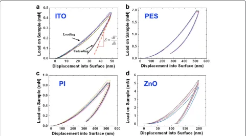
To investigate the bendability of a nanodevice according to the NA position, the elastic properties for each mater-ial should be determined. The elastic modulus of thin layers can be measured by using standard nano-indentation techniques. These techniques depend on the fact that the displacements recovered during unloading are largely elastic, which allows the Oliver and Pharr method to be used to determine the modulus from an analysis of indentation load–displacement data [16-19]. The load (P) and displacement (h) are measured directly from the indentation load–displacement curve, as shown in Figure 2a, and the contact stiffness (S) is determined by measuring the unloading slope at peak load. If the values are determined, we can obtain the elastic modu-lus for each material by using the analysis procedure of the Oliver and Pharr method [16]. Four specimens, Figure 1Scheme for NA positions of a flexible film including a
including ITO, polyethersulfone (PES), polyimide (PI), and zinc oxide (ZnO), were prepared as listed in Table 1, and nano-indentation tests for each material were per-formed under displacement control with maximum dis-placements from 50 to 500 nm using an MTS nanoindenter XP system with a Berkovich diamond in-denter (Eden Prairie, MN, USA). The tests were con-ducted at least 10 times for each specimen. Figure 2 shows the load-indentation data for a depth-sensing in-dentation experiment. The measured elastic moduli for each material are shown in Table 1, and these values are similar to the previous results [6,20,21]. The Poisson ratios of each material were obtained from the results of previous researches [22-25].
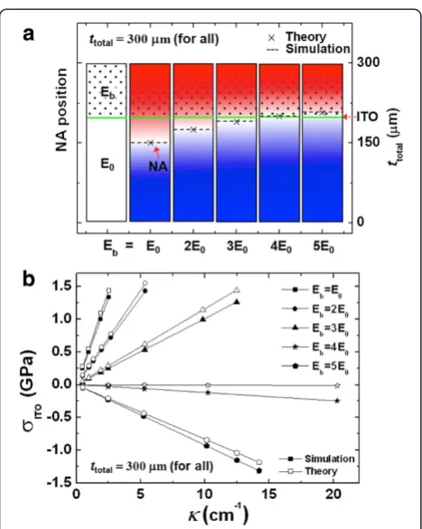
We investigated how the NA position varied with the elastic modulus and thickness of the buffer layer. First, we considered the elastic modulus of the buffer layer (Eb). We
assumed an 80-nm-thick ITO layer on a PES substrate with an elastic modulus ofE0and a thickness of 200μm. When
a 100-μm-thick buffer layer was placed on the ITO layer,
we calculated the NA position using the NA theory from Equations 1 and 3, and along with a simulation using an ABAQUS 6.10 simulator (Dassault Systèmes Simulia, Provi-dence, RI, USA) with various values forEb. The calculated
results from the two methods were about the same, as shown in Figure 3. The NA position gradually became closer to the ITO layer as Eb increased, and they closely
corresponded whenEbbecame four timesE0, as shown in
Figure 3a. Then, whenEbbecame larger than 4E0, the NA
position separated from the ITO layer again. In other words, when the thickness of the buffer layer was selected, a specificEbmade it possible to position the ITO layer at
the NA. Figure 3b shows the corresponding maximum stress of the ITO layer according to the bending curvature (κ) for variousEb. WhenEbis equal toE0, tensile stress in
the ITO layer occurred because the NA position was located below the ITO layer, and this tensile stress gradually decreased asEbincreased to 4E0. Then, whenEbwas larger
than 4E0, compressive stress in the ITO layer occurred
be-cause the NA position was located above the ITO layer, and this compressive stress increased proportionally asEb
increased over 4E0. In other words, the maximum stress
on the ITO decreased proportionally asEbincreased up to
4 E0because the NA position was gradually closer to the
[image:3.595.57.539.89.355.2]ITO layer, and this effect brought about the results that increased the critical bending curvature (i.e., the smallest radius that the layers can be bent before the critical bending radius decreased, which is the fracture). In particular, in the Figure 2Load-displacement data for depth-sensing indentation experiment.(a) ITO, (b) PES, (c) PI, (d) ZnO. (S: contact stiffness,P: load,
[image:3.595.56.291.662.735.2]h: distance).
Table 1 Mechanical properties of ITO, PES, PI, and ZnO
Material ITO PES PI ZnO
Thickness (nm) 80 200 × 103 50 × 103 520
Modulus (GPa) 116 4.6 2.0 96.1
Standard deviation 3.69 0.03 0.07 3.3
case of Eb= 4 E0, when the maximum bending curvature
was 20 cm−1 (i.e., maximum bending radius was 500μm), the maximum stress was only about 250 MPa. Considering the yield strength of 1.2 GPa for ITO [26], it would not lose its inherent properties up to a critical bending radius of 100μm. In Figure 3, the slight difference in the results be-tween the theory and simulation was probably caused by the assumption that a cross-sectional area of the beam in the theory does not change when being bent (i.e., the theory does not consider the effect of Poisson's ratio).
Next, we considered the effect of the thickness of the buf-fer layer (tb) on the NA, as shown in Figure 4. We assumed
that an 80-nm-thick ITO layer was on a PES substrate with E0and a thickness of 200μm. WhenEbwas the same asE0,
the NA position was calculated with various values for tb
using the two methods mentioned above. When tb was
lower thant0, the NA position was located below the ITO
layer, and the tensile stress in the ITO layer occurred. The NA position became closer to the ITO layer astbincreased
up to t0, and this corresponding tensile stress gradually
decreased. Then, whentbwas larger thant0, the ITO layer
was located above the NA position, and the compressive stress in the ITO layer occurred. This compressive stress increased proportionally astbincreased overt0, as shown in
Figure 4a. In the case of tb=t0, considering the yield
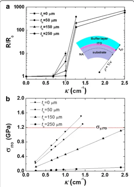
strength of ITO, the critical bending curvature was about 60 cm−1 (i.e., the bending radius was about 167 μm), as shown in Figure 4b. Thus, by controlling the elastic modu-lus and thickness of a buffer layer, the NA position could be easily controlled, and the mechanical bending stability of the ITO layer could be significantly increased when the ITO layer was located at the NA position. In order to confirm the theoretical behavior of the NA and the corre-sponding mechanical durability, we performed an experi-ment in which the electrical resistance of ITO films was measured as the bending curvature increased. PI was adopted as a buffer layer on an ITO film (see the inset in Figure 5a), and we increased thetbof PI from 0 to 250μm.
The PI thickness was simply controlled using a PI adhesive tape with a thickness of 50μm, and we confirmed that the elastic modulus of the PI film does not change by the nano-indentation test when the thickness increased from 50 to 250μm. Figure 5a shows the dependence of the two-probe resistance for PI(tb)/ITO/PES on bending curvature
κ, and R/R0indicates the bent-to-unbent ratio of the
[image:4.595.57.291.85.378.2]two-probe resistance. The initial curvature of all the structures was almost flat up to 0.7 cm−1. When the curvature was higher than 0.7 cm−1, the resistance for all of the structures Figure 3Behavior of NA position only by consideringEb.(a) NA
position depending onEbby the NA theory and simulation (red:
[image:4.595.304.539.88.383.2]tension, blue: compression). (b) Maximum stress of ITO layer according toκfor variousEb.
Figure 4Behavior of NA position only by considering thetbof
a buffer layer.(a) NA position depending ontbby the NA theory
increased. As the thickness of the buffer layer increased, the change in resistance decreased. In particular, in the case of a buffer layer with a thickness of 250μm, the re-sistance was almost zero up to a curvature of 1 cm−1. Then, the resistances for structures with buffer layer thick-nesses of 0, 50, and 150μm could not be obtained for cur-vatures of 1, 1.2, and 2.5 cm−1, respectively. This was caused by a fracture of the ITO layer in the structures. Thus, we confirmed that the bendability of the ITO film could be increased by employing a buffer layer, and this was because the maximum bending stress of the ITO layer was decreased by locating the ITO layer near the NA pos-ition based on Equation 3.
Again, to confirm these results, we performed a simula-tion of the PI(tb)/ITO/PES structure to determine how the
maximum bending stress of ITO changed with the buffer layer thickness. Based on the simulated results, we found when the fracture of the ITO layer occurred for each speci-men and compared the simulated results with the experi-mental results. As shown in Figure 5b, the yield of ITO layers consisting of a buffer layer with thicknesses of 0, 50, and 150 μm respectively occurred at curvatures of about
1.1, 1.3, and 2.6 cm−1, and these results were in close agree-ment with those of the experiagree-ment. However, the structures with a buffer layer showed relatively high-level resistances when the bending curvature was larger than 1 cm−1(i.e.,R/ R0were greater than 100). This might be caused by the
im-perfect bonding of the buffer layer because the PI adhesive tapes were not firmly bound to one another when the thickness was increased. Even though the structures with a buffer layer showed relatively high resistance, for the above-mentioned reason, the simulation and experiment demon-strated that ITO-based structures with a buffer layer are highly reliable and durable during bending. As stated earl-ier, to significantly increase the bendability of flexible devices, we should place the ITO layer at the NA position.
So far, although we independently considered the effects ofEbandtb, when the other was fixed, all of them
depend-ently had an influence on the NA position. Thus, it is ne-cessary to develop the governing design rule for the bendability optimization, considering the relationship be-tween them. To deduce this relationship, we considered a simple multilayer model composed of three kinds of mate-rials, including the substrate (E0,t0), ITO (EI,tI), and buffer
layer (Eb,tb), as shown in Figure 6 (inset). From Equations 1
and 3, the equation for locating the NA becomes
Eb
Z
bydA
þEI
Z
IydA
þE0
Z
0ydA
¼0 ð4Þ
Assuming that the NA is at the center of the ITO, this equation can be obtained by substituting the expressions foryandAinto the expressions fortandw; thus,
Eb tbþtI
2
tbwþEIð Þ0 tbwE0 t0þtI
2
t0w¼0 ð5Þ
[image:5.595.57.290.89.415.2]whereAandware the cross-sectional area and width, re-spectively. Because the ITO layer for optical electronics is Figure 5Experimental verification of enhanced bendability of
ITO-based thin films according to thetbof PI.(a) Two-probe
resistance and (b) maximum stress of ITO layer for PI/ITO/PES on bending curvatureκ(σy: yield strength).
Figure 6Relationship betweenEbandtb.Considering a simple
[image:5.595.305.538.517.692.2]very thin (tI <<t0,tb), we can settIto zero. Thus, the
re-lationship betweenEbandtbis as follows:
Ebt2b¼E0t20 ð6Þ
Equation 6 can be solved fortbin terms ofEb,
obtain-ing the followobtain-ing relationship:
tb¼t0
ffiffiffiffiffi
E0
p
1ffiffiffiffiffi
Eb
p ð7Þ
This equation shows that tb is inversely proportional
to the square root of Eb, as shown in Figure 6. This
equation provides the design rule that can optimize the bendability of flexible optical nanoelectronics by tuning both the elastic modulus and thickness of a buffer layer. In other words, when designing flexible optical electron-ics, we can choose a specific material of any thickness and improve not only the mechanical bendability, but also the electrical efficiency. Because there is an enor-mous variety of materials and structures in flexible elec-tronics, our design rule can have a great effect on these devices. Even though we assumed that one fragile layer exists between the substrate and buffer layer, this design rule can be applied to optical nanoelectronics with mul-tiple fragile layers such as conductive oxides, including ITO, ZnO, and AZO, because the thickness of the con-ductive oxides for optical electronics is typically less than a few hundred nanometers and all fragile layers are located near the NA. Although the multiple layers exist in OSCs, their effect in Equation 5 is very small and is negligible. Thus, we can obtain the optimized thickness of each buffer layer from Equation 7 when the buffer layers with various material properties are respectively employed.
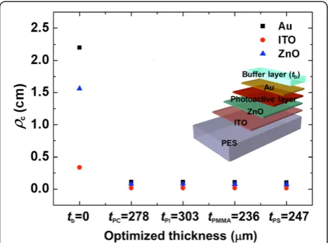
To demonstrate our design rule for the bendability optimization of flexible electronics with multiple fragile layers, we applied different buffer materials (polycarbonate (PC), PI, poly(methyl methacrylate) (PMMA), and poly-styrene (PS)) to inverted OSCs with an ITO optical win-dow. The inverted OSC was composed of five layers, including PES (200μm), ITO (80 nm), ZnO (50 nm), poly (3-hexylthiophene)/[6,6]-phenyl-C61-butyric acid methyl
ester blend photoactive layer (E= 6.02 GPa, ν= 0.35, t= 100 nm), and Au (E= 69.8 GPa, ν= 0.44, t= 70 nm) [27,28]. To optimize the bendability of flexible electronics, the thickness of each buffer material was calculated based on the elastic modulus of buffer layers from Equation 7. The optimized thicknesses of PC, PI, PMMA, and PS were 278, 303, 236, and 247 μm, respectively. Figure 7 shows the critical bending radius (ρc) for inverted OSCs with
dif-ferent buffer materials from the simulation, considering the yield strength for each material (σy= 200 MPa for ZnO
andσy= 120 MPa for Au) [29]. While theρcof the device
with no buffer layer was only about 2.2 cm due to a
fracture of Au, theρcof each device with the buffer
mater-ial, including optimized PC, PI, PMMA, and PS, were 1.11, 1.11, 1.09, and 1.05 mm, respectively. All of the inverted OSCs with different buffer materials to which our design rule was applied had almost the same ρc, which
was at least 20 times lower than that with no buffer layer. These results clearly showed that our design rule could optimize the bendability of flexible nanoelectronics with various buffer materials. Further, the ρc of each
compo-nent in the device without a buffer layer such as Au, ITO, and ZnO varied from 2.2 to 0.34 cm, depending on their material properties, whereas in the case of the device with a buffer layer,ρcvalues of the components were on a
simi-lar level (i.e., low ρc), regardless of their properties. This
was because all of the thin fragile components were located near the NA position, and this result clearly showed that our design rule can also be applied to flexible optical nanodevices with multiple thin, fragile layers. In other words, no matter what buffer materials and thin components are used in the devices, the bendability can be significantly enhanced by the design rule based on NA engineering. Thus, this design rule could provide valuable guidance for the design and performance optimization of flexible optical nanoelectronics.
Conclusions
[image:6.595.305.539.89.262.2]bendability optimization of various flexible nanoelectro-nics. Furthermore, our design rule was applied to inverted OSCs with various buffer materials, and we confirmed that all of the OSCs showed excellent bend-ability, whatever buffer materials were chosen. Thus, our strategy may provide a wide range of opportunities for a variety of flexible electronic applications.
Competing interests
The authors declare that they have no competing interests.
Acknowledgments
This work was supported by the National Research Foundation of Korea (NRF) grant funded by the Ministry of Education, Science and Technology (MEST) (Nos. 2010–0029120 and 2010–0018457), the Basic Science Research Program through the NRF funded by the MEST (2011–0008589), and a grant (Code No. 2011–0032154) from the Center for Advanced Soft Electronics under the Global Frontier Research Program of MEST. DC also acknowledges the financial supports by the Energy International Collaboration Research & Development Program of the Korea Institute of Energy Technology Evaluation and Planning (KETEP) funded by the Ministry of Knowledge Economy (MKE) (2011–8520010050) and by the Business for Cooperative R&D between Industry, Academy, and Research Institute funded Korea Small and Medium Business Administration in 2011 (Grant No. 48401).
Author details
1Department of Mechanical Engineering, Pohang University of Science and
Technology, San 31, Hyoja, Namgu, Pohang, Gyungbuk 790-784, Republic of Korea.2School of Integrated Technology, Yonsei University, 162-1, Songdo-dong Yeonsu-gu, Incheon 406-840, Republic of Korea.3Department of Mechanical Engineering, College of Engineering, Kyung Hee University, 1 Seocheon-dong, Giheung-gu, Yongin-si 446-701, Republic of Korea.
Authors’contributions
SL and J-YK equally contributed to this work. WH and DC conceived the initial idea and designed the schemes. SL, J-YK, and DY performed the numerical simulations, and HC and JY performed the experiments. WH, DC, J-YK, and YTK, with partial contributions from SL, characterized the results. DC and SL wrote the paper with partial contributions of WH and J-YK. All authors discussed the results, commented on the manuscript, and approved the final manuscript.
Received: 12 February 2012 Accepted: 15 May 2012 Published: 15 May 2012
References
1. Normura K, Ohta H, Takagi A, Kamiya T, Hirano M, Hosono H: Room-temperature fabrication of transparent flexible thin-film transistors using amorphous oxide semiconductors.Nature2004,432:488–492.
2. Han L, Song K, Mandlik P, Wagner S:Ultraflexible amorphous silicon transistors made with a resilient insulator.Appl Phys Lett2010,96:042111. 3. Sekitani T, Lba S, Kato Y, Noguchi Y, Someya T:Ultraflexible organic
field-effect transistors embedded at a neutral strain position.Appl Phys Lett2005,87:173502.
4. Jedaa A, Halik M:Toward strain resistant flexible organic thin film transistors.Appl Phys Lett2009,95:103309.
5. Zschieschang U, Ante F, Yamamoto T, Takimiya K, Kuwabara H, Ikeda M, Sekitani T, Someya T, Kern K, Klauk H:Flexible low voltage organic transistors and circuits based on a high mobility organic semiconductor with good air stability.Adv Mater2010,22:982–985.
6. Chiang CJ, Winscom C, Bull S, Monkman A:Electroluminescence characterization of FOLED devices under two type of external stresses caused by bending.Org Electron2009,10:1268–1274.
7. Ju S, Facchetti A, Xuan Y, Liu J, Ishikawa F, Ye P, Zhou C, Marks TJ, Janes DB:
Fabrication of fully transparent nanowire transistors for transparent and flexible electronics.Nature Nanotech2007,2:378–384.
8. Wang GF, Tao XM, Wang RX:Flexible organic light-emitting diodes with a polymeric nanocomposite anode.Nanotechnology2008,19:145201.
9. Sekitani T, Zschieschang U, Klauk H, Someya T:Flexible organic transistors and circuits with extreme bending stability.Nature Mater2010,
9:1015–1022.
10. Ghosh D, Ghosh P, Tanemura M, Haysahi A, Hayashi Y, Shinji K, Miura N, Yusop MZ, Asaka T:Highly transparent and flexible field emission devices based on single-walled carbon nanotube films.Chem Commun2011,
47:4980–4982.
11. Minami T, Yamamoto T, Toda Y, Miyata T:Transparent conducting zinc-co-doped ITO films prepared by magnetron sputtering.Thin Solid Films2000,373:189–194.
12. Yaglioglu B, Yeom HY, Paine DC:Crystallization of amorphous InO–10 wt % ZnO thin films annealed in air.Appl Phy Lett2005,86:261908. 13. Minami T:Present status of transparent conducting oxide thin-film
development for indium-tin-oxide (ITO) substitutes.Thin Solid Films2008,
502:104–106.
14. Wu J, Becerril HA, Bao Z, Liu Z, Chen Y, Peumans P:Organic solar cells with solution-processed graphene transparent electrodes.Appl Phy Lett2008,
92:263302.
15. Park SK, Han JI, Moon DG, Kim WK:Electrical characteristics of poly (3-hexylthiophene) thin film transistors printed and spin-coated on plastic substrates.Jpn J Appl Phys2003,42:623–629.
16. Oliver WC, Pharr GM:Improved technique for determining hardness and elastic modulus using load and displacement sensing indentation experiments.J Mater Res1992,7:1564–1567.
17. Seitzman LE:Mechanical properties from instrumented indentation: uncertainties due to tip-shape correction.J Mater Res1998,13:2936–2944. 18. Herrmann K, Jennett NM, Wegener W, Meneve J, Hasche K, Seemann R:
Progress in determination of the area function of indenters used for nanoindentation.Thin Solid Films2000,377:394–400.
19. Thurn J, Cook F:Simplified area function for sharp indenter tips in depth-sensing indentation.J Mater Res2002,17:1143–1149.
20. Lu C, Danzer R, Fischer FD:Scaling of fracture strength in ZnO: effects of pore/grain-size interaction and porosity.J Eur Ceram Soc2004,
24:3643–3651.
21. James EM:Polymer Data Handbook. New York: Oxford University Press; 1999. 22. Kaiyang Z, Furong Z, Jianqiao H, Lu S, Keran Z, Hao G:Investigation on the
origin of green luminescence from laser-ablated ZnO thin film.Thin Solid Films2003,443:60–66.
23. Seitz JT:The estimation of mechanical properties of polymers from molecular structure.J Appl Polym Sci1993,49:1331–1351.
24. Yang PF, Wen HC, Jian SR, Lai YS, Wu S, Chen RS:Characteristics of ZnO thin films prepared by radio frequency magnetron sputtering.Microelec Relia2008,48:389.
25. Qi D, Hinkley J, He G:Molecular dynamics simulation of thermal and mechanical properties of polyimide–carbon-nanotube composites. Modelling Simul Mater Sci Eng2005,13:493–507.
26. Bouten PCP, Sikkeveer PJ, Leterrier Y:Mechanics of ITO on plastic substrates for flexible displays. InFlexible Flat Panel Displays. Edited by Crawford GP. Chichester: John Wiley & Sons; 2005:99–120.
27. Tahk D, Lee HH, Khang DY:Elastic moduli of organic electronic materials by the buckling method.Marcromolecules2009,42:7079–7083. 28. Diethiker M, Nyilas RD, Solenthaler C, Spolenak R:Nanoindentation of
single-crystalline gold thin films: correlating hardness and the onset of plasticity.Acta Materialia2008,56:3887–3899.
29. Chen CQ, Zhu J:Bending strength and flexibility of ZnO nanowires.Appl Phys Lett2009,90:043105.
doi:10.1186/1556-276X-7-256
Cite this article as:Leeet al.:Bendability optimization of flexible optical nanoelectronics via neutral axis engineering.Nanoscale Research Letters