Theoretical Characterisation of
Spheroidal PbSe/PbS Core/Shell
Colloidal Quantum Dot
Heterostructures
Thomas M. Walsh
Ph.D. Thesis
University of Salford
School of Computing, Science, and Engineering
C O N T E N T S
1 i n t r o d u c t i o n 1
1.1 Photovoltaics as a Power Source . . . 3
1.2 Thesis Premise . . . 3
1.3 Thesis Outline . . . 5
2 p h o t ov o lta i c s o l a r c e l l d e v i c e s 7 2.1 An Abridged History of Photovoltaic Solar Cell Technology . . . . 8
2.2 The Semiconductor p-n Junction . . . 10
2.3 The Photovoltaic Effect . . . 12
2.4 Carrier Relaxation Dynamics . . . 14
2.4.1 Fermi’s Golden Rule . . . 15
2.4.2 Carrier-Carrier Scattering . . . 18
2.4.3 Carrier-Phonon Scattering . . . 21
2.5 Radiative Carrier Recombination . . . 24
2.6 Nonradiative Recombination Mechanisms . . . 26
2.6.1 Auger Recombination . . . 26
2.6.2 Shockley-Read-Hall Recombination . . . 30
2.7 The Shockley-Queisser Limit of Efficiency . . . 33
2.8 Chapter Summary . . . 34
3 t h i r d g e n e r at i o n p h o t ov o lta i c s 35 3.1 Multijunction Solar Cells . . . 35
3.2 Intermediate Band Solar Cell devices . . . 39
3.3 Impact Ionisation . . . 41
3.4 Chapter Summary . . . 44
Contents ii
4 q ua n t u m na n o c r y s ta l s 46
4.1 Quantum Confinement . . . 47
4.1.1 Unconfined Systems—The Bulk . . . 48
4.1.2 Confinement in One Dimension—Quantum Wells . . . 49
4.1.3 Confinement in Two Dimensions—Quantum Wires . . . 50
4.1.4 Confinement in Three Dimensions—Quantum Dots . . . 51
4.2 Nanocrystal Quantum Dots—Artificial Atoms . . . 52
4.3 Efficient Carrier Multiplication in Nanocrystal Quantum Dots . . . 54
4.3.1 Phonon Bottleneck . . . 55
4.4 MEG enhancement in Core/Shell Quantum Dot Heterostructures . 57 4.4.1 Observation of MEG in real systems . . . 60
5 l e a d-c h a l c o g e n i d e q ua n t u m d o t s 63 5.1 The Unusual Electronic Properties of PbX Compounds . . . 65
5.2 Carrier Effective Masses . . . 67
5.3 Spheroidal quantum dots . . . 69
6 t h e o r y 71 6.1 Limits of ab Initio methods . . . 71
6.2 kkk·pppPerturbation Theory . . . 72
6.2.1 The Parabolic Effective Mass Approximation . . . 73
6.2.2 The Single-Particlekkk·pppPerturbation Method . . . 74
6.2.3 The Spin-Orbit Interaction . . . 77
6.2.4 The Four-Bandkkk·ppp Equation for Lead-Salt Quantum Dots . 78 6.2.5 Selection Rules . . . 81
6.3 Expansion in the Plane Wave Basis . . . 82
6.4 The Configuration Interaction Method . . . 85
Contents iii
6.5.1 The Hellmann-Fenyman Theorem . . . 100
6.5.2 Radiative Carrier Recombination . . . 101
6.6 Multiple Exciton Generation . . . 104
7 r e s u lt s 109
7.1 Single-Particle States . . . 110
7.1.1 Spherical PbSe QDs . . . 111
7.1.2 PbSe/PbS Core/Shell Quantum Dot Heterostructures . . . 115
7.1.3 Spheroidal PbSe and PbSe/PbS PbS Nanocrystal Quantum
Dot Structures . . . 124
7.2 Excitonic Properties . . . 132
7.2.1 Excitonic states of PbSe core-only NQDs . . . 136
7.2.2 Excitonic states of PbSe/PbS Quantum Dot Heterostructures138
7.2.3 Excitonic States of Spheroidal PbSe/PbS Quantum Dot
Het-erostructures . . . 143
7.3 Radiative Carrier Lifetimes . . . 145
7.4 Multiple Exciton Generation . . . 149
7.4.1 Order of Magnitude Analysis of CM Matrix Elements . . . . 151
8 c o n c l u s i o n s 154
8.1 Future Directions . . . 155
Appendices 158
a c o m m u tat i o n r e l at i o n s f o r f e r m i o n s 159
b c i m at r i x e l e m e n t s f o r d i r e c t c a r r i e r m u lt i p l i c at i o n (m e g)161
b.1 Single-Particle contributions . . . 162
b.2 Two-Particle contributions . . . 165
L I S T O F F I G U R E S
Figure1.1 Annual (black) and five-year (red) mean global
tempera-ture anomaly relative to the period 1951-1980. Inset:
At-mospheric CO2 levels over the period1958-2015. Data
ob-tained from NASA’s public access records, which may be
found in reference [3]. . . 2
Figure2.1 Metallic (left), semiconductor (centre), and insulator (right)
band structures about the Fermi level (dashed line). . . 7
Figure2.2 Schematic of a semiconductor p-n junction. Electrons (holes)
diffuse into the p-region (n-region) and form a depletion
region at the interface containing no free carriers and
es-tablishing device bias. Photogenerated charge carriers
in-side the junction are quickly separated by the intrinsic
fieldEEE. . . 11
Figure2.3 Photoabsorption in a photovoltaic cell. High energy
pho-tons (blue) excite electrons (holes) far above (below) the
CBM (VBM) by energy ∆Ee (∆Eh). The cell is transparent
to photons of sub-bandgap energy. . . 13
Figure2.4 Schematic of thermalisation processes of hot carriers: a)
like-carrier scattering produces independent Boltzmann
distributions in the bands; b) electron-hole scattering
equi-librates the distributions; c) carriers cool via phonon
emis-sion (small Auger component); d) carriers are extracted or
recombine either radiatively or nonradiatively. . . 16
List of Figures v
Figure2.5 For every scattering process (kkk1,kkk2)→ (kkk0
1,kkk 0
2) between
in-distinguishable fermions, there exists an equivalent
pro-cess (kkk1,kkk2)→(kkk02,kkk 0
1). . . 19
Figure2.6 Schematic of various Auger processes: a) an electron
re-combines with a hole–the excess energy is transferred to a
secondary electron in the CB; b) an Auger process similar
to in a) is stimulated by phonon; c) an electron drops into
a trap state; d) the electron continues from the trap state
to the VB. . . 27
Figure2.7 Four SRH processes: a) electron capture, b) electron
emis-sion, c) hole capture, d) hole emission. Here, the trap level
lies in the middle of the band gap. The trap energy level
is not in general coincident with the Fermi level (dashed
line). . . 31
Figure3.1 Schematic of a multijunction solar cell. A typical
multi-junction may consist of (top to bottom) GaInP/GaInAs/Ge
separated by tunnel diodes. The bandgap energies of the
subcells are1.8eV/1.4eV/0.7eV. . . 36
Figure3.2 A solar cell containing an intermediate band within the
band gap of the intrinsic region of a p-i-n heterojunction.
The intermediate band should ideally be half-populated
in order to both accept electrons from the valence band
and supply electrons to the conduction band. The
inter-mediate band should also be aligned with the Fermi energy. 40
Figure3.3 Impact ionisation (left) is the inverse of the direct Auger
List of Figures vi
Figure4.1 Schematic of a multiple quantum well structure. Charge
carriers are confined to the wells by the potential at the
interfaces. The region between the dotted lines forms a
type I heterojunction. . . 50
Figure4.2 Cross-section of a quantum nanowire Carrier are confined
along the lateral dimensions of the nanowire. . . 51
Figure4.3 Density of states for a) bulk (3D), b) quantum well (2D),
c) quantum wire (1D), and d) quantum dot (0D). . . 53
Figure4.4 Type-II band alignment for core/shell QD cross-section.
The core region is enveloped by a semiconductor with
band alignment such that a "staggered gap" interface is
formed. This results in an effective band gap being
estab-lished in the dot and carrier confinement to the core and
shell region (here, CB electrons are confined to the core,
while VB holes are confined to the shell. . . 58
Figure4.5 Positive and negative trions cause charge imbalance in
the dot. Each may recombine nonradiatively leading to
misidentification as biexcitons in early MEG investigations 62
Figure5.1 Top: rock-salt crystal structure of lead (black) selenide
(yellow). Bottom: Brillouin zone for the FCC lattice. The
HOMO and LUMO of the lead-salts are found at the
high-symmetryL-point of the Brillouin zone. . . 64
Figure5.2 Band structure near the extrema for: a) many zone-centre
direct bandgap materials, where the VB is split into light
hole (LH), heavy hole(HH), and spin split-off (SS) bands,
while the CB is spin-degenerate; and b) PbX with a
di-rect gap at the L-point, where both the CB and VB consist
of a single, four-fold degenerate band (exclusive of spin
List of Figures vii
Figure5.3 Bandstructure for PbSe. The bandgap is narrow and lies
at the L-point of the first Brillouin zone. This
bandstruc-ture was calculated via time-independent DFT (CASTEP)
using a PBE exchange-correlation functional. . . 67
Figure5.4 Spheroids of revolution are generated by rotating an
el-lipse about the c axis. For c < a, the spheroid is oblate
(left), while forc >a the ellipsoid is prolate (right). . . 69
Figure7.1 Single-particle states for spherical PbSe QDs of increasing
radius. The electron (hole) single-particle energy states
decrease (increase) as the radius of the dot is increased. . . 112
Figure7.2 Energy level diagrams for three representative QDs. The
energy levels of the smaller dot (RRR = 18.36 Å, left) are
sparse, and the bandgap is large. As the size of the QD
in-creases, the energy levels become bunched, and the bandgap
closes. The spectrum becomes more "band-like" as the size
of the dot increases. Each of the levels shown are two-fold
degenerate. . . 113
Figure7.3 Single-particle en−h0 transition energies for QDs of
in-creasing radius. The size-dependence and energy
sepa-ration follow a similar trend as seen for the CB states in
figure 7.1. . . 114
Figure7.4 Momentum matrix elements for spherical PbSe core-only
QDs of radius a) 18.36 Å, b) 24.48 Å, and c) 30.60 Å. The
x/y polarised transitions are of uniform magnitude and
greater than those polarised in the zdirection. Forbidden
transitions are shown in black beneath thex-axis. . . 116
Figure7.5 Single-particle bandedge energy states (e0,h0) for a
List of Figures viii
Figure7.6 Single-particle energy states for a spherical PbSe QD of
radius 30.60 Å with progressively larger PbS shells. . . 119
Figure7.7 Energy level diagrams for QDS of PbSe core radius 30.60 Å
and PbS shell thicknesses of 0 angstrom (no shell), 5.94 Å
(aPbS), and 11.87 Å (2aPbS). Increased shell thickness
re-duces the effective bandgap energy and causes bunching
of the sp states. . . 120
Figure7.8 Single-particleen−h0interband transition energies
spher-ical PbSe QD of radius 30.60 Å for progressively thicker
PbS shells. . . 121
Figure7.9 First few transitions for spherical PbSe QD of radius 30.60 Å
with a) no shell, b) PbS shell of thickness 5.94 Å, and c)
PbS shell of thickness 11.87 Å. Increased shell thickness
results in weakening of the interband momentum matrix
elements (plotted here on axes of equal increment), while
the observed red-shift is a consequence of the quantum
size effect. . . 122
Figure7.10 Electron (left) and hole (right) wavefunctions for the three
lowest energy states (n = 1, 2, 3) in a spherical QD of core
radius 30.60 Å and shell thickness 23.744 Å. In this energy
range, the electron is confined to the core region, while
the hole wavefunction permeates the whole QD structure.
The reduced overlap of the carrier wavefunctions
dimin-ishes the strength of the interband momentum matrix
el-ements. . . 123
Figure7.11 The anisotropy of the betweenx/yandz-polarisede0−h0
transition for representative spherical QDs of various core
List of Figures ix
Figure7.12 Single-particle states for spheroidal PbSe QDs of varying
ellipticity. The c-axis is elongated by: a) 5%; b) 10%; and
c)15% of the a-axis . . . 127
Figure7.13 Energy states of spheroidal QDs with semi-minor axis a=
30.60 Å. For the dots presented, each successive
elonga-tion of 5% reduces the effective bandgap on the order of
10 meV. . . 128
Figure7.14 en−h0 transition for core QDs of increasing size. The
c-axis is elongated by: a) 5%; b) 10%; and c) 15% of the
a-axis . . . 129
Figure7.15 First few optically bright interband momentum matrix
el-ements for PbSe QDs with a = 30.60 Å and a) c = a, b)
c = a+ 5%, and c) c =a+ 10%. Symmetry breaking results
in anisotropy between the x and y-polarised momentum
matrix elements in addition to the pre-existing x/z and
y/zanisotropy. . . 130
Figure7.16 Anisotropy between x-polarised and y-polarised
momen-tum matrix elements for QDs elongated along thex(h¯1¯12i)
direction. QDs with no shell (left), shell of one lattice
con-stant (centre), and shell of two lattice concon-stants (right) are
shown. The anisotropy is on the order of 1%, being
in-creased for larger ellipticity, and for QDs of smaller volume.131
Figure7.17 Band-edge energy states for QDs as a function of shell
thickness. The c-axis is elongated by: a) 5%; b) 10%; and
c)15% of the a-axis . . . 133
Figure7.18 en −h0 transitions for spheroidal QDs with a =30.60 Å.
The c-axis is elongated by: a) 5%; b) 10%; and c) 15% of
List of Figures x
Figure7.19 Linear variation of the HOMO and LUMO states as a
func-tion of the ratio of the axes of the spheroid. The variafunc-tion
is larger for smaller QDs. . . 135
Figure7.20 Excitonic energies have been generated via mixing of 12
electron and 12 hole sp states. The energies presented
have been averaged over the energy complex in which
they are found. . . 137
Figure7.21 Momentum matrix elements associated with excitonic states
for PbSe QDs of radius a) 18.36 Å, b) 24.48 Å, and c) 30.60 Å.
Matrix elements are split across energy complexes, while
magnitude of the elements is twice as large as in the
single-particle case. . . 139
Figure7.22 Lowest energy exciton state for QDs of varying core radii
as a function of shell thickness. . . 140
Figure7.23 Excitonic energy spectra for core/shell PbSe QD
heterostruc-tures with core radius 30.60 Å with increasing shell
thick-ness. . . 140
Figure7.24 The full spectrum of excitonic states generated by mixing
of 12electron and 12hole single-particle states as a
func-tion of shell thickness for QDs of core radii: a) 18.36 Å; b)
24.48 Å; c) 30.60 Å; and d) 36.72 Å. . . 141
Figure7.25 First few momentum matrix elements for QDs of core
ra-dius 30.60 and a) no shell, b) 5.94 Å, and c) 11.87 Å.
Ad-dition of the PbS shell reduces the energy associated with
the momentum matrix elements. The magnitude of the
elements is moderately reduced for thicker shells. . . 142
Figure7.26 Binding energyBXfor the lowest energy exciton for
spher-ical QDs of varying core radius and shell thickness. The
List of Figures xi
Figure7.27 Excitonic energy spectrum for QDs with a = 30.60 Å for
increasing shell thickness. QDs are elongated by a) 5%,
b) 10%, and c) 15%. Elongation of a single axis leads to
reduction in the energy spectrum on the order of tens of
millielectronvolts. . . 144
Figure7.28 Momentum matrix elements of core-only, a= 30.60 Å QDs
with elongation a) 5%, b) 10%, and c) 15%. Increasing
ellipticity of the dot increases the transverse-transverse
anisotropy for all exciton states. . . 146
Figure7.29 Lifetimes for radiative recombination between bandedge
states for several core sizes as a function of shell thickness.
The QDs are elongated by a)0%, b) 5%, c) 10%, and d),15%.147
Figure7.30 Radiative carrier lifetimes for the lowest exciton state.
Ex-citonic binding reduces the core-only lifetimes on the
or-der of 1 ns. Strong size-dependence of excitonic states
in-creases the carrier lifetime for thick shells. . . 150
Figure7.31 The width of the Lorentzian distribution introduced in
equation 6.124 plays a large role in the determination of
the scattering rate. Improper choice ofΓresults in
L I S T O F TA B L E S
Table2.1 Energy threshold and coefficients for Auger
recombina-tion for sample bulk semiconductors. . . 29
Table3.1 Maximum efficiency of an N-junction solar cell. Values
taken from1
reference [71] and2reference [72]. . . 38
Table4.1 Exciton Bohr radii for various materials. Values taken
from1
reference [21] and2reference [94]. . . 48
Table4.2 The dimensionallity of confinement for different structures. 48
Table6.1 Input parameters for the kkk·ppp Hamiltonian [157] . . . 79
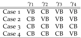
Table B.1 Contributing permutations of {γ}. Cases 1 and 2
corre-spond to the process involving an initially hot hole, while
cases 3 and 4 represent the direct carrier multiplication
process where the hot carrier is an electron. . . 165
[image:13.595.151.527.178.482.2]A C K N O W L E D G E M E N T S
I would like to extend my unreserved thanks to the many people who have made
this work possible. Without their support and encouragement, the current work
could not exist.
First and foremost, to my supervisor Professor Stanko Tomi´c. His expertise
and guidance have made this work possible. His patience and diligence as a
mentor have been invaluable, and helped to develop my skills as a researcher.
To Dr. Jacek Milosewski, for many invaluable discussions on colloidal
quan-tum dots, theoretical modelling techniques, general programming advice,
col-laborative efforts, and constant encouragement. Also for occasional lifts in his
car.
To Mark Lundie, for invaluable discussions on quantum mechanics and
theo-retical condensed matter physics, as well as for his diligent work in maintaining
the local cluster on which all calculations presented in this work were performed.
To all of the staff and students in the Physics department at the University of
Salford for their continued support over the last three years, especially Professor
Ian Morrison, Dr. Graham McDonald and Bruce Lewis for keeping the
depart-ment in good working order. To all of the other residents of the postgraduate
office, especially Slobodan ˘Ci˘ci´c, Alex Marshall, Dean Smith and Simon Steel,
for many interesting, if not strictly relevant, discussions.
To the many members of staff in the postgraduate research and finance offices
at the University of Salford, in particular Catriona Nardone and Vanda
Thomlin-son, for their help and extreme patience with matters of paperwork, especially
when things did not go according to plan.
Acknowledgements xiv
To the organisers and committees of the various conferences and meetings at
which I have been permitted to present my work, as well as the various scientists
and scholars with whom I have had the opportunity to spoke with at these
events, of which there are too many to name.
Finally, I would like to thank the EPSRC for doctoral training account (DTA)
funding over the last three-and-a-half years, as well as the Royal Society for
the equipment provided by their grant (No. RG120558): "High Performance
xv
Abstract
Nanocrystal quantum dots (NQDs) show great promise in the advancement of
the field of photovoltaics. While the maximum efficiency of conventional solar
cell (SC) devices is limited to∼31% (Shockley-Queisser limit), devices based on
NQDs may attain a maximal thermodynamic efficiency of 42% through the
ex-ploitation of multiple exciton generation (MEG). In this process, several
electron-hole pairs are created by the absorption of a single high energy photon, as
op-posed to the single excitons created in conventional solar cell devices. IV-VI
semiconductor nanocrystals (PbS, PbSe) are of particular interest as candidates
for the exploitation of MEG due to the narrow band gap, high confinement
en-ergies, and long radiative carrier lifetimes observed in these systems. In order
to realise the full potential of MEG devices, full characterisation of the
optoelec-tronic properties of the underlying nanoparticles is desirable.
While the size-dependent properties of NQDs are well understood, the effects
of NQD shape are less so. This thesis investigates the effect of ellipticity on the
optoelectronic properties associated with spheroidal NQDs. To this end, a
four-band, anisotropic, and radially variant kkk·ppp system Hamiltonian is expanded in a
planewave basis in order to calculate single-particle eigenenergies and
eigenfunc-tions of colloidal PbSe/PbS core/shell heterogeneous NQDs of varying
elliptic-ity. Many-body effects are accounted for via a full configuration interaction (CI)
Hamiltonian, the basis of which is comprised of the single-particle states.
Exci-tonic and bi-exciExci-tonic corrections are then found by mixing of the basis states.
In this manner, such diverse electronic and optical properties as quasi-particle
binding energies, momentum matrix elements, and charge carrier lifetimes, both
xvii
All results presented in this work have been obtained using the highly parallel
kppwcode, which has been augmented with new functionality pertaining to the
1
I N T R O D U C T I O N
The dominant means of energy production in the modern age are derived from
the burning of fossil fuels. Current projections indicate that by the year2040the
global demand for energy will increase by37% (a growth rate of between 1% to
2% year-on-year), while carbon emissions correspondingly increase by 16% [1].
It is thought, given current trends, that 84% of energy production will still be
derived from fossil fuel sources in2030, while economically recoverable oil, coal,
and gas reserves are expected to be depleted by the years 2040, 2042, and 2112
respectively [2]. Moreover, the environmental damage caused by the burning of
fossil fuels is devastating. Recent climate data shows that global temperatures
have increased by almost 1◦C above the 20th century average (see figure 1.1)
[3]. It is generally agreed upon that should global temperatures 2◦C above
pre-industrial revolution levels, the effects of climate change will be catastrophic
and irreversible. To this end, the agreement reached by the COP 21 meeting
in Paris pledged to limit global warming to a maximum of 1◦C, with an ideal
limit of 0.5◦C [4]. If these targets are to be met, a paradigm shift toward more
environmentally friendly methods of power production must begin.
i n t r o d u c t i o n 2
1880 1890
1900 1910
1920 1930
1940 1950
1960 1970
1980 1990
2000 2010 -0.4
-0.2 0 0.2 0.4 0.6 0.8
Temperature anomaly [°C]
Annual mean 5-year mean 1965 1980 1995 2010
300 325 350 375 400
Atmospheric CO
2
[p.p.m.]
Figure1.1.: Annual (black) and five-year (red) mean global temperature anomaly
relative to the period 1951-1980. Inset: Atmospheric CO2 levels over
the period 1958-2015. Data obtained from NASA’s public access
1.1 p h o t ov o lta i c s a s a p o w e r s o u r c e 3
1.1 p h o t ov o lta i c s a s a p o w e r s o u r c e
Photovoltaic solar cell devices are cheap to manufacture, require very little
main-tenance, and are easily installed, even in remote locations. The current (second)
generation is limited in its attainable efficiency, however, by the intrinsic physical
processes by which the solar cell devices operate. The maximum theoretical
ef-ficiency, known as the Shockley-Queisser limit, has been obtained from detailed
balance calculations performed for an ideal solar cell. For a silicon based device
with the standard p-n junction arrangement under unconcentrated solar
illumi-nation, and assuming both the Sun and the solar cell to be perfect blackbodies,
the Shockley-Queisser limit is 30% [5]. The fundamental principles behind the
operation of the second generation photovoltaic solar cell device will be outlined
below.
Several schemes have been suggested by which the Shockley-Queisser limit
may be surpassed. These schemes, collectively referred to as third generation
solar cell devices, briefly comprise solar concentrators, multijunction solar cell
devices, intermediate band devices, and devices which promote and exploit the
process of multiple exciton generation (impact ionisation) [6–12]. Each of these
will be discussed in turn below.
1.2 t h e s i s p r e m i s e
The third generation of photovoltaic solar cell devices is widely expected to be
based upon semiconductor nanocrystal technology [13]. Such semiconductor
nanocrystals exhibit the effects of quantum confinement. When the size of the
nanocrystal is lesser than the de Broglie wavelength of its associated charge
carriers, the carrier wavefunctions are localised strongly within the volume of
the nanostructure, dramatically altering the electronic properties of the
1.2 t h e s i s p r e m i s e 4
or three spatial dimensions; the corresponding structures are termed quantum
wells (or quantum films), quantum wires, and quantum dots (QDs), respectively.
Confinement of the charge carriers has several effects on the electronic structure
of the nanocrystal, the most dramatic of which is the discretization of the energy
bands, along with an opening up of the interband energy gap (band gap) and
intraband energy gaps. The discrete nature of the electronic states in nanocrystal
quantum dots is high reminiscent of atomic energy spectra. Consequently,
quan-tum dots are occasionally given the moniker of "artificial atoms." It has been
predicted that, due to the phonon bottleneck effect observed in confined systems,
the process of impact ionisation (where several electron-hole pairs are produced
by absorption of a single photon) may be highly efficient in quantum dot based
solar cells [14].
To date, the vast majority of research has been directed towards spherical
quantum dots. From an experimental standpoint, this is largely due to the
ease with which spherical colloidal QDs may be synthesised, while,
computa-tionally speaking, spherical symmetry greatly simplifies the calculations
under-taken. In the current work, the effects of ellipticity (i.e. the eccentricity of the
ellipsoidal cross-section of an ellipsoid of rotation) are analysed for spheroidal
quantum dots from a theoretical standpoint. Due the their narrow bulk bulk
bandgaps, the QDs studied are of those consisting of lead-chalcogenide
nanos-tructures. Core/shell heterostructures of varying degrees of ellipticity are
mod-elled. Single-particle properties are found by solving the Four-band kkk·ppp
Hamil-tonian in the inverse space, with excitonic corrections being included via a
complementary configuration interaction (CI) calculation. This approach
al-lows for the calculation of such diverse properties as: single-particle and
many-particle eigenstates and eigenfunctions; exciton and biexciton binding energies;
dipole, momentum, and optical matrix elements; transition strength and
oscilla-tor strengths; absorption cross-sections; and radiative and nonradiative carrier
1.3 t h e s i s o u t l i n e 5
within the kppw code (originally developed by Stanko Tomi´c and colleges at
Daresbury Laboratory) [15].
1.3 t h e s i s o u t l i n e
The structure of the current work is as follows. Chapter2aims to familiarise the
reader with the current generation of solar cell technology. A brief outline of
the major developments in the field is given, followed by revision of the
funda-mental processes of solar energy conversion. The mechanisms by which energy
is lost in the conversion process are detailed, including relaxation dynamics and
recombination processes. The principles by which the maximum theoretical
effi-ciency of a conventional solar cell device may be calculated are summarised.
The following chapters detail the proposed methods by which the
Shockley-Queisser limit may be circumvented. Chapter3presents the various architectural
schemes by which solar cell efficiency may be enhanced, including multijunction
solar cell devices, intermediate band solar cells, and, perhaps most importantly,
direct carrier multiplication via the impact ionisation process. Chapter 4
ex-plores the effects of quantum confinement, and describes the mechanisms by
which confined systems may exhibit improved carrier multiplication
efficien-cies (known as multiple exciton generation in colloidal quantum dots).
Chap-ter5introduces in detail the unusual properties of bulk lead-chalcogenides, the
properties of lead chalcogenide based quantum dots, and discusses core/shell
PbSe/PbS heterostructures and spheroidal QD geometries.
The various modelling techniques used throughout the current work are
de-tailed in Chapter 6. The limits of ab initio methods are presented, and the kkk·ppp
perturbation theory introduced and extended to the four-band model used to
cal-culate single-particle properties of the lead-based quantum dots. An overview
of the plane wave basis in which the kkk·ppp Hamiltonian is represented is also
1.3 t h e s i s o u t l i n e 6
corrections to the eigenvalues of the kkk·ppp Hamiltonian is introduced. Finally,
calculation of carrier lifetimes for radiative recombination and for direct carrier
multiplication is discussed, with the explicit derivation of the required matrix
elements given in appendix B.
Chapter 7 presents the findings of the current work. Single-particle energy
states and the momentum matrix elements associated with interband transitions
are presented for PbSe QDs and PbSe/PbS QD heterostructures for both
spher-ical and spheroidal nanocrystals. It will be seen that in all cases anisotropy
exists between those transitions polarised along the h¯1¯12i/h1¯10i and the h111i
crystallographic directions, and that for QDs elongated along either transverse
direction, additional anisotropy is introduced between theh¯1¯12iandh1¯10i
direc-tions. Excitonic corrections are then added to the single-particle states via a CI
calculation. It will be seen that strong size-dependent excitonic binding energy
exists in the PbX QDs.
A summary of the conclusions from chapter 7is given in chapter8, and areas
2
P H O T O V O LTA I C S O L A R C E L L D E V I C E S
Semiconductor crystals form a class of materials somewhere between insulators
and conductors. They are characterised, as a consequence of the discrete
na-ture of the atomic orbitals of their constituent atoms, and of the Pauli exclusion
principle, by the formation of "energy bands"—quasi-continua of allowed energy
states—separated by "energy gaps" consisting of forbidden states. The vast
ma-jority of modern technology is based on semiconductor physics, from the simple
diodes and transistors which make up all computer technology to, perhaps as
importantly, photovoltaic solar cell devices.
EF
Conduction band
Valence band
Figure2.1.: Metallic (left), semiconductor (centre), and insulator (right) band
structures about the Fermi level (dashed line).
The current chapter details the underlying physical processes by which
pho-tovoltaic cells based on bulk semiconductor technology with a p-n junction
ar-chitecture operate. The major developments in the field since its beginnings in
the 19th century to the present day are outlined. The photovoltaic effect and
p-n junction are discussed, followed by the various loss mechanisms present in
2.1 a n a b r i d g e d h i s t o r y o f p h o t ov o lta i c s o l a r c e l l t e c h n o l o g y 8
realistic solar cell devices. Finally, the maximum theoretical efficiency (detailed
balance limit of efficiency) for an ideal bulk solar cell device is discussed.
2.1 a n a b r i d g e d h i s t o r y o f p h o t ov o lta i c s o l a r c e l l t e c h n o l o g y
The photovoltaic effect was first observed by Alexandre-Edmond Bequerel in
1839while experimenting with the effects of light when applied to an electrolytic
cell [16, 17]. He noted that when two platinum electrodes, one of which was
coated in silver chloride, were immersed in aqueous solution, a potential
differ-ence was established between the electrodes when illuminated with solar
radia-tion. Little else was reported concerning the photovoltaic effect until the 1880s,
when photoconductivity was separately reported in selenium and in metal
sul-phides by Smith and Braun, respectively [18–20].
While discussed qualitatively over the proceeding years, the photoelectric
ef-fect was not explained theoretically until the discovery of the photoelectric efef-fect
by Einstein in1905, in turn based on the work of Plank and Hertz. The electronic
band theory subsequently developed by Wigner and Seitz in1933, coupled with
the Czochralski process for growing high quality single crystal semiconductors
at large size,1
lead to the development of the first p-n junction by Ohl and
col-leges at Bell Laboratories in 1939[22–26]. Upon attempting to produce purified
silicon for use in microwave detectors, Ohl discovered that a photocurrent was
produced in the silicon ingots upon exposure to light. It was found that small
impurities remained in the ingots, and further that the different impurities
sepa-rated during the smelting process. The two regions formed a boundary, the first
p-n junction, where the photocurrent was produced. In1946, Ohl was granted a
US patent for a "light-sensitive electronic device" [27]. While the first functional
solar cell device is attributed to Charles Fritts (a selenium based device with an
1 The Czochralski (CZ) method involves melting the semiconductor material in a crucible, and
placing a seed at the surface. The seed is then slowly pulled out of the melt while being rotated.
2.1 a n a b r i d g e d h i s t o r y o f p h o t ov o lta i c s o l a r c e l l t e c h n o l o g y 9
operational efficiency of less than1%), the first solar cell device to operate with
reasonable efficiency was that developed by Ohl [28].
The underlying theory behind semiconductor physics and photovoltaic
de-vices advanced greatly over the following years. The first theory of the p-n
junctions was developed by William Shockley in 1949, and was subsequently
refined in collaboration with Sah and Noyce [29, 30]. Meanwhile, Shockley, in
collaboration with Read, published their theory on trap-assisted nonradiative
carrier recombination in semiconductor crystals [31]. At the same time, Hall
published his paper describing a similar phenomenon in germanium [32]; the
re-sulting theory is known as theShockley-Read-Hall recombination. This is a process
whereby trap states assist carrier recombination, and is a source of inefficiency in
photovoltaics. Understanding of the Shockley-Read-hall effect has lead to more
efficient solar cell devices.
In 1961, Shockley and Queisser published their landmark paper on the
"De-tailed balance Limit of Efficiency of p-n Junction Solar cells" [5]. In this
ground-breaking work, the principle of detailed balance is applied to a silicon-based
solar cell device under solar illumination. By considering only radiative
recom-bination, and the Sun and the solar cell device to be blackbodies in equilibrium
with their surroundings, the maximum theoretical limit of efficiency for a perfect
silicon SC device was calculated to be30% under standard solar illumination.
To date, photovoltaic solar cell devices have been manufactured from many
different materials and architectures, including the crystalline and
monocrys-talline (Czochralski method) silicon as discussed above, and thin film solar cells
based on cadmium compounds (II-VI semiconductors) and III-V arsenides and
nitrides (Ga/Al/In) [33]. Due to its low cost, crystalline silicon cells are by
far the most common SC devices in use today. As of March 2016, the efficient
record for a crystalline silicon solar cell device stands at 25.6% under standard
AM1.5 illumination2, while the overall efficiency record, set by a multijunction
2 Air mass coefficient1.5 is the standard illumination by which solar cell devices are characterised.
2.2 t h e s e m i c o n d u c t o r p-n j u n c t i o n 10
GaIn/GaAs/GaInAs/GaIn device under a concentration of 508 suns, stands at
46% [33–36]. The most efficient commercial SC devices currently available
ex-hibit an efficiency of22.9% [37].
All existing solar cell devices (outside of the lab) are based on the p-n junction
and operate on the photovoltaic effect. Accordingly, the next two sections will
deal with these two important principles in turn.
2.2 t h e s e m i c o n d u c t o r p-n j u n c t i o n
The simple semiconductor diode, or p-n junction, is arguably the most important
invention of the20th century. It is the basis of almost all modern electronics,
in-cluding the photovoltaic solar cell. The p-n junction consists of a semiconductor
heterojunction, ideally grown from a single crystal, with different crystal
impuri-ties included at either side of the junction (a process known as "doping") [38,39].
The dopants on the n-side of the junction introduce an excess of negative charge
carriers (electrons), while the donors on the p-side provide an excess of
posi-tive charge carriers (holes). The posiposi-tive and negaposi-tive donors are respecposi-tively
referred to as donor and acceptor impurities. In the case of a silicon (group IV)
based device the donor atoms are the pentavalent group V elements (P, As, Sb,
Bi), while the acceptor impurities are the trivalent group III elements (B, Al, Ga,
In).
When the two regions are in electrostatic contact, a p-n heterojunction is
formed. Once in contact, electrons from the n-region diffuse across the
junc-tion to the p-region, while holes from the p-region diffuse likewise to the
n-side. While the p and n-regions themselves remain charge-neutral (the
addi-tional charge carriers are balanced by the nuclear charges of the dopant atoms),
the carrier diffusion results in in a negatively (positively) charged region on the
p-side (n-side) of the heterojunction. As charge accumulates in the interface
ex-2.2 t h e s e m i c o n d u c t o r p-n j u n c t i o n 11
actly balanced by the intrinsic electric field (pointing from the n-region to the
p-region). This field is known as the intrinsic bias of the device. The resulting
charged region, where no free carriers exist, is known as thespace-charge region,
or depletion region(see figure 2.2). Further charge (i.e. electric current) can only
flow across the junction under an applied electric field. Even so, current may
only flow easily from the n-side to the p-side (forward bias); in order for current
to flow in the opposite direction, a large voltage must exist across the junction
in order to overcome the intrinsic field (reverse bias). It is this property of the
p-n junction which makes it so useful for electronic applications.
n-side
p-side
depletion region
E
E
E
negative region positive region
Figure2.2.: Schematic of a semiconductor p-n junction. Electrons (holes) diffuse
into the p-region (n-region) and form a depletion region at the inter-face containing no free carriers and establishing device bias. Photo-generated charge carriers inside the junction are quickly separated by the intrinsic field EEE.
Should an incident photon be absorbed in the space-charge region, the
result-ing photoelectron and photohole will quickly be separated by the intrinsic field,
with the electron drifting into the n-type region, and to hole to the p-side. If
the two sides of the junction are attached to an external circuit, a photocurrent
2.3 t h e p h o t ov o lta i c e f f e c t 12
effect and p-n junction architecture, is the operation basis of all2nd generation
solar cell devices [38].
2.3 t h e p h o t ov o lta i c e f f e c t
Upon illumination of a semiconductor material, there is a chance for light to be
absorbed. Should this be the case, the incident photon is annihilated, with its
energy being transferred to an electron in the valence band (VB). The electron
is then excited across the band gap to into the conduction band (CB), leaving
behind a "hole" in the valence band. The electron hole is a quasiparticle
repre-senting an empty electron state in the valence band. the hole possesses equal but
opposite electronic charge, and has positive effect mass independent to that of
the electron. In the language of second quantisation, this event is synonymous to
the creation (annihilation) of an electron in the conduction band (valence band)
and the simultaneous creation (annihilation) of an electron hole in the valence
band (conduction band). The electron and hole are in contact via the Coulomb
interaction, and are said to form a bound electron-hole pair (ehp). The resulting
quasiparticle is known as anexciton. The exciton has a net-zero charge, and
posi-tive binding energy. The binding energy of the exciton is, however, in general too
weak to be considered a true quasiparticle in the majority of bulk materials; in
the rest of this thesis, the term "exciton" will be reserved to describe the strongly
bound electron-hole states found in quantum nanocrystals.
From the band theory of solids and considerations of energy conservation, it is
clear that incident photons of sub-bandgap energy hν < Eg cannot be absorbed
(since the photoelectron would be forced to occupy a state in the forbidden
re-gion between the energy bands, see figure2.3). Further, except in the exceptional
case that the photon energy is exactly equal to the band gap, there will be an
energy excess: the photoelectron and photohole will not be created at the
2.3 t h e p h o t ov o lta i c e f f e c t 13
the excess energy of the photon hν−Eg is resolved in the kinetic energy of the
charge carriers (photons with energy hν > Eg will henceforth be referred to as
"high-energy" photons). Conservation of momentum dictates that the charge
carrier with the lighter effective mass be imparted with the greater share of the
photon energy [40, 41]. For the majority of inorganic semiconductor materials
it is the electron which has the smaller effective mass, however some notable
exceptions include the lead-chalcogenides (see chapter 5). The excess energy is
divided between the photoelectron and photohole carriers as
∆Ee = hν−Eg
1 + m
∗ e
m∗h
−1
(2.1)
and
∆Eh = hν−Eg−∆Ee, (2.2)
where m∗e and m∗h are the charge carrier effective masses, ∆Ee is the energy of
the electron relative to the CBM, and∆Eh is the hole energy relative to the VBM.
In confined systems, the partition of the excess photon energy is restricted by
the discrete nature of the energy structure and the selection rules between these
quantised states.
Eg
∆Eh
∆Ee
Figure2.3.: Photoabsorption in a photovoltaic cell. High energy photons (blue)
2.4 c a r r i e r r e l a x at i o n d y na m i c s 14
The kinetic energy of the charge carriers produces an effective temperature in
excess of the (ambient) temperature of the crystal lattice. Accordingly, such
high-energy charge carriers are often referred to as "hot carriers." The charge carrier
effective temperature may be as much as an order of magnitude higher than the
lattice temperature [42]. Due to their large effective masses in most inorganic
semiconductors, hot holes tend to equilibrate with the lattice at a faster rate than
hot electrons.
Before they are extracted in order to contribute to the photocurrent, hot
car-riers must first cool to the band edges (one notable exception being hot-carrier
extraction cells, where carriers are extracted before cooling). Thermalisation
typ-ically occurs via several relaxation processes. Such process represent severe loss
mechanisms in conventional photovoltaic cells, and will be dealt with in the
following sections.
2.4 c a r r i e r r e l a x at i o n d y na m i c s
Photoexcited charge carriers are often found far from their respective band edges
immediately following photoabsorption. For an ensemble of hot photocarriers,
not only are the electrons and hole far from equilibrium with the lattice, but they
may further be found far from equilibrium from one another. On cooling toward
the band edges, hot carriers typically undergo several themalising interactions,
the fastest of which is like-carrier scattering.
Through scattering with like charges, the excess energy of initially hot carriers
is distributed more evenly amongst electrons high above the VBM and holes far
below the CBM, with the carriers forming two independent Boltzmann
distri-bution within their respective bands [13]. The two distributions will then
equi-librate with one another via electron-hole scattering between the bands. These
2.4 c a r r i e r r e l a x at i o n d y na m i c s 15
Hot carriers further equilibrate with the lattice via phonon emission [43, 44].
This process may be either direct or indirect. In the latter process, one carrier
relaxes to the band edge while the excess energy is transferred to a second carrier
(Auger process). The rate of Auger cooling is much less than the rate of direct
relaxation in most systems. The system is considered to be in equilibrium once
all carriers are found within∼ kBTof the band edges. Complete thermalisation
of the charge carriers usually takes place over hundreds of picoseconds [13]. The
phonons involved in these processes are longitudinal, optical phonons.
Once in equilibrium with the lattice, charge carriers may be extracted (for
example, from within a p-n junction), and are free to add to the photocurrent
of the device. Isolation of the carriers must take place in sufficient time as to
avoid carrier recombination across the band gap. Carrier recombination may be
either radiative, in which case the downward electron transition is accompanied
by emission of a photon of energy hν ≈ Eg, or non-radiative, for example in
Auger recombination where a secondary charge carrier (usually an electron) is
imparted with energy Eg.
For each of the processes mentioned above the scattering rates, and therefore
carrier lifetimes, may be found using Fermi’s golden rule. As such, the next
sub-section will be devoted to familiarising the reader with Fermi’s golden rule for
the transition probability before each of the scattering processes are addressed
in the following subsections in turn.
2.4.1 Fermi’s Golden Rule
Fermi’s golden rule gives a measure of the probability per unit time for an
op-tical transition from initial energy eigenstate |ii to final energy state |fi. The
golden rule was first derived by Paul Dirac in the 1920s [45]. In a paper
pre-sented to the Royal Society, Dirac derived equations to describe
2.4 c a r r i e r r e l a x at i o n d y na m i c s 16
a) b) c) d)
Figure2.4.: Schematic of thermalisation processes of hot carriers: a) like-carrier scattering produces independent Boltzmann distributions in the bands; b) electron-hole scattering equilibrates the distributions; c) carriers cool via phonon emission (small Auger component); d) car-riers are extracted or recombine either radiatively or nonradiatively.
description of light-matter interactions in the language of quantum mechanics
(quantum electrodynamics, QED). He found that the rate of photoemission was
not time-dependent, and proportional only to the matrix elementhf|H0|ii of the
time-dependent perturbation between initial and final states, and to the energy
density of final states. From this result, it follows that the transition rate in any
quantum system is (approximately) a constant (in the limit thatt →∞). Despite
first being derived by Dirac, the golden rule is named for Enrico Fermi, who
referred to it as "Golden Rule No. 2" the1950’s [46, 47].
Consider the time-dependent Schrödinger equation:
H |ψ(t)i=i¯hd
dt |ψ(t)i, (2.3)
where the Hamiltonian H is equal to steady-state Hamiltonian H0 plus a
2.4 c a r r i e r r e l a x at i o n d y na m i c s 17
thanH0. The wavefunction|ψ(t)i may be expanded in terms of known solutions
to the eigenvalue equation H0|φni= E0|φni as
|ψ(t)i=
∑
ncn(t)exp
"
−iE
(0)
n t ¯ h # φ
(0)
n
E
, (2.4)
where {cn(t)} are unknown coefficients of the expansion, which may be
deter-mined using standard dependent perturbation theory. Since they are
time-dependent,cn(t) are related to the time-dependent perturbationH0. Once{cn(t)}
has been found, the probability for a transition between initial and final states
|ii and|fi is then equal to the square modulus;
Pi→f =
f H0 i 2 ×
coshE(f0)−Ei(0)t/h¯i−1 E(f0)−E(i0) +i
sinhE(f0)−Ei(0)t/h¯i E(f0)−E(i0)
2
(2.5)
where the superscript "(0)"s have been added to emphasise that the energy states
Ei and Ef are those of H0. The transition probability per unit time is then found
in the time derivative of equation 2.5, and by integrating over the final density
of states:
Wi→f =
2 ¯ h2
fH0 i
2Z
dEρ(E)
sinnE(f0)−Ei(0)t/h¯o E(f0)−E(i0)
2
, (2.6)
with the integral being replaced by a summation in the limit that the final density
of states,ρ(E) is discrete (as is the case for quantum dots). Since the unperturbed
eigenstates are assumed to be known, then, in accordance with Heisenburg’s
uncertainty principle
Ef(0)−Ei(0)∆t≥ ¯h
2.4 c a r r i e r r e l a x at i o n d y na m i c s 18
the transition time is long. In the limit t → ∞, the integral in equation2.6 may
be approximated by a Dirac delta function, leading to
Wi→f =
1
τ =
2π
¯ h
fH0 i
2 δ
Ef(0)−Ei(0), (2.8)
where τ is the carrier lifetime. The δ-function may be thought of as an energy
conservation term. Equation 2.8 is the expression for Fermi’s golden rule. The
transition rate from in initial state|iito final state|fiis (approximately) constant,
and depends solely on the matrix element hi|H0|fi, subject to energy
conserva-tion. This important result is applicable to any quantum systems, provided that
the time interval is sufficiently long. The various processes in photovoltaic solar
cells to which equation2.8may be applied are detailed in the following sections.
The treatment herein closely follows in the approach of Singh [43, 44].
2.4.2 Carrier-Carrier Scattering
Hot carriers forming an ensemble equilibrate amongst themselves by
undergo-ing two-particle Coulomb scatterundergo-ing events. Like-carrier and electron-hole
scat-tering events are similar processes, however, while the outcome of the latter is
always a distinguishable result, the former, depending on the spin states of the
particles, may be an indistinguishable process. For any elastic scattering process
the sums over the initial and final wavevectors must be conserved (conservation
of momentum), i.e., for a process involving two particles,
kkk1+kkk2 =kkk01+kkk 0
2. (2.9)
In the case that the two particles are indistinguishable fermions, for every
scatter-ing process (kkk1,kkk2) → (kkk10,kkk 0
2) with scattering angle θ, there exists an equivalent
2.4 c a r r i e r r e l a x at i o n d y na m i c s 19
θ
kkk1
kkk01
kkk2
kkk02
π−θ
kkk1
kkk02
kkk2
kkk01
Figure2.5.: For every scattering process (kkk1,kkk2)→(kkk01,kkk02) between indistinguish-able fermions, there exists an equivalent process (kkk1,kkk2)→(kkk02,kkk
2.4 c a r r i e r r e l a x at i o n d y na m i c s 20
Where the particles are distinguishable, the probability of either particle being
scattered by angle θ is
|f (θ)|2+|f (π−θ)|2, (2.10)
while for indistinguishable particles, the probability is
|f(θ)± f (π−θ)|2, (2.11)
taking the upper sign for identical bosons and the lower sign for fermions.
Like-carriers in opposing spin states may be identified as such; they are
there-fore not distinguishable, and the probability amplitude is given by equation2.10.
In either case, the matrix element which describe the carrier-carrier scattering
interaction is
kkk01,kkk02V kkk1,kkk222
=I kkk1,kkk01
I kkk2,kkk02
× 1
Ω2
Z Z
d3rrr1d3rrr2e−i(kkk
0
1·rrr1+kkk1·rrr1) q
2
4πe
e−λ|rrr1−rrr2|
|rrr1−rrr2|
e−i(kkk20·rrr2+kkk2·rrr2),
(2.12)
where |kkki = unkkk(rrr) exp (ikkk·rrr) is the Bloch state with wavevector kkk, band index n,
and cell-periodic function unkkk(rrr). Ωis a macroscopic distance which normalises
the (planewave) basis set. The Coulomb interaction
V= q
2
4πe
e−λ|rrr1−rrr2|
|rrr1−rrr2| , (
2.13)
with dielectric permittivitye =ere0 includes screening factor exp(λ|rrr1−rrr2|) and
dielectric permittivity e = ere0. Finally, I(kkk1,kkk01) and I(kkk1,kkk01) are the overlap
integrals of the cell-periodic part of the Bloch functions, where
I kkk1,kkk01
I kkk2,kkk02
=
Z
celld 3rrr
1ukkk1
0∗(
rrr1)ukkk∗1(rrr1)× Z
celld 3rrr
2ukkk2
0∗(
rrr2)u∗kkk2(rrr2).
2.4 c a r r i e r r e l a x at i o n d y na m i c s 21
the overlap integrals are assumed to be equal to unity near the zone centre. In
the centre of mass frame, equation2.12becomes
MKKK
12KKK120 =
K K K012V
KKK12
=I kkk1,kkk10
I kkk2,kkk02
× 1
Ω
Z
d3rrr12e−iKKK
0
12·rrr12 q
2
4πe
e−λrrr12
rrr12
eiKKK12·rrr12,
(2.15)
whereKKK12 = (kkk1−kkk2)/2, andrrr12 =rrr1−rrr2. Upon evaluation of the integral, this
becomes
MKKK
12KKK012 =
q2
eΩ
1
KKK012−KKK12
2
+λ2
. (2.16)
Combining this result with Fermi’s golden rule (equation2.8) gives the scattering
rate fordistinguishableparticles as
WKKKe-h0
12KKK12 =
2π ¯ h2 q2 eΩ 1
KKK012−KKK12
2
+λ2
. (2.17)
Forindistinguishableparticles, the amplitude |M|2 is found by adding the
ampli-tudes of the individual processes
|M|2 =
MKKK12KKK012
2 +
MKKK12KKK021
2 −1 2 h
MKKK12KKK0
12M
∗ K K
K12KKK012 +MKKK12KKK 0
21M
∗ K K K12KKK210
i
, (2.18)
and the scattering rate is
Wie-e→f = 2π ¯ h2 |M|
2 δ
EK0KK12 −EKKK12
. (2.19)
2.4.3 Carrier-Phonon Scattering
Hot carriers equilibrate with the crystal lattice through the emission of phonons.
op-2.4 c a r r i e r r e l a x at i o n d y na m i c s 22
tic branch of the dispersion curves (LO phonons). Being bosons, Bose-Einstein
statistics give the LO phonon population as
nkkk=
1
exph¯ω
kBT
−1, (
2.20)
wherenkkkis the number of photons with particular wavevectorkkk. In the language
of second-quantisation, the phonon energy is described by the normal modes of
the quantum harmonic oscillator,
Ekkk =
nkkk+
1 2
¯
hωkkk; (2.21)
thus the phonon energy is quantised in units of ¯hωkkk, and nkkk is the number of
quanta in the system. The number operator |nkkki may be written in terms of
creation and annihilation operators
nkkk= ˆc†kkkcˆkkk. (2.22)
The phonon creation and annihilation operators (ckkk† and ckkk respectively) have
the properties of adding to or removing from the system a quanta of energy
(phonon):
hnkkk|cˆkkk†|nkkk−1i=hnkkk−1|cˆkkk|nkkki= √
nkkk. (2.23)
Further, the operatorsckkk† andckkkobey the anticommutation relation
n
ˆ ckkk, ˆc†kkk0
o
= ˆckkkcˆ†kkk0 + ˆckkk†0, ˆckkk =δ kkk,kkk0=
1 kkk=kkk0
0 kkk6=kkk0
. (2.24)
With this notation, phonon states may be expressed in terms of the product of
2.4 c a r r i e r r e l a x at i o n d y na m i c s 23
and phonon polarisation, respectively. The initial and final scattering states are
then
|ii=ψkkk0(rrr)
∏
κ κ κppp n 0κκκppp
E
(2.25)
and
|fi =ψkkk(rrr)
∏
κκκppp
nκκκppp
. (2.26)
For the sake of brevity, only the final matrix element will be stated here (for an
explicit derivation, see the works of Singh) [43, 44]. The carrier-phonon
scatter-ing element is
fHe-p i
2
= h¯
2N M
Hqqqbbb∑µ,µ0Iµ,ν0 kkk,kkk
0
2ωqqqbbb
nωqqqbbb
+1 2∓ 1 2
δkkk±qqq−kkk0
,0, (2.27)
where N is the number of unit cells over which the scattering takes place, M
is the mass of the crystal nuclei, Iµµ0(kkkkkk
0
) is the overlap integral between initial
and final wavevectors for carriers in spin states µ and µ0, Hqqqbbb is the energy of
the phonon with wavevectorqqq and polarisation bbb, ωqqqbbb is the frequency of said
phonon, n(ωqqqbbb) is the phonon occupation number of a particular mode, and
δkkk±qqq−kkk0,0 is an energy conservation term. The upper and lower signs in 2.27 correspond to phonon absorption and phonon emission respectively.
The rate of carrier-phonon scattering is found by inserting the matrix
ele-ment2.27with the expression for Fermi’s golden rule (2.8):
Wiphon→f = 1 8π2N M
Z
d3kkk0H
2
qqqbbbG kkk,kkk 0
ωqqqbbb
n ωqqqacevb
+1 2∓ 1 2
×δkkk±qqq−kkk0
,0δ
Ekkk0−Ekkk∓¯hωqqqbbb
.
(2.28)
Once the charge carriers have reached equilibrium with the lattice they may
be extracted by some applied external potential such as the intrinsic field within
the depletion region of a p-n heterojunction. Carrier extraction must occur on a
timescale faster than the carrier recombination rate. Carrier recombination may
accompa-2.5 r a d i at i v e c a r r i e r r e c o m b i nat i o n 24
nied by the emission of a photon, or nonradiative, such as in an Auger process.
Both cases, outlined below, play an important role in the overall efficiency of the
photovoltaic device.
2.5 r a d i at i v e c a r r i e r r e c o m b i nat i o n
Spontaneous radiative recombination of charge carriers is an unavoidable loss
mechanism in photovoltaics [48]. The upper limit to the efficiency of a solar
cell device is ultimately determined by the rate at which spontaneous radiative
carrier recombination occurs. It is therefore extremely desirable to be able to
characterise the radiative recombination rate. The probability for a spontaneous
downward electron transition may be found using standard time-dependent
per-turbation theory in a similar manner as used to derive the Fermi golden rule
(section 2.4.1).
The interaction Hamiltonian between an electronic charge e and
electromag-netic field with vector potential AAA and scalar potential φis
H = p
2
2m0 − e
m0A
AA·ppp+ ie¯h 2m0
∇ ·AAA+ e
2
2m0A 2+e
φ+V(rrr), (2.29)
which satisfies the time-dependent Schrödinger equation (2.3).Writing equation
2.29in the radiation gauge, terms in∇ ·AAAand φvanish. The remaining terms in
AAAand A2may then be treated as a perturbation to the steady-states Hamiltonian.
The transition rate for electron-phonon scattering from initial state |ii to final
state|fi ∈ {|fi}is then given by Fermi’s golden rule2.8 as
Wirad→f = 2π ¯ h
∑
f
fH0 i
2
δ(Ef−Ei∓h¯ω), (2.30)
with the upper sign corresponding to photoabsorption and the lower sign to
photoemission. Since photoabsorption and photoemission correspond to
2.5 r a d i at i v e c a r r i e r r e c o m b i nat i o n 25
written in terms of the wavevector of the charge carrier and photon population
numbernγ:
|ii=|ki,nγi; |fi =
|kf,nγ−1i photoabsorption
|kf,nγ+ 1i photoemission.
(2.31)
Writing the vector potential as
A0=
r
¯ h 2eV
ˆ
c†+ ˆc, (2.32)
the photoabsorption and photoemission rates (summed over final states |fi)
be-come
Wi(→abs.f ) = 2π ¯ h e2 m0 ¯ h
2ωenγ
∑
f |hkf|aaa·ppp|kii| 2δ(Ei−Ef+ ¯hω) (2.33)
and
Wi(→em.f ) = 2π ¯ h e2 m0 ¯ h
2ωe(nγ+ 1)
∑
f |hkf|aaa·ppp|kii| 2δ(Ei−Ef−¯hω) (2.34)
respectively. The two terms which emerge in equation2.34account for both
stim-ulated and spontaneous photoemission, respectively. Separating equation 2.34,
the stimulated and spontaneous emission rates are
Wi(→stim.f ) = 2π ¯ h e2 m0 ¯ h
2ωenγ
∑
f |hkf|aaa·ppp|kii| 2δ(Ei−Ef−h¯ω), (2.35)
and
Wi(→spon.f ) = 2π ¯ h e2 m0 ¯ h
2ωe
∑
f |hkf|aaa·ppp|kii| 2δ(Ei−Ef−h¯ω), (2.36)
respectively. When the system is in equilibrium, the absorptive rate and rate
of stimulated emission must, by definition, exactly oppose one another. It is
these three processes (2.33, 2.35, and 2.36) which must be balanced when
cal-culating the upper limit to solar cell efficiency within the detailed balance limit
2.6 n o n r a d i at i v e r e c o m b i nat i o n m e c h a n i s m s 26
The rate of spontaneous radiative recombination described by equation 2.36
ultimately determines the maximum efficiency of a solar cell device. There are
various schemes by which solar cell efficiency may be improved, however, each
must compete with the carrier lifetime for radiative recombination
τrad.spon. = 1
Wi(→spon.f ) ( 2.37)
The mechanisms behind efficiency enhancement schemes must therefore occur
on faster timescales than those predicted by equation2.37.
While radiative recombination cannot be avoided, it is not the only
recombina-tion factor which limits the efficiency of photovoltaic technology; nonradiative
process may also contribute egregious losses in solar cell devices.
2.6 n o n r a d i at i v e r e c o m b i nat i o n m e c h a n i s m s
In addition to recombining radiatively, bandedge charge carriers may also
re-combine without the accompanying emission of a photon. The two most
signif-icant nonradiative processes are Auger recombination and the
Shockley-Read-Hall (SRH) effect. In the former, the excess energy of an electron as it crosses the
bandgap is transferred to a secondary charge carrier (usually an electron), while
in SRH recombination, the electron falls into a so-called "trap state;" the trapped
carrier cannot then be extracted. Each of these processes will be described in the
following sections.
2.6.1 Auger Recombination
Rather than recombining radiatively, an electron-hole pair may recombine by
instead imparting the energy excess of at least Eg to a secondary charge carrier.
2.6 n o n r a d i at i v e r e c o m b i nat i o n m e c h a n i s m s 27
hole. The Auger process may be direct, stimulated by phonons in the system,
or involve occupation of a trap site located within the fundamental bandgap
(figure 2.6). Trap sites arise from crystal impurities (such as dopants), which
may be included intentionally, or by crystal defects, such as atomic vacancies
and dislocations. The direct Auger process is the most important in the vast
majority of systems and is the focus of the current section [43, 44].
a) b) c) d)
Figure2.6.: Schematic of various Auger processes: a) an electron recombines
with a hole–the excess energy is transferred to a secondary elec-tron in the CB; b) an Auger process similar to in a) is stimulated by phonon; c) an electron drops into a trap state; d) the electron continues from the trap state to the VB.
Since the direct Auger process involves the scattering of two indistinguishable
electrons (as do all Auger processes), both direct and exchange contributions
must be accounted for (see section2.4.2). The direct contribution is
K KK12
M
KKK012
= q
2
eΩ
I kkk1,kkk01
I kkk2,kkk02
kkk01−kkk1
2
+λ2
, (2.38)
while the matrix element for the exchange part is
K KK12
M
KKK012
= q
2
eΩ
I kkk1,kkk02
I kkk2,kkk01
kkk01−kkk2
2
+λ2
, (2.39)
where the overlap integrals have been retained. The total scattering amplitude
is then given by equation2.18. In order for Auger recombination to occur, there
must simultaneously be an electron in initial state |k1i in the conduction band,