http://www.scirp.org/journal/cs ISSN Online: 2153-1293
ISSN Print: 2153-1285
Area Efficient Sparse Modulo 2
n
− 3 Adder
Ritesh Kumar Jaiswal, Chatla Naveen Kumar, Ram Awadh Mishra
Department of Electronics and Communication Engineering, Motilal Nehru National Institute of Technology, Allahabad, India
Abstract
This paper presentsarea efficient architecture of modulo 2n − 3 adder. Modulo adder
is one of the main components for the implementation of residue number system
(RNS) based applications. The proposed modulo 2n − 3 adder is implemented
effec-tively, which utilizes parallel prefix and sparse concepts. The carries of some bits are
calculated with the help of sparse approach in log2n prefix levels. This scheme is
im-plemented with the help of idempotency property of the parallel prefix carry opera-tor and its consistency. Parallel prefix structure contributes to fast carry
computa-tion. This will reduce area as well as routing complexity efficiently. The presented
adder has double representation of residues in {0, 1, and 2}. The proposed adder
of-fers significant reduction inarea as the number of bits increases.
Keywords
Residue Number System (RNS), Parallel Prefix Adder, End Around Carry (EAC), Sparse Adder
1. Introduction
Residue number system (RNS) is a classical and a non weighted number system [1]. RNS
divides the given number into collection of small numbers, which significantly improves
the speed of operation; the result is obtained by reverse conversion [2]. RNS has plenty
of applications in different fields, e.g., digital signal processing (DSP) for filters,
convolu-tion, FFT transforms [3]-[7], cryptography [8], image processing for wavelet transforms
[9]-[11], error detection and error correction [12], fault tolerance signal processing
properties [13] and communication [14].
An RNS is specified by set of moduli
{
m m m1, 2, 3,,mk}
, which are relatively primeto each other. An Integer A is converted into RNS as RNS
1, 2, 3, , k A→ a a a a here
( )
modk k
a = A m i.e. the least non negative remainder of the division of A by mk. The
dynamic range is denoted by M, which is defined as a product of moduli set [1]. The
re-How to cite this paper: Jaiswal, R.K., Ku-mar, C.N. and Mishra, R.A. (2016) Area Ef- ficient Sparse Modulo 2n − 3 Adder. Circuits and Systems, 7, 4024-4035.
http://dx.doi.org/10.4236/cs.2016.712333
Received: April 23, 2016 Accepted: May 23, 2016 Published: October 31, 2016
Copyright © 2016 by authors and Scientific Research Publishing Inc. This work is licensed under the Creative Commons Attribution International License (CC BY 4.0).
http://creativecommons.org/licenses/by/4.0/
sidue number system also has a lot of applications in the field of arithmetic operations
like addition, subtraction, multiplication [15]. The most widely used moduli set is
{
2n−1, 2 , 2n n+1}
[16]. To increase the dynamic range of RNS, the moduli set isin-creased further to
{
2n±1, 2n±3}
[17]. L. Kalampoukas in [18] has proposed a newde-sign in the view of modularizing to generate and propagate a factor in place of conven-tional end around carry scheme (EAC). This adder has parallel prefix carry computation structure which reduces the number of stages, leading to optimize in the speed and area
for 2n − 1 modulo addition. H. T. Vergos et al. [19] proposed a new architecture which
eliminates double parallel-prefix computation problem and customizes modulo 2n + 1
addition. The design offers reduction in cell area, wiring complexity and power con-sumption in conjunction with high speed of operation with the concept of sparse
mod-ulo 2n + 1 adder which is based on the extension of eminent idempotency property of
prefix operator. Latency compatible parallel prefix modulo 2n − 3 adder is presented in
[20] to include extra modulus term. In this, design technique of [18] is extended and
modified for the difficulties occurred in derivation of generate and propagates signals formula with variable-weight end around carries.
Main Contribution
Double representation for modulo (2n − 3) i.e. (0, 1, and 2) is explained in [21] where
ripple carry addition strategy is used. In this paper we propose a modulo 2n − 3 adder
which uses the concept of parallel prefix sparse adder. Parallel prefix approach has better
compatibility with modulo (2n − 1). Sparse parallel prefix adder is endorsed for large
word-lengths addition, curtails the wiring and area design without affecting the delay.
The proposed adder has lesser area as compared to existing modulo 2n − 3 adder [20].
This paper is organized as follows: Section 2 describes basics of parallel prefix
addi-tion. In Section 3, modulo 2n − 3 adder is discussed. Section 4 explains about sparse
concept for modulo 2n − 3 adder. Finally, unit gate area and unit gate delay are
calcu-lated in Section 5.
2. Basics of Parallel Prefix Adder
Parallel-Prefix adder (PPA) performs parallel addition which plays a key role in microprocessors, DSP, mobile devices and other high speed applications. Paral-lel-Prefix structure reduces logic complexity and delay thereby enhancing the per-formance in term of area and power dissipation. Let the two inputs are A, B described as A=A An−1 n−2A0 and B=Bn−1Bn−2Bn−3B0, addition of these two numbers are
represented as S=S Sn n−1Sn−2Sn−3S0. The addition performed in PPA is computed in
three steps. The first stage computes the carry generation (Gi), propagation (Pi) and half sum (Hi) bits given as.
i i i
i i i
i i i
G A B P A B H A B
=
= + =
⋅
⊕
where ⋅, + and ⊕ symbols are used to represent the logical AND, OR, XOR operations. Second stage of network defines carry computation unit, where we use two different types of operators that are and . The operation performed by these operators is as follows [22].
(
Gout,Pout) (
= G P2, 2)
(
G P1, 1) (
= G2+P G P P2 1, 2 1)
(2)(
Gout,Pout) (
= G P2, 2)
( ) (
G1 = G2+P G2 1)
(3)The equations that are useful for generation of carry network [23] are:
: :
: : : 1:
: : 1:
,
i i i i i i i j i k i k k j
i j i k k j
G G P P
G G P G
P P P
−
−
= =
= +
= ⋅
⋅ (4)
Or
(
Gi j: ,Pi j:)
=(
G Pi, i)
(
Gi−1,Pi−1)
(
Gi−2,Pi−2)
(
G Pj, j)
(5)In the above expression Ci+1=Gi j:
The third stage is an “xor” operation of half sum bits and previous carry to get the final sum.
i i i
S =H ⊕C (6)
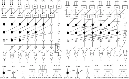
Figure 1(a) and Figure 1(b) represent 8 bit Ladner Fischer and Kogge Stone structure
of PPA respectively. Figure 1(c) represents the basic cells that are used in the
construc-tion of PPA.
For the design of large word length adders the concept of sparse is used [24]. In
sparse PPA, instead of generating carry for every bit, it generates the carry for every kth
bit therefore it is called sparse-k parallel prefix adder. Figure 2(a) represents a simple 16-bit sparse-4 PPA as shown below.
Figure 2(b) shows carry select adder block which is used in sparse-4 PPA. This
computes two sets of sum assuming carry equal to one and zero, select the resultant sum based on the carry which come from prefix network. By applying carry select ad-der in sparse PPA, routing problem is eliminated and area decreases effectively.
3. Modulo 2
n− 3 Adder
The generalized formula for modulo 2n − 3 adder is described as [20]:
(
)
if 2modulo 2 3
3 if 2
n n
n
A B A B A B
A B A B
+ + <
+ − =
+ + + ≥
(7)
The above expression for modulo 2n − 3 adder has double representation for {0, 1
and 2} with the last three numbers that are 2n − 3, 2n − 2, 2n − 1.
Unlike the modulo 2n − 1 adder, here we have to add the end around carry to the
G0,P0,H0
A0 B0 A1 B1 A2 B2 A6 B6 A5 B5 A4 B4 A3 B3 A7 B7
S7 S6 S5 S4 S3 S2 S1 S0
H7 H6 H5 H4 H3 H2 H1
G0,P0,H0
G0,P0,H0
G0,P0,H0
G0,P0,H0
G0,P0,H0
G0,P0,H0
G0,P0,H0
H0 0 Cout
G0,P0,H0
A0 B0 A1 B1 A2 B2
A6 B6 A5 B5 A4 B4 A3 B3 A7 B7
S7 S6 S5 S4 S3 S2 S1 S0
H7 H6 H5 H4 H3 H2 H1
G0,P0,H0
G0,P0,H0
G0,P0,H0
G0,P0,H0
G0,P0,H0
G0,P0,H0
G0,P0,H0
H0 0 Cout
(a) (b)
(Gi, Pi)
Gj
(Gi+Pi.Gj)
(Gi, Pi)
(Gj,Pj)
(Gi+Pi.Gj , Pi.Pj)
(Gi , Pi)
(Gi ,Pi)
PGH Ai Bi
Ai+Bi Ai.Bi Ai⊕Bi
[image:4.595.40.547.64.544.2](c)
Figure 1. 8-bit parallel prefix adder. (a) Ladner FISCHER [23], (b) Kogge Stone [22], (c) The basic cells used in PPA.
1 2 2 1 0
1 2 2 1 0
n n
n n
A A A A A B B B B B e e
− −
− −
Figure 3 describes that the carry generated in position zero enters in to next bit that
is position one which already contains EAC. In worst case the carry bypasses from po-sition two to next popo-sition. This problem can be eliminated by using carry save prepro-cessing stage [20] as shown in Figure 4.
A7 B7 A6 B6 A5 B5 A4 B4
G7, P7, H7, G6, P6,H6, G5, P5,H5, G4, P4,H4
A3 B3 A2 B2 A1 B1 A0 B0
S3 S2 S1 S0
G3, P3,H3, G2, P2,H2, G1, P1,H1, G0, P0 ,H0,
4-bit carry select adder
4-bit carry select adder
S7 S6 S5 S4
A15 B15 A14 B14 A13 B13 A12 B12
G, P, H, G, P,H, G, P,H, G, P,H
A11 B11 A10 B10 A9 B9 A8 B8
S3 S2 S1 S0
G11,P11,H11, G10,P10,H10, G9, P9,H9, G8, P8 ,H8,
4-bit carry select adder
4-bit carry select adder
S7 S6 S5 S4
cout
cin
(a)
1 0 1 0
1 0
H3
P2 G2
H1 H2
P1 G1 P0 G0
H0
S3 S2 S1 S0
[image:5.595.46.537.75.682.2](b)
Figure 3. Two stage modulo 2n − 3 adder [21].
Figure 4. Modulo (2n − 3) EAC addition using carry-save processing.
output of Ai and Bi. Gn′−1:0 represents end around carry for the next stage.
The alternative approach has been presented for modulo adder using PPA structures
[20]. It had given that ith carry expression in the case of modulo 2n − 3 adder is as fol-lows:
1:0 1:0 1:, 2 1
i i i n i
C =G− +P−′ G′− ≤ ≤ −i n (8)
where,
1 0
1:0 1:2 , 1:2 1 2 2
i i i i i
P′− =P− ⋅ ⋅P P′ ′ P− =P− ⋅P− P
1: 1:
n i n i n
[image:6.595.224.521.325.540.2]1 0 n1:0 C =u ⋅G′−
The sum expression for bit position one is
1 1 1 1 0 n1:0 1 n1:0 1 0 n1:0
S =H ⊕C =H ⊕u ⋅G′− =H G′− +H ⊕u ⋅G′− (9)
From above expression, the carries can be calculated by propagate and generate bits.
Figure 5(a) shows modulo 8
2 −3 regular parallel prefix (RPP) adder structure [20].
The RPP is differing with modulo 8
2 −1 having half carry-save stage for preprocessing,
one bit in “zero” position before enforcing the EAC and two carries enter into the
posi-tion “one” after EAC enforcement. Figure 5(b) represents modulo 8
2 −3 total
paral-lel prefix (TPP) adder structure [20]. TPP is same as RPP. The only difference is that we
have c1=Gn′−1:0u0 one gate more delay than other carries. The sum S1 is implemented
with the help of multiplexer taking Gn′−1:0 as selection line shown in Figure 5(b). For
the rest of bits the sum expression calculated using exclusive-OR gate.
The delay offered by RPP adder structure is more as compared to TPP adder struc-ture due to extra prefix level. The TPP strucstruc-ture has a disadvantage of routing complex-ity as well as excessive area problem as the bit length of adder increases.
4. Sparse Modulo 2
n− 3 Adder
In this segment, we proposed modulo 2n − 3 adder by utilizing the concept of integer
HA HA HA HA HA HA HA HA
A0 B0
A1 B1
A2 B2
A6 B6 A5 B5 A4 B4 A3 B3
A7 B7
P’GH
PGH PGH
PGH PGH
PGH PG’H
S7 S6 S5 S4 S3 S2 S1 S0 C0 C1 C2 C3 C4 C5 C6 C7
H7 H6 H5 H4 H3 H2 H1
u0 v1 v2 v3 v4 v5 v6 v7 v8 u1 u2 u3 u4 u5 u6 u7 P’GH PG’H HA
u1 v1 u0
u1+v1+u 0
u1.v1u1⊕v1 un-1+vn-1un-1.vn-1+vnun-1⊕vn-1
Ai.Bi Ai⊕Bi
(Gi , Pi)
Gj
(Gi+Pi.Gj) (Gi , Pi)
(Gj,Pj)
(Gi , Pi)
(Gi, Pi) (Gi+Pi.Gj , Pi.Pj)
vn un-1 vn-1 Ai Bi
HA HA HA HA HA HA HA HA
A0 B0
A1 B1
A2 B2
A6 B6 A5 B5 A4 B4 A3 B3
A7 B7
P’GH
PGH PGH
PGH PGH
PGH PG’H
S7 S6 S5 S4 S3 S2 S1
S0 C0 C1 C2 C3 C4 C5 C6 C7
H7 H6 H5 H4 H3 H2
H1 u0 v1 v2 v3 v4 v5 v6 v7 v8 u1 u2 u3 u4 u5 u6 u7 P’GH PG’H HA
u1 v1 u0
u1+v1+u 0
u1.v1u1⊕v1 un-1+vn-1un-1.vn-1+vnun-1⊕vn-1
Ai.Bi Ai⊕Bi
(Gi , Pi)
Gj
(Gi+Pi.Gj) (Gi , Pi)
(Gj,Pj)
(Gi , Pi)
(Gi, Pi) (Gi+Pi.Gj , Pi.Pj)
vn un-1 vn-1 Ai Bi
[image:7.595.45.550.374.683.2]0 1 H1
sparse-4 PPA in which the same carry select adder, used to implement sparse modulo 2n − 3 adder. In sparse-4, the carry is generated for every 4th bit. We are using carry se-lect adder for modulo operation so we are required to show that the rest of carries are associated with available ones.
From the general carry expression given in Equation (8)
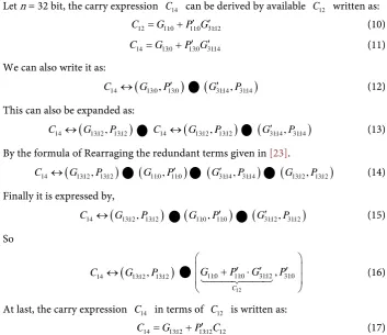
Let n = 32 bit, the carry expression C14 can be derived by available C12 written as: 12 11:0 11:0 31:12
C =G +P G′ ′ (10)
14 13:0 13:0 31:14
C =G +P G′ ′ (11)
We can also write it as:
(
)
14 13:0, 13:0
C ↔ G P′
(
G31:14′ ,P31:14)
(12)This can also be expanded as:
(
)
14 13:12, 13:12
C ↔ G P C14 ↔
(
G13:12,P13:12)
(
G31:14′ ,P31:14)
(13)By the formula of Rearraging the redundant terms given in [23].
(
)
14 13:12, 13:12
C ↔ G P
(
G11:0,P11:0′)
(
G31:14′ ,P31:14)
(
G13:12,P13:12)
(14)Finally it is expressed by,
(
)
14 13:12, 13:12
C ↔ G P
(
G11:0,P11:0′)
(
G31:12′ ,P31:12)
(15)So
(
)
14 13:12, 13:12
C ↔ G P
12
11:0 11:0 31:12, 31:0 C
G P G P
+ ′ ⋅ ′ ′
(16)
At last, the carry expression C14 in terms of C12 is written as: 14 13:12 13:12 12
C =G +P′ C (17)
From above expression we conclude that this relation is quite similar to integer adder.
Therefore we can directly use carry select block Figure 2(b) of sparse integer adder for
performing modulo operation. But the main problem is the carry expression given in Equation (8) which is defined for 2≤ ≤ −i n 1. The carry equation for C1 is quite dif-
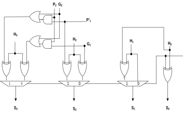
[image:8.595.200.554.150.455.2]ferent so the modification of carry select block is needed for first four bits of modulo 2n − 3 adder, it is based on carry C1 given in Equation (9).
Figure 6 is similar to carry select block of Figure 2(b) except at sum position S1. The
Figure 6 is used only for first four bits of sparse-4 modulo 2n − 3 adder. The remaining
bits uses carry select block of Figure 2(b) for implementation of sparse modulo (2n − 3) adder.
This sparse-4 modulo 2n − 3 adder has double representation for {0,1,2} with 2n − 3,
2n − 2, 2n − 1, so there are six pairs of combinations in which two pairs has tendency to
produce wrong addition result. The solution for this problem is explained in [20] and
[21]; these explanations still exist for proposed adder.
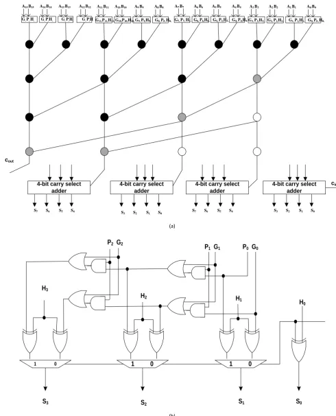
Figure 7 represents the proposed 32 bit sparse modulo 2n − 3 Adder having lesser
1 0 1 0
1 0
H3
P2 G2
H1
H2
P’1
H0
S3 S2 S1 S0
[image:9.595.194.550.74.293.2] [image:9.595.100.542.329.684.2]G1
Figure 6. Carry select block for modulo 2n− 3 adder only for first 4 bits.
HA HA
HA HA HA HA HA HA
HA HA
HA HA HA HA HA
HA
PGH PGH PGH PGH PGH PGH PGH PGH
PGH PGH PGH PGH PGH PGH PGH
A0B0
B1
A1
A3 B3 A2 B2
A5 B5 A4 B4
A6 B6
A7 B7
A28 B28 A27 B27
A30 B30 A29 B29
A31 B31 A26 B26 A25 B25 A24 B24
u0
v1
u1
v2
u2
v3
u5
v6
u4
v5
u3
v4
u6
v7
u7
v8
u24
v25
u25
v26
u26
v27
u27
v28
u28
v29
u29
v30
u30
v31
u31
v32
Modified 4-bit Carry Select Adder for modulo
2n
-3 4-bit Carry Select Adder
4-bit Carry Select Adder 4-bit Carry Select Adder
S3 S2 S1 S0 S7 S6 S5 S4
S11 S10 S9 S8 S31 S30 S29 S28
5. Performance Analysis and Comparison
The theoretical area and delay analysis is explained in terms of area (∆a) and delay (∆g) of basic 2-input gates. From the concept of unit gate model, basic 2-input AND, OR, NAND, NOR are assumed as single unit gate (∆a, ∆g), whereas exclusive-OR &
exclu-sive-NOR and assumed to be double unit gate (2∆a, 2∆g) [15]. The area and delay of
Inverters and buffers are not taken into account in unit gate model.
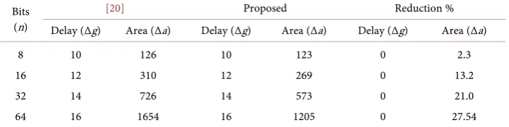
The delay offered by proposed sparse modulo 2n − 3 adder is same as [20]. Table 1
shows the estimated gate delay and gate area of proposed adder as function of bit length n.
Table 2 shows the unit gate delays and unit gate areas for different values of n of
proposed adder and also shows the percentage reduction in area in comparison with
[20].
The percentage reduction in area increases as the number of bit length increases. We have also elaborated proposed work with HDL code written on Xilinx 14.7 and verified for correctness using simulation tests. Number of lookup table (LUTs) count is given in
Table 3 for n = 8 which measures the area utilization for proposed adder.
6. Conclusion
In this paper, we have proposed an area efficient sparse modulo 2n − 3 adder which
[image:10.595.192.554.440.510.2]plays an important role in verity of computer applications. The efficiency in term of area of proposed adder is explained by using the concept of unit gate model. For dif-ferent value of n (=8, 16, 32, 64), the percentage area reduction is (=2.3, 13.2, 21, 27.54)
Table 1. Adders unit gate area and delay estimations.
Adder Delay (∆g) Area (∆a)
[20] 2 log( )n +4 3 logn ( )n +8n−10
Proposed 2 log( )n +4 29 3 log( ) 11
2 4
[image:10.595.194.555.545.635.2]n n n+ −
Table 2. Delay and area for different bit length.
Bits (n)
[20] Proposed Reduction % Delay (∆g) Area (∆a) Delay (∆g) Area (∆a) Delay (∆g) Area (∆a) 8
16 32 64
10 12 14 16
126 310 726 1654
10 12 14 16
123 269 573 1205
0 0 0 0
2.3 13.2 21.0 27.54
Table 3. LUT count for n = 8.
[20] Proposed Sparse Adder % Reduction in LUT Count
respectively with same delay. Simulation results show that the area of proposed adder has been reduced by 34% in term of LUT count for n = 8. Therefore, it is observed that, the presented modulo adder offers less area in performing the addition for larger word length input and also reduces the routing complexity in comparison with the previously reported adder.
References
[1] Ma, S., Hu, J.H., Zhang, L. and Xiang, L. (2008) An Efficient RNS Parity Checker for Mod-uli Set and Its Applications. Science in China, Series F: Information Sciences, 51, 1563- 1571.
[2] Garner, H.L. (1959) The Residue Number System IRE. Transactions on Electronic
Com-puters, 8, 140-147. http://dx.doi.org/10.1109/TEC.1959.5219515
[3] Garai, P. and Dutta, C.B. (2014) RNS Based Reconfigurable Processor for High Speed Signal Processing. TENCON 2014—2014 IEEE Region 10 Conference, Bangkok, 22-25 October 2014, 1-6.
[4] Di Claudio, E. D., Piazza, F. and Orlandi, G. (1995) Fast Combinatorial RNS Processors for DSP Applications. IEEE Transactions on Computers, 44, 624-633.
http://dx.doi.org/10.1109/12.381948
[5] Chang, C.H., Molahosseini, A.S., Zarandi, A.A.E. and Tay, T.F. (2015) Residue Number Systems: A New Paradigm to Datapath Optimization for Low-Power and High-Perfor- mance Digital Signal Processing Applications. IEEE Circuits and Systems Magazine, 15, 26- 44.
[6] Kurokawa, T., Payne, J. and Lee, S. (1980) Error Analysis of Recursive Digital Filters Im-plemented with Logarithmic Number Systems. IEEE Transactions on Acoustics, Speech,
and Signal Processing, 28, 706-715. http://dx.doi.org/10.1109/TASSP.1980.1163466
[7] Krishnan, R., Jullien, G. and Miller, W. (1985) Complex Digital Signal Processing Using Quadratic Residue Number Systems. IEEE International Conference on Acoustics, Speech,
and Signal Processing, 764-767.
[8] Schinianakis, D.M., Kakarountas, A.P. and Stouraitis, T. (2006) A New Approach to Elliptic Curve Cryptography: An RNS Architecture. MELECON 2006—2006 IEEE Mediterranean
Electrotechnical Conference, Malaga, 16-19 May 2006, 1241-1245.
[9] Safari, A., Niras, C.V. and Kong, Y. (2016) Power-Performance Enhancement of Two-Di- mensional RNS-Based Dwt Image Processor Using Static Voltage Scaling. Integration, 53, 145-156.
[10] Taleshmekaeil, D.K. and Mousavi, A. (2010) The Use of Residue Number System for Im-proving the Digital Image Processing. IEEE 10th International Conference on Signal
Processing Proceedings, Beijing, 24-28 October 2010, 775-780.
[11] Taleshmekaeil, D.K., Mohamamdzadeh, H. and Mousavi, A. (2011) Using Residue Number System for Edge Detection in Digital Images Processing. 2011 IEEE 3rd International
Con-ference on Communication Software and Networks (ICCSN), Xi’an, 27-29 May 2011, 249-
253.
[12] Etzel, M. and Jenkins, W. (1980) Redundant Residue Number Systems for Error Detection and Correction in Digital Filters. IEEE Transactions on Acoustics, Speech, and Signal
Processing,28, 538-545. http://dx.doi.org/10.1109/TASSP.1980.1163442
2008, 192-194. http://dx.doi.org/10.1109/iolts.2008.14
[14] Yang, L.-L. and Hanzo, L. (2002) A Residue Number System Based Parallel Communica-tion Scheme Using Orthogonal Signaling. I. System Outline. IEEE Transactions on
Vehicu-lar Technology, 51, 1534-1546. http://dx.doi.org/10.1109/TVT.2002.804850
[15] Zimmermann, R. (1999) Efficient VLSI Implementation of Modulo (2n ± 1) Addition and Multiplication. 14th IEEE Symposium on Computer Arithmetic, Adelaide, 14-16 April 1999, 158-167.
[16] Chang, C.H. and Low, J.Y.S. (2011) Simple Fast and Exact RNS Scaler for the Three-Moduli Set 2n − 1, 2n, 2n + 1. IEEE Transactions on Circuits and Systems I: Regular Papers, 58, 2686-2697. http://dx.doi.org/10.1109/TCSI.2011.2142950
[17] Ananda Mohan, P.V. (2008) New Reverse Converters for the Moduli Set {2n− 3,2n− 1,2n+ 1,2n + 3}. International Journal of Electronics and Communications, 62, 643-658. http://dx.doi.org/10.1016/j.aeue.2007.08.008
[18] Kalampoukas, L., et al. (2000) High-Speed Parallel-Prefix Modulo 2n− 1 Adders. IEEE
Transactions on Computers, 49, 673-680.
[19] Vergos, H.T. and Dimitrakopoulos, G. (2012) On Modulo 2n + 1 Adder Design. IEEE
Transactions on Computers, 61, 173-186.
[20] Jaberipur, G. and Langroudi, S.H.F. (2015) (4 + 2logn)∆G Parallel Prefix Modulo-2n− 3 Adder via Double Representation of Residues in [0, 2]. IEEE Transactions on Circuits and
Systems II: Express Briefs, 62, 583-587. http://dx.doi.org/10.1109/TCSII.2015.2407772
[21] Fatemi, H. and Jaberipur, G. (2014) Double {0, 1, 2} Representation Modulo-(2n − 3) Ad-ders. IWSSIP Proceedings, Dubrovnik, 12-15 May 2014, 119-122.
[22] Kogge, P.M. and Stone, H.S. (1973) A Parallel Algorithm for the Efficient Solution of a General Class of Recurrence Equations. IEEE Transactions on Computers, 22, 786-793. http://dx.doi.org/10.1109/TC.1973.5009159
[23] Ladner, R.E. and Fischer, M.J. (1980) Parallel Prefix Computation.Journal of the ACM, 27, 831-838. http://dx.doi.org/10.1145/322217.322232
[24] Mathew, S., Anders, M., Krishnamurthy, R. and Borkar, S. (2002) A 4 GHz 130 nm Address Generation Unit with 32-Bit Sparse-Tree Adder Core. VLSI Circuits Digest of Technical
Papers, Honolulu, 13-15 June 2002, 126-127.
Submit or recommend next manuscript to SCIRP and we will provide best service for you:
Accepting pre-submission inquiries through Email, Facebook, LinkedIn, Twitter, etc. A wide selection of journals (inclusive of 9 subjects, more than 200 journals)
Providing 24-hour high-quality service User-friendly online submission system Fair and swift peer-review system
Efficient typesetting and proofreading procedure
Display of the result of downloads and visits, as well as the number of cited articles Maximum dissemination of your research work
Submit your manuscript at: http://papersubmission.scirp.org/
![Figure 1. 8-bit parallel prefix adder. (a) Ladner FISCHER [23], (b) Kogge Stone [22], (c) The basic cells used in PPA](https://thumb-us.123doks.com/thumbv2/123dok_us/7830139.732663/4.595.40.547.64.544/figure-parallel-prefix-adder-ladner-fischer-kogge-stone.webp)
![Figure 3. Two stage modulo 2n − 3 adder [21].](https://thumb-us.123doks.com/thumbv2/123dok_us/7830139.732663/6.595.224.521.325.540/figure-two-stage-modulo-n-adder.webp)