The effect of substrate geometry and surface orientation on the
fi
lm
structure of DLC deposited using PECVD
N. Nelson
a, R.T. Rakowski
a, J. Franks
b, P. Woolliams
c, P. Weaver
c, B.J. Jones
a,d,⁎
aBrunel University, Kingston Lane, Uxbridge, Middlesex. UB8 3PH, UK
bRenishaw Advanced Materials, Brunel University, Kingston Lane, Uxbridge, Middlesex. UB8 3PH, UK c
National Physical Laboratory, Hampton Road, Teddington, Middlesex. TW11 0LW, UK
d
University of Huddersfield, Queensgate, Huddersfield, West Yorkshire. HD1 3DH, UK
a b s t r a c t
a r t i c l e i n f o
Article history:
Received 17 August 2013
Accepted in revised form 31 May 2014 Available online 9 June 2014
Keywords:
Diamond-like carbon Surface topography Microstructure Plasma CVD
Potential applications of diamond-like carbon (DLC) coatings range from precision tools and biomedical implants to micro mechanical devices and engine components. Where uniform coatings are required on substrates with com-plex geometries, plasma enhanced chemical vapour deposition (PECVD) is often a preferred deposition method. As a non-line of sight process, the geometry of the substrate is often considered negligible. For this reason analysis of PECVD coatings, such as amorphous carbon, has mostly been concerned with reactor deposition variables, such as bias voltage, pressure and gas ratios. Samples are therefore usually prepared and positioned to minimise the infl u-ence of other variables. By depositing nominally similar DLCfilms on silicon samples positioned horizontally and vertically on the reactor cathode plate it was possible to examine the variations in the coating characteristics and mechanical properties that occur due to the geometry of the substrate being coated. Topographic measurements and analysis of bonding structures revealed significant heterogeneity in the coatings. Electron microscopy showed variation in surface structure as well as thickness disparities of up to 50% in the vertical sample. Atomic force micros-copy showed roughness,Ra, varied from 0.37 nm to 15.4 nm between samples. Raman spectroscopy highlighted variations in the sp2/sp3bonding ratios whilst micro wear tests demonstrated how these variations reduce the crit-ical load performance. These effects are explained in terms of the deposition mechanisms involved and are related to variation in deposition species and geometricalfield enhancements within the deposition chamber. Improved un-derstanding of these local variations will aid in the optimisation of coatings for complex substrate geometries.
© 2014 The Authors. Published by Elsevier B.V. This is an open access article under the CC BY license (http://creativecommons.org/licenses/by/3.0/).
1. Introduction
Diamond like carbon (DLC) thin films are of great interest to engineers not only because of their unique properties such as high mechanical hardness, wear resistance, low friction, chemical inertness and biocompatibility, but also due to their ability to be tailored to meet specific requirements[1–4]. These material characteristics are due to the surface structure and internal bonding, which consists of a combination of diamond-like sp3and graphite-like sp2bonds, as well
as a significant amount of hydrogen[2,5].
Many processes have been developed for the deposition of amorphous carbon materials, the deposition methods employed will usually be selected based on the desired coating properties, as different processes create subtle differences in the characteristics of deposited
films[2,4]. RF plasma enhanced chemical vapour deposition (PECVD) is a common laboratory deposition process, due to its ability to produce
a wide range of coatings over large areas at relatively low temperatures [4,5].
The benefits of PECVD come from the fact that the carbon containing plasma surrounds the substrate; it is therefore considered a non-line of sight (NLOS) process. This is unlike line of sight systems such asfiltered cathodic vacuum arc (FCVA) in which a beam of ions is directed towards the substrate. A considerable drawback, however, may be that the process cannot be used to create harder tetrahedral amorphous carbon (ta-C) coatings, due to the incorporation of hydrogen from the gaseous precursors[6].
By altering the parameters in the deposition process, the material characteristics and mechanical properties of the DLC thinfilm can be greatly modified[7–10]. It is theflexibility in the deposition process, coupled with the low temperature of the method, which allow for such a wide range of achievable coating properties. DLC deposited using the rf PECVD method therefore has widespread applications ranging from biomedical implants and electronic devices, to aerospace components and precision manufacturing applications, such as turning inserts, drill bits and milling tools[11–15]. Many of these components require a uniform coating over several surfaces at various orientations;
⁎ Corresponding author at: School of Applied Sciences, University of Huddersfield, Queensgate, Huddersfield, West Yorkshire. HD1 3DH, UK. Tel.: +44 (0)1484 473658.
E-mail address:[email protected](B.J. Jones).
http://dx.doi.org/10.1016/j.surfcoat.2014.05.066
0257-8972/© 2014 The Authors. Published by Elsevier B.V. This is an open access article under the CC BY license (http://creativecommons.org/licenses/by/3.0/).
Contents lists available atScienceDirect
Surface & Coatings Technology
any disparity in thefilm structure can have a significant negative impact on the performance and reliability of such coatings.
Researchers have investigated the effect of substrate material and how micro topographical features can alterfilm growth[12,16–18]; however, as PECVD is considered an NLOS process, larger geometrical variations of the substrate have been considered to have a negligible effect on thefilm structure[1]. Nevertheless, a previous study highlighted how small differences in substrate thickness can affect the deposition rate of DLC in a parallel plate PECVD process[19]. Simulations conducted by Waddell et al. used a dome shape to examine how slight variations in substrate geometry may affect coating thicknesses and deposition rates[20]. Furthermore, variations in DLC coatings due to substrate geometry have been examined for other deposition methods. Bobzin et al.[21]investigated substrate geometry effects in magnetron sputter ion plating by altering substrate orientation and effectively varying the ion impingement angle. Ding et al.[22]completed a detailed study re-garding the effects of substrate geometry of chromium-doped DLC, de-posited using unbalanced magnetron sputtering. The investigation revealed how coating thickness, microhardness and bonding ratios were affected by the shielding of surfaces in close proximity.
Previous work has shown that certain substrate geometries will be more difficult to coat as adjacent surfaces will be shielded from impinging ions whilst sharp edges and points will lead to a concentration of ions impacting the surface [23–26]. This article focuses on how such variations in the orientation of substrates within the PECVD reactor can affect the coating characteristics and mechanical properties, which, in many applications, may lead to reduced performance of the DLC thinfilm.
2. Experimental details
2.1. Film deposition
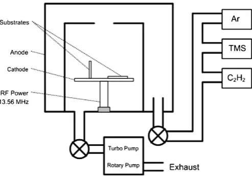
DLC coatings, formed of amorphous hydrogenated carbon top layer with a graduated amorphous silicated hydrogenated carbon interlayer, were deposited on single sided [100] silicon wafer pieces of approxi-mately 10 mm × 10 mm, and thickness 0.66 mm, using a 13.6 MHz rf PECVD process at Renishaw Advanced Materials Ltd. Silicon was chosen as it provides a smooth uniform surface and promoted good adhesion. The uniformity removes further potentialfluctuations in the coating, which may be due to slight topographical variations, ensuring that the heterogeneity measured in the samples can be attributed solely to the sample positioning in the reactor. All samples were ultrasonically cleaned in acetone for 10 min before being placed in the deposition chamber. The samples were placed horizontally and vertically on the cathode plate. The horizontal samples were simply placedflat on the plate whilst the vertical samples were clamped at the base (Fig. 1).
For the deposition process a mixture of argon, acetylene and tetramethylsilane (TMS) gas was used. The gas was introduced to the reactor through a grating at the top of the chamber and evacuated off-axis at the base below the cathode. Pre-treatment included a cleaning stage using 30 sccm of argon for 30 min at a bias of 370 V in order to clean the substrate without restructuring the surface[27]. Argonflow was then reduced to 10 sccm and TMS was set at 25 sccm for 15 min to create a silicon layer for improved adhesion[28]. The TMSflow was then halved and acetylene was introduced at 60 sccm for a further 15 min. The TMSflow was then reduced to zero and the acetylene and argon maintained at 60 sccm and 10 sccm respectively for thefinal 15 min to produce the DLC layer. The negative self bias voltage was maintained at 450 V throughout the deposition stages by altering the rf power. The rf power ranged between 150 W and 215 W and the pressure was maintained at 5 × 10⁻⁴Torr ± 1 × 10⁻⁴Torr
dur-ing deposition.
2.2. Surface characterisation
The surface structure was analysed using a Ziess Supra 35VP scanning electron microscope (SEM) and a Dimension 3100 atomic force microscope (AFM). SEM has been used to create micrographs of the sample surface, operating in high vacuum and with an accelerating voltage of 6 kV for improved surface resolution. AFM was used in tapping mode to measure the height variation of the sample surfaces. Scans were conducted using a silicon cantilever with a resonant frequency of ~ 190 kHz, a force constant of approximately 48 N/m and a nominal tip radius of 8 nm. Roughness [Ra], skewness and kurtosis of
films were calculated from the AFM data at specific points on the samples. These parameters are calculated from thefirst, third and fourth powers of the height distribution, respectively. Skewness and kurtosis reflect the symmetry of the surface and peak sharpness, respectively; further details are provided in ISO 4827: 2000 and example real surfaces and their respective measured parameters are shown in a previous study[29]. The horizontal and vertical samples were measured in 1 mm increments from edge to edge and top to the base respectively, with increased spatial frequency of sampling close to the edges. The
figures reported for each position are mean and standard deviation of measurements over four separate 10μm × 10μm areas; the quoted uncertainties therefore do not directly reflect noise error and any system-atic offset, but allow for quantitative relative comparisons and demon-stration of variability.
2.3. Film thickness
The horizontal and vertical samples were sectioned edge to edge and top to bottom respectively; the sections were then analysed using SEM and coating thicknesses were measured at specific points.
2.4. Bonding structure
Raman spectroscopy was conducted to analyse the bonding structure within the DLC coating. A Renishaw inVia Raman system was used, with 514 nm laser radiation, to compare the areas of the disordered (D) and graphitic (G) peaks. The intensity ratio I(D)/I(G) has been shown to be connected to sp2and sp3concentrations[30],
with lower ratios indicating higher sp3content. The horizontal sample
[image:2.595.36.283.554.727.2]was measured at 1 mm increments from edge to edge whilst the vertical sample was measured in 1 mm increments from the top to the bottom of the sample. The peaks werefitted using two 100% Gaussian curves; although there is no physical reason to utilise one particular curve shape, and other groups have had success with a combination of Breit–Wigner–Fano and Lornetzian functions, the consistent use of two Gaussians in this study enables comparison of peak position shift and peak ratio to that of other works studying amorphous hydrogenated carbon[30].
2.5. Microtribology tests
Teer scratch tests were conducted by the National Physical Laboratory. The friction and hardness of thefilms were measured at specific points on the samples. Measurements were conducted using a 250μm radius diamond indenter. All tests involved a 5 mm scratch, at a speed of 0.1 mm/s with a load ramp from 0.5 N to 20 N, in 30 steps. In all these tests the substrate was cleaned with an air jet before and after every scratch to remove debris that might affect the subsequent scratches. Similarly the indenter tip was wiped with alcohol to remove debris between tests. Due to the brittle nature of the substrate it was not possible to conduct scratches at the very edge of the samples. The scratches in horizontal and vertical samples were parallel to the (top) edge at approximately 2.3 mm, 4.6 mm and 6.9 mm from the edge and top respectively.
3. Results
3.1. Topography
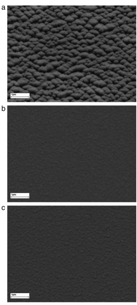
The SEM images of thefilm surface show variation in the topography with sample orientation and position within the vertically orientated sample. There is significant nodulization and ridge formation at the very top of the vertical samples, whilst the horizontal samples and lower areas of the vertical samples appeared relatively featureless (Fig. 2). AFM images also highlighted the variations in the topography of the coating as well as directionality in the surface structure (Fig. 3). The DLC near the top of the vertical sample has formed a ridged structure parallel to the top edge, whilst the vertical mid sections and horizontal sample coatings show no immediate directionality effects in the coating structure. AFM measurements confirmed that roughness, Ra, values varied significantly between the samples. The horizontal
samples had the lowest roughness of 0.37 nm ± 0.03 nm whilst the vertical samples had a roughness of 15.4 nm ± 2.4 nm at the top, which decreases smoothly over 2 mm, approaching a minimum of 1.29 nm ± 0.09 nm at the middle of the sample (Fig. 4). Skewness and kurtosis measurements also highlight the variation in the surface structure in the top 1 mm of the vertical sample (Fig. 4).
3.2. Coating thickness
SEM analysis of the sectioned samples showed that the top of the vertical sample had a nodular growth pattern throughout the silicon and carbon layers, compared to the horizontal sample which had a much more uniform coating with clear transition lines between layers (Fig. 5). Measurements of the coatings show that the thickness of the horizontal sample was constant over the sample at 1.69 μm ± 0.04μm. Thefilms on the vertical samples, in contrast, showed large variation in thickness. At the base of the sample the coating thickness was 1.2μm ± 0.1μm, increasing smoothly to 1.8μm ± 0.2μm at the top (Fig. 6).
3.3. Raman spectroscopy
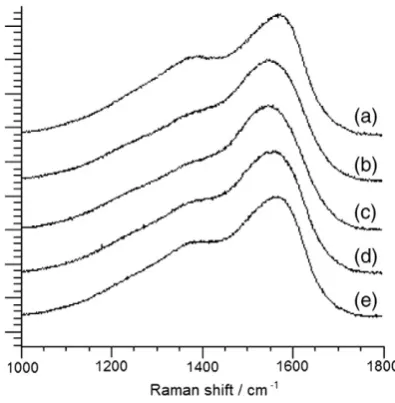
It can be seen from the Raman spectra of the vertical sample that the G peak, around 1580–1600 cm−1, shifts to higher wavenumber and the
height of the D peak at around 1350 cm−1is increased as the sample
extremities are approached (Fig. 7). Analysis of the I(D)/I(G) ratios of the samples indicated that the horizontal sample had a higher average sp3content compared to the vertical sample; I(D)/I(G) area ratios
were 1.07 ± 0.02 for the horizontal sample compared to 1.67 ± 0.08 in the middle of the vertical sample. In the top 2 mm of the vertical sample the ratio increased up to 2.63 ± 0.09 (Fig. 8). It was also noted that accurate measurements were not possible within the top 1 mm of the vertical sample due to significant amounts of background noise caused by the rougher surface. It has been shown that such variation
corresponds to an sp3concentration of 40% in the horizontal sample
and between 25% and 30% in the vertical sample[30].
3.4. Friction and critical load
[image:3.595.323.548.45.545.2]Scratch testing determined the failure load of thefilm for the horizontal sample to be on average 8.0 N ± 0.6 N. The failure load of the vertical sample was found to be roughly half that value at 4.0 N ± 0.1 N. Friction measurements before failure showed the horizontal sam-ple to have the lowest friction coefficient of 0.08 ± 0.01. The vertical sample was marginally better than the bare silicon at 0.13 ± 0.01 com-pared to 0.16 ± 0.01. Measurements of friction and failure load showed little variation within each sample.
Fig. 3.AFM images of surface topography 1μm scan size (a) top of the vertical sample, (b) middle of the vertical sample and (c) middle of the horizontal sample. Note the differences in vertical scale.
[image:4.595.311.535.49.343.2]Fig. 4.Graphs showing roughness, skewness and kurtosis, against distance from top/edge of horizontal and vertical samples. Lines are a guide to the eye.
[image:4.595.316.540.395.718.2]4. Discussion
At a macro level a PECVD produced DLCfilm is often conformal to the substrate topography; however, the growth of DLC will usually lead to a microstructure which has a nodular formation[27,31–33]. The dominant growth mechanisms and resultant structure will vary depending on the substrate[12,18,27]as well as the process parameters[34–36]. The use of smooth silicon as a model surface minimises the effects of substrate materials and texture in variation of the DLC structure. Maheswaren et al.[37]used AFM to show that in this case, the DLC deposited on Si wafer nucleates in individual islands; these islands grow before combining to form a continuous coating. Other works[27,33,35]discuss the effects of ion energy and interaction with the substrate and conse-quently balance of growth mechanisms, argon sputtering and hydrogen etching during thefilm growth.
The observed variations infilm roughness between the horizontal and vertical samples, as well as the deviations within the vertical sample, can be understood by considering the deposition mechanisms associated with the PECVD process. The variations are likely to be as a
result of a number of geometrical differences in the sample. Firstly, the distance from the cathode plate will have an effect on the vertical sample. Secondly, the orientation of the substrate surface relative to the cathode plate, and hence direction of the ions varies between the horizontal and vertical samples andfinally the protruding top edge of the vertical sample will lead to a concentration of impinging ions whilst the lower half will be shielded.
The distribution of ion and radical species in the plasma is heteroge-neous and will be affected by precursor gases, gas pressure, reactor design such as gas influx and exhaust positioning, as well as geometry of the substrate and cathode. This has been highlighted by computationalfluid dynamics[38,39]and the modelling in some cases partially compared with optical spectroscopy and mass spectrometry data[39]. Although based on different geometries and precursor mixes, and where available with only approximate match to experimental data, the scale over which variation occurs is comparable to the size of samples in this study. It may therefore be supposed that the height of the vertical sample will mean a variation in the chemistry of the species impinging on the substrate, for example, the balance of CH3, C, and H, resulting in changes
to the growth processes. This variation in impinging species has previously been shown to affect the resultantfilm composition, structure and growth rate[18,33–35,39].
At the top/edge of the substrate more carbon ions are impacting a smaller surface area with a much greater impact angle range. The subplantation model of DLC growth describes how the ions impact the surface displacing other atoms before coming to rest[5]. Ions of energies below the penetration threshold have been shown to bond at the surface of thefilm forming a more uneven and less dense coating containing higher amounts of sp2bonding. Ions with energies exceeding the penetration threshold will travel deeper into the deposited layer before relaxing, dissipating energy to surrounding atoms, maintaining a much smoother surface and an increase in sp3bonds. For efficient
[image:5.595.45.293.52.240.2]subplantation the ions should also be travelling normal to the substrate surface, this ensures the majority of their energy is used to penetrate the surface[40]. On the vertical sample and particularly at the top edge, as the direction of the impinging ion deviates from the normal line, more total energy will be required for the ion to reach the same depth; as the proportion of momentum perpendicular to the surface decreases, the likelihood of subplantation decreases and the surface diffusion may increase. This has been observed in works studying the angle of substrate in line-of-sightfiltered cathodic vacuum arc (FCVA) deposited DLC[41,42]. In the rf-PECVD system the plasma forms a sheath layer between the bulk plasma and the substrate. The geometry and electrical conductivity of the sample will affect the surrounding plasma and
Fig. 6.Coating thickness relative to edge/base of the horizontal and vertical samples derived from SEM images.
[image:5.595.312.560.53.242.2]Fig. 7.Raman spectra of the vertically positioned sample, representing areas at a) 1 mm, b) 3 mm, c) 6 mm, d) 8 mm and e) 10 mm from the sample top edge.
Fig. 8.ID/IGarea ratios fromfitting of Raman spectra of vertical and horizontal samples.
[image:5.595.67.265.519.721.2]sheath formation. Sharp protruding edges will create a distortion or curvature of the sheath boundary, which determines the path of ions towards the substrate/cathode. The top of the vertical sample will there-fore be subjected to a concentration of impinging ions; further down the sample thefilm deposition will be from lower energy ions at a more oblique angle. The concentration and dispersion of impinging ions can also be considered in terms of ionflux. The sharp edges and heterogeneity of species distribution lead to a greaterflux which in turn increases depo-sition rate. The increasedflux, however, will also produce more inelastic collisions reducing the ion impact energies resulting in reduced coating quality. The extent and shape of the sheath boundary curvature, and subsequent effects on thefilm, will be dependent on variables such as the gas pressure and applied power and will be increased as the sharpness of the substrate edge increases and will reduce with a less sharp or thicker sample. Similar effects have been observed on DLC coating of narrow tubes[43]. The irregular growth on the vertical sample may therefore be attributed to the combination of these effects, causing lower effective energies of ions impacting the surface, meaning that fewer ions can penetrate the material creating more disruption in the coating surface and leading to the increased roughness observed by AFM and the increase in sp2bonding fraction observed by Raman
spectroscopy. The effects of hydrogen etching and argon sputtering duringfilm growth are also likely to be affected through similar processes, leading to an increase in surface roughening[1,5,33].
These variations in the coating topography and structure have in turn had a great effect on the mechanical properties. The large difference in the critical load values between the horizontal and vertical samples are related to the differences in the texture and sp3
concentra-tion of the coatings. The increased roughness of the vertical sample leads to increased friction coefficients and, along with the reduced sp3
content, which may be linked to a softerfilm, leads to a lowered critical load value compared to the horizontal sample. Although there is signif-icant variation of sp3content and surface roughness on the vertically
positioned sample, little variation was seen among the microtribology results; this is related to the positioning of the test scratches in the mid-dle section of the sample, due to the brittle substrate, and does not
re-flect the full variation of the coating properties. It is expected that the coating at the very edge would have further reduced tribological perfor-mance in comparison, related to the topological differences. For some samples of complex geometries, a rotating carousel system, as opposed to a static substrate, may reduce the orientation dependent variation of thefilm structure and quality.
5. Conclusions
The investigation has highlighted that substrate geometries have the potential to significantly alter coating characteristics of DLC deposited using the PECVD method. The surface structure varied greatly between the vertical and horizontal samples as well as between different areas on the vertical sample. The mean value of roughness, Ra, was a
maximum at the top of the vertical sample at 15.4 nm± 2.4 nm de-creasing smoothly over 2 mm, approaching a minimum of 1.29 nm ± 0.09 nm at the middle of the sample, significantly higher than the roughness of the sample coated in a horizontal position, which was 0.37 nm ± 0.03 nm, varying little over the sample.
Analysis of the bonding structure showed the vertical sample to have lower sp3content than the horizontal, with the top of the vertical
sample having the least sp3content, 10% less than the horizontal. Teer
scratch tests revealed that these variations can increase the friction coefficient from 0.08 to 0.13 whilst reducing the critical load of the
film from 8.0 N to 4.0 N.
Sharp edges on the substrate act to concentrate the impinging ions, which lead to an increase in deposition rate, whilst the region distal from the tip has a reduced amount of impinging ions which decreases the deposition rate andfinalfilm thickness. Plasma concentrations and reduced effective ion energy efficiency mean that fewer impinging
ions can penetrate the surface. This in turn leads to rougher coatings with higher sp2fraction and reduced tribological performance.
It has been shown that in a PECVD system, variations in substrate orientation can lead to very large differences in the characteristics and mechanical properties of the DLC coating.
Acknowledgements
This work was partially funded through the Technology Strategy Board grant BD266E and with support of the Engineering and Physical Sciences Research Council. We would like to acknowledge members of the SEEM consortium at Renishaw, NPL, and Brunel and Bristol Univer-sities for helpful discussions and strategy planning.
References
[1] A. Grill, Diam. Relat. Mater. 8 (2–5) (1999) 428–434.
[2] Y. Lifshitz, Diam. Relat. Mater. 8 (8–9) (1999) 1659–1676.
[3] A. Erdemir, C. Donnet, J. Phys. D. Appl. Phys. 39 (18) (2006) R311–R327.
[4] S.V. Hainsworth, N.J. Uhure, Int. Mater. Rev. 52 (3) (2007) 153–174.
[5] J. Robertson, Mater. Sci. Eng. R. Rep. 37 (4–6) (2002) 129–281.
[6] F. Cerny, V. Jech, S. Konvickova, J. Suchanek, Appl. Surf. Sci. 256 (3) (2009) S22–S25.
[7] A.A. Ogwu, R.W. Lamberton, P.D. Maguire, J.A. McLaughlin, J Phys. D 32 (9) (1999) 981.
[8] W.S. Choi, J. Heo, I. Chung, B. Hong, Thin Solid Films 475 (1–2) (2005) 287–290.
[9] A. Erdemir, O.L. Eryilmaz, I.B. Nilufer, G.R. Fenske, Diam. Relat. Mater. 9 (3-6) (2000) 632–637.
[10]Y.T. Kim, S.M. Cho, W.S. Choi, B. Hong, D.H. Yoon, Surf. Coat. Technol. 169 (2003) 291–294.
[11] V.P. Astakhov, Int. J. Mach. Tools Manuf. 44 (6) (2004) 637–647.
[12] S. Podgoric, B.J. Jones, R. Bulpett, G. Troisi, J. Franks, Wear 267 (2009) 996.
[13] B. Jones, T. Anson, Mater. World 16 (8) (2008) 24.
[14] G. Byrne, D. Dornfeld, B. Denkena, CIRP Ann. Manuf. Technol. 52 (2) (2003) 483–507.
[15] B.J. Jones, A. Mahendran, A.W. Anson, A.J. Reynolds, R. Bulpett, J. Franks, Diam. Relat. Mater. 19 (2010) 685–689.
[16]M.C. Salvadori, D.R. Martins, M. Cattani, Surf. Coat. Technol. 200 (16–17) (2006) 5119–5122.
[17] M. Zhong, C. Zhang, J. Luo, Appl. Surf. Sci. 254 (21) (2008) 6742–6748.
[18] B.J. Jones, J.J. Ojeda, Surf. Interface Anal. 44 (2012) 1187–1192.
[19]O.V. Balachova, M.A.R. Alves, J.W. Swart, E.S. Braga, L. Cescato, J. Appl. Phys. 85 (6) (1999) 3345–3347.
[20] E. Waddell, D. Gibson, L. Lin, F. Xiuhua, Modelling and optimization offilm thickness variation for plasma enhanced chemical vapour deposition processes, Advances in Optical Thin Films Iv, 81682011. 81681I.
[21]K. Bobzin, N. Bagcivan, N. Goebbels, K. Yilmaz, Plasma Process. Polym. 6 (2009) S425–S428.
[22] X. Ding, X.T. Zeng, Z.Q. Hu, Thin Solid Films 461 (2) (2004) 282–287.
[23] P. Chabert, J. Phys. D. Appl. Phys. 40 (3) (2007) R63–R73.
[24] N. de Freitas Daudt, J.C. Pereira Barbosa, D.C. Braz, M.B. Pereira, C. Alves Junior, 12th High-Tech Plasma Processes Conference [Htpp-12], 406, 2012, p. 012021.
[25]M.A. Neto, A.J.S. Fernandes, R.F. Silva, F.M. Costa, Diamond Relat. Mater. 17 (4-5) (2008) 440–445.
[26] X.C. Zhang, B.S. Xu, H.D. Wang, Y.X. Wu, Thin Solid Films 515 (4) (2006) 2251–2256 (2006).
[27] B.J. Jones, L. Anguilano, J.J. Ojeda, Diam. Relat. Mater. 20 (7) (2011) 1030–1035.
[28]M. Zolgharni, B.J. Jones, R. Bulpett, A.W. Anson, J. Franks, Diam. Relat. Mater. 17 (7–10) (2008) 1733–1737.
[29] B.J. Jones, R. Downham, V.G. Sears, Surf. Interface Anal. 42 (2010) 438–442.
[30] A.C. Ferrari, J. Robertson, Phys. Rev. B 61 (20) (2000) 14095–14107.
[31]A.P. Mousinho, R.D. Mansano, M.C. Salvadori, Surf. Coat. Technol. 203 (9) (2009) 1193–1198.
[32] Z. Sun, J. Non-Cryst. Solids 261 (1–3) (2000) 211–217.
[33] X.L. Peng, Z.H. Barber, T.W. Clyne, Surf. Coat. Technol. 138 (1) (2001) 23–32.
[34] M. Ouchabane, H. Salah, M. Herrmann, N. Tabet, K. Henda, B. Touchrift, et al., Phys. Status Solidi A 207 (10) (2010) 2311–2318.
[35] B.J. Jones, S. Wright, R.C. Barklie, J. Tyas, J. Franks, A.J. Reynolds, Diam. Relat. Mater. 17 (2008) 1629.
[36] J. Kim, C. Lee, J. Korean Phys. Soc. 42 (2003) S956–S960.
[37]R. Maheswaran, S. Ramaswamy, D.J. Thiruvadigal, C. Gopalakrishnan, J. Non-Cryst. Solids 357 (7) (2011) 1710–1715.
[38] Jianning Ding, Yazhi Zhao, Ningyi Yuan, Mingming Chen, Shubo Wang, Feng Ye, Biao Kan, Vacuum 86 (2011) 344–349.
[39] O. Leroy, H. Videlot, J. Jolly, Eur. Phys. J. Appl. Phys. 16 (2001) 121–130.
[40] T. Ma, Y. Hu, H. Wang, X. Li, J. Appl. Phys. 101 (1) (2007) 014901.
[41] F.-X. Liu, K.-L. Yao, Z.-L. Lui, Surf. Coat. Technol. 201 (2007) 7235–7240.
[42] D.P. Liu, G. Benstetter, E. Lodermeier, J. Vancea, J. Vac. Sci. Technol. A 21 (5) (2003) 1665.