EFFECT OF DUAL GATE MOSFET ON THE DECODER
BASED DEMULTIPLEXER
1ABDUL NAZAR C.A, 2 KANNAN.V
1
Research Scholar, Dr.M.G.R University, Chennai, India 2
Principal, Jeppiaar Institute of Technology, Kunnam,India E-mail: [email protected]
ABSTRACT
In this work, a decoder based demultiplexer is designed using DG MOSFET and its functional behavior is analyzed along with the characteristics of the device. Equivalent circuit method is followed in this work, which is very significant in analyzing the characteristics and performance of the dual gate metal oxide semiconductor field effect transistor. The maximum drain current obtained is 40 mA at a gate source voltage of 5V and the variation of the drain current with respect to drain voltage is also obtained. The decoder based demultiplexer is designed and the simulation is carried out using PSPICE simulation software, whereas the functional behavior is in accordance with the theoretical facts.
Keywords
:
Demultiplexer, DGMOSFET, Equivalent Circuit Method, Drain Current.1. INTRODUCTION
Researchers have been investigating the possible exploration of device scaling to meet the changing requirements of the integrated circuit technology. Recently, Farzan Jazaeri et al (2013) states that the as CMOS technology is continuing its relentless downscaling, more challenges are encountered to sustain fabrication costs of integrated circuits. Among alternative structures that are compatible with CMOS technology, junctionless [1][2] field effect devices are promising architectures that relax some limitations of down scaling such as the need of abrupt junctions for source and drain since ideally, source and drain share the same doping as the channel [4].
In I–V characteristics, the junctionless transistor looks very similar to the regular MOSFET, i.e. for n-type channel devices the current increases, when increasing the gate voltage. However, the principle of operation of Junctionless Dual Gate MOSFETs or JL DG FET is based on a current flow in the volume of a heavily doped silicon layer, and not at the Si– SiO2 interface, as in regular MOSFETs having junctions. The temperature effect on the threshold voltage variation also studied in the recent past [8] [9].
Using junctionless technology also implies some rules. For instance, the heavily doped silicon layer should be thin enough to
allow the full depletion of carriers, which happens when the device is turned off. If the silicon layer is too highly doped and/or too thick, it may be unfeasible to fully deplete the channel of majority carriers. These constraints will impose a clear design space upon technological parameters [5] [6[10].
In this scenario, a multi gate MOSFET or Multiple Gate Field Effect Transistor or MuGFET refers to a MOSFET which incorporates more than one gate into a single device comes into limelight. The multiple gates may be controlled by a single gate electrode, wherein the multiple gate surfaces act electrically as a single gate or by independent gate electrodes. A multi gate device employing independent gate electrodes is sometimes called a Multiple Independent Gate Field Effect Transistor or MIGFET [12].
The Dual-gate MOSFET has
cross section view of the dual gate N channel
[image:2.595.91.286.151.280.2]type MOSFET.
Figure 1: Cross section view of dual gate N channel type MOSFET [13]
This work is having the objective of designing a decoder based demux using DGMOSFET. The purpose of this work is evident from the technological point of view i.e. the need of exploring new methods of designing digital circuits those are suitable for VLSI implementation. The results are summarized in the section V along with the future scope.
2. LITERATURE SURVEY
Extensive amount of research has been done in the recent past and is still in demand when it comes to the device fabrication and integration. There are some good works in the history of time those has helped to formulate and execute the work in this paper. These contributions are summarized as:
Venkateshwar Reddy et al (2005) developed a new Dual-Material Double-Gate Nanoscale SOI MOSFET, a two dimensional analytical modeling and simulation. The DMDG SOI MOSFET exhibited significantly reduced short-channel effect when compared with the DG SOI MOSFET. This model includes the calculation of the surface potential, electric field, threshold voltage, and drain-induced barrier lowering. In their work, the threshold voltage showed a roll up with reducing channel lengths. In addition, it was shown that the DMDG SOI MOSFET offers higher trans-conductance and improved drain breakdown voltage.
Arkadiusz Malinowski et al (2009) showed analysis of the dispersion of electrical parameters and characteristics of FinFET devices. Extensive numerical simulations of
FinFET structures have been carried out using commercial TCAD tools. A series of plasma etching steps has been simulated for different process conditions in order to evaluate the influence of plasma pressure, composition and powering on the FinFET topography.
Pramod Kumar Tiwaria et al (2010) has developed a two-dimensional (2D) model for the potential distribution and threshold voltage of symmetric double- gate MOSFETs with a Gaussian doping profile in the vertical direction of the channel. The 2D Poisson’s equation is solved with suitable boundary conditions in the channel region to obtain the channel potential of the device. The expression for the threshold voltage is obtained by calculating the total charge crossing the virtual cathode and setting its value equal to the peak channel doping. A two dimensional analytical model for the potential distribution and threshold voltage of symmetric DG MOSFETs with vertical Gaussian doping profile in the channel wass proposed.
Shuvro Chowdhury et al (2010) showed a Study of CV characterization and analysis of temperature and channel thickness effects on threshold voltage of MOSFET. The capacitance voltage characteristics and threshold voltage of the device have been analyzed with quantum mechanical effects using the Self-Consistent model. Reduction of channel thickness and adding doping impurities cause an increase in the threshold voltage. Moreover, the temperature effects cause a significant amount of threshold voltage shift. The simulated results showed that threshold voltage decreases with temperature.
Zhuojun Chen et al (2012) developed a surface-potential-based model for the symmetric long-channel junctionless double-gate MOSFET. The relationships between surface potential and gate voltage are derived from some effective approximations to Poisson’s equation for deep depletion, partial depletion, and accumulation conditions. Finally, they proposed that the strengths and limitations i.e., threshold voltage shifts of the JLFET is a promising aspect for the JFET.
the gate electrostatic integrity. The model
captures the effect of lateral electric field spread via source/drain dopant species, which lowers the threshold voltage and effective channel length of the device with the increase in lateral straggle of source/drain profile.
K.P.Pradhan et al (2013) showed a study on the performance value of DG MOSFET with different channel and gate engineering. Six different structures have been proposed and analyzed keeping channel length constant. The short channel parameters like sub threshold swing, trans-conductance, electric field, leakage current, electron mobility and drain induced barrier lowering are analyzed and compared between Gate Stack Double Gate , GS-DG-Single Halo, GS-DG-Double Halo, GS-DG Tri-material, GS-DG TM-SH and GS-DG-TM-DH MOSFETs.
Sudhansu kumar pati et al (2013) showed that in analog circuit design an important parameter, from the perspective of superior device performance, is linearity. The DG MOSFET in asymmetric mode operation has been found to present a better linearity. The parameter extraction model for an asymmetric DG MOSFET is validated with pre-established extracted parameter data, for symmetric DG MOSFET devices from the available literature.
3. DESIGN OF DECODER BASED DEMULTIPLEXER USING DGMOSFET
The data distributor known more commonly as a Demultiplexer or "Demux" is the exact opposite of the Multiplexer. Demultiplexers take one data input and a number of selection inputs, and they have several outputs. They forward the data input to one of the outputs depending on the values of the selection inputs. Demultiplexers are sometimes convenient for designing general purpose logic, because if the Demultiplexer's input is always true, the Demultiplexer acts as a decoder. This means that any function of the selection bits can be constructed by logically OR-ing the correct set of outputs.
The design is carried out based on the equivalent circuit approach. This is extracted [5] [7] also to obtain the drain characteristics of the DGMOSFET. The equivalent circuit of a DG MOSFET is shown in the below Figure 2. The input is given at gate 1 and gate 2 and the output is obtained from the drain. DG MOSFET
[image:3.595.318.500.259.498.2]comprises of a conducting channel surrounded by gate electrodes on either side. This ensures that no part of the channel is far away from a gate electrode. The voltage applied on the gate terminal controls the electric field, determining the amount of current flow through the channel. The most common modes of operation is to switch both gates simultaneously. Another mode is to switch only one gate and apply a bias to the second gate which is also called as ground plane or back gate.
Figure 2: Equivalent Circuit of DG MOSFET
A decoder based Demultiplexer is used often enough that it has its own schematic symbol. Using our 1-to-2 decoder as part of the circuit, one can express this circuit easily. This has to be activated only one by giving appropriate input 1 or 0.
Figure 3: Logic circuit of 1-to-2 De-Multiplexer [14]
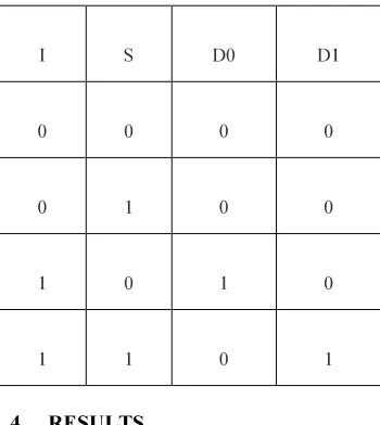
The truth table for a decoder based 1-to-2 De-multiplexer is given below in table 1, where I is the input, S is the selection line and D0, D1 are the outputs.
Table 1: Truth table of decoder based 1-to-2 Demultiplexer
4. RESULTS
The drain characteristics of the DGMOSFET are obtained using matlab software and the results obtained are represented in the Fig.4 and Fig.5 repsectively. These results are obtained by the matlab programming of the DGMOSFET model.
Figure 4: Variation of drain characteristics of DGMOSFET with Vds
Figure 5: Variation of drain characteristics of DGMOSFET with Vgs
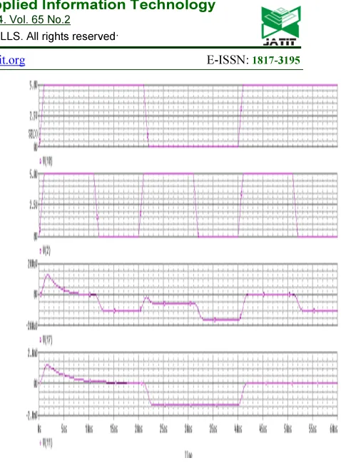
Below figures 6, 7, and 8 represents the simulation output of the DG MOSFET i.e. the input voltage at gate 1 and gate 2 of a Dual Gate MOSFET and the output is taken at the drain side, which is obtained to be 100 mv. Here x axis is taken as time in ns and y is the different voltage values in volts. These results are obtained by the SPICE Programming of the desing shown in the Figure 3 .
I S D0 D1
0 0 0 0
0 1 0 0
1 0 1 0
[image:4.595.326.492.350.562.2] [image:4.595.83.258.463.659.2][image:5.595.86.536.74.556.2]
Figure 6: Simulation output of Input voltage at gate 1 of a DG MOSFET
Figure 7: Simulation output of Input voltage at gate 2 of a DG MOSFET
[image:5.595.88.294.344.536.2]The output of a 2X1 decoder based De-multiplexer using DG MOSFET is shown below. V (10) is the input line and V (2) is the selection line. V (11) and the V (17) are the two outputs. Here x axis is the time and y axis is the voltage.
Figure 8: Simulation output for decoder based de-multiplexer
Thus the results of modeling of dual gate MOSFET were discussed and also the decoder based demultiplexer’s using dual gate MOSFET is also simulated. The modeling was carried out in MATLAB, whereas the demultiplexer was developed in PSPICE.
5. CONCLUSION AND FUTURESCOPE
development of new methodologies in the design
of combinational logic block circuits.
REFERENCES:
[ 1] Barbut L. Jazaeri F. Bouvet D. Sallese J M.( Jun.2013),” Transient off-current in junctionless FETs,”IEEE Trans. Electron Devices , vol.60, no.6, pp.2080-2083.
[ 2] Colinge J P. Kranti A.Yan R. Lee C W. Ferain I. Yu R.( Nov.2011), “ Junctionless nanowire transistor (JNT): Properties and design guidelines,” Solid –State Electron, vols.65-66,pp.33-37.
[ 3] Dixit A. Kottantharayil A. Collaert N. Goodwin M. Jurczak, and Meyar K.D. (Jun 2005), “Analysis of the parasitic S/D resistance in multiple-gate FETs,” IEEE Trans. Electron Devices, vol. 52, no. 6, pp. 1132-1140, Jun. 2005.
[ 4] Gelpey J. McCoy S. Kontos A. godet L. Hatem C. Camm D. Chan J. Papasouliote G. and Scheuer J. (May 2008), “Ultra-shallow junction formation using flash annealing and advanced doping techniques,” in Proc. 8th IJWT, pp. 82-86.
[ 5] Jazaeri F. Barbut L. and Sallese J M. (Jul.2013), “Modeling and design space of junctionless symmetric DG MOSFET with long channel,” IEEE Trans. Electron Devices, vol.60, no.7, pp.2120-2127.
[ 6] Mariniello G. Doria R. de Souza M, Pavanello M, and Trevisoli R. (Mar.2012),”Analysis of gate capacitance of n-type junctionless transistors using three dimensional device simulations,” in Proc.8th ICCDCS, pp.1-4 [ 7]Ortiz-conde A. Garcia-Sanchez F.Z. Muchi J.
Teran Barrios A. Liou J.J. and Ho C.S. (Jan 2013), “Revisiting MOSFET threshold voltage extraction methods,” Microelecton. Rel., vol. 53, no. 1, pp. 90-104.
[ 8] Omura.Y, Nakakubo.A, and Nakatsuji.H. (Nov.2011), “Quantum mechanical effect in temperature dependence of threshold voltage of extremely thin soi mosfets,” vol. 48, no. 9, pp. 1661 –1666.
[ 9] Salcedo J A. Ortiz-Conde, Garcia-Sanchez F J. Muci J, Liou J J and Yue.Y.(Apr.2001) ,”New approach for defining the threshold voltage of MOSFETs,” IEEE Trans. Electron Devices, vol. 48, no.4, pp.809-813.
[ 10] Sallese J M. Chevillon N. Lallement C. Iniguez B. Pregaldiny F.( Aug.2011) “Charge based modeling of junctionless double gate field effect transistor ,” IEEE Trans. Electron Devices, vol.58, no.8, pp.2628-2637.
[ 11] Vaddi R. Agarwal R. and Dasgupta S. (Oct 2012), “Compact modeling of a generic double gate MOSFET with gate S/D underlap,” IEEE Trans. Electron Devices, vol. 59, no. 10, pp. 2846-2849.
[ 12] MOSFET, http://en.wikipedia.org.
[ 13] Dual gate MOSFETs,
http://www.circuitstoday.com/dual-gate-mosffets.
[ 14] Demultiplexer,
![Figure 1: Cross section view of dual gate N channel type MOSFET [13]](https://thumb-us.123doks.com/thumbv2/123dok_us/8912636.960120/2.595.91.286.151.280/figure-cross-section-view-dual-gate-channel-mosfet.webp)